Page History
...
| Scroll Only (inline) |
|---|
Online version of this manual and other related documents can be found at https://wiki.trenz-electronic.de/display/PD/SC-CPLD-Firmware |
| Scroll pdf ignore | ||||
|---|---|---|---|---|
Table of contents
|
Temporary CPLD Description
| Note |
|---|
This chapter is part if an older description and can be use until the newer one is finished Please use TE0720 CPLD |
Overview: System Management Controller (SC)
A Lattice XO2-1200 CPLD is used as a System Management Controller (referred to as SC in the manual). The SC is responsible for power sequencing, reset generation and Zynq initial configuration (mode pin strapping). Moreover, some on-board ICs are connected to the SC that provides level shifting.
...
The SC wakes up when the 3.3V input power rises above 2.1V (VIN voltage is not needed). The SC can turn on or off all of the other supplies on the module (except in no power sequencing mode when the 1.0V and 1.8 V supplies are forced to start immediately when power is applied to the module).
Custom SC Programming
SC customization is available either by requesting new features or with special agreement by using the users own code. SC code can be updated in the system using the I2C interface. Please contact us for details.
SC B2B Pins
SC is connected directly to the following B2B Pins.
| Name | Mode | Default function | Alternative | Description |
|---|---|---|---|---|
| EN1 | input, weak pull-up | Power Enable | IO | High enables the DC-DC converters and on-board supplies. Not used if NOSEQ=1 |
| PGOOD | output, open drain | Power good | SCL or IO | Forced low until all on-board power supplies are working properly. Attention: During CPLD programming, this pins is high impedance |
| MODE | input, weak pull-up | Boot mode | SDA or IO | Force low for boot from the SD Card. Latched at power on only, not on soft reset! |
| RESIN | input, weak pull-up | Reset input | IO | Active Low Reset input, default mapping forces POR_B reset to Zynq PS |
| NOSEQ | input, weak pull-down | Power sequencing Control | Output | Forces the 1.0V and 1.8V DC-DC converters always ON when high. Can be used as an I/O after boot. |
| JTAGSEL | input | JTAG Chain select | none, fixed | keep GND or pulled low for FPGA JTAG access. |
NOSEQ Pin
This is a dedicated input that forces the module's 1.0V and 1.8V supplies to be enabled if high. This pin has a weak pull-down on the module. If left open the module will power up in normal power sequencing enabled mode. This pin is 3.3V tolerant. This pin is also connected to the System Management Controller. The SC can read the status of this pin (that is it can detect if the module is in power sequencing enabled mode). The SC can also use this pin as output after normal power on sequence. Please check the SC description for the function. SC rev 0.02 maps Ethernet PHY LED0 to NOSEQ by default (the mapping can be changed by software after boot).
No Sequencing mode
If the module is powered from a single 3.3V supply and power sequencing is disabled, then NOSEQ pin should be powered from the main 3.3V input. That is VIN, 3.3Vin and NOSEQ should all be tied together to the input 3.3V power rail. Sequencing mode should not be used if VIN is not 3.3V.
Normal mode
For normal operation leave NOSEQ open or pull down with a resistor.
Normal mode with user function on NOSEQ
NOSEQ can be used as an output after boot. NOSEQ must be low when 3.3V power is applied to the module. Common usage is an LED connected between NOSEQ and GND.
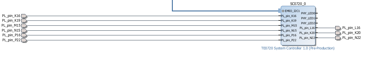
SC pins to the FPGA
| Schematic net name | Default function | Direction | SC pin | FPGA pin | Description | |||
|---|---|---|---|---|---|---|---|---|
| XCLK | ETH PHY Clock to FPGA | to FPGA | K1 | K19 | ||||
| X1 | I2C Clock from FPGA | from FPGA | F1 | L16 | SCL from EMIO I2Cx | |||
| X7 | I2C Data from FPGA | from FPGA | M1 | N22 | SDA from EMIO I2Cx | |||
| X5 | I2C Data to FPGA | to FPGA | J1 | P22 | SDA to EMIO I2Cx | |||
| X2 | ETH PHY LED1LED0 | to FPGA | C2 | M15 | ||||
| X4 | ETH PHY LED2 | to FPGA | D1 | P16 | ||||
| X3Interrupt | ETH PHY LED1 | to FPGA | B1 | N15 | RTC, MEMS Interrupt or PHY LED3LED1 | |||
| X0 | - | - | not used on TE0720-02 | |||||
| PUDC | K16 | normally not used tied to fixed level by SC |
...
It is recommended to use Vivado IP Core available for 2014.2 and later versions.
Default Mode
At power up the System Management Controller starts with default settings.
| Pin/Function | Used as/Mapped to | Notes | ||
|---|---|---|---|---|
| ETH PHY LED0 | XIO to FPGA | |||
| ETH PHY LED1 | XIO to FPGA | |||
| ETH PHY LED2 | Not used | XIO to FPGA | ||
| ETH PHY CONFIG | Tied logic low | PHY Address set to 0 | ||
| ETH CLK125MHz | Pass through FPGA B34 SRCC pin | |||
| ETH Clock Enable | Tied logic high | |||
| ETH PHY Reset | Internal RESET | |||
| MIO7 | LED1 | |||
| MEMS/RTC I2C | XIO to FPGA | |||
| RTC Interrupt | - | |||
| MEMS Interrupt 1 | - | |||
| MEMS Interrupt 2 | - | |||
| eMMC Reset | Internal RESET | |||
| USB PHY Reset | Internal RESET | |||
| FPGA FPGA PUDC | Tied logic low | |||
| FPGA PROG_B | Tied logic high | |||
| Zynq Cascaded JTAG | Enabled (pulled low) | |||
| Zynq boot mode | SPI or SD, depending on bootmode pin | |||
| Zynq SRST | Tied logic high | |||
| Zynq POR | Internal POR/Reset | |||
| PLL | Not used | |||
| LED2 | System Status LED | |||
| LED1 | MIO7 | |||
| NOSEQ Input | NOSEQ at power, LED out after boot | |||
| Power Good 1.5V | ||||
| Power Good VTT | ||||
| MODE Input |
| I2C Address | Function | |
|---|---|---|
| 0x20 | Status reg 1 | |
| 0x21 | Status reg 2 |
LED Control Status
The TE0720 on-board LED devices can be remapped to different functions.
...
| D3 | D2 | D1 | D0 | LED1 function as |
|---|---|---|---|---|
| 0 | 0 | 0 | 0 | Default (MIO7) |
| 0 | 0 | 0 | 1 | ETH PHY LED0 |
| 0 | 0 | 1 | 0 | ETH PHY LED1 |
| 0 | 0 | 1 | 1 | ETH PHY LED2 |
| 0 | 1 | 0 | 0 | MIO7 |
| 0 | 1 | 0 | 1 | Undefined |
| 0 | 1 | 1 | 0 | OFF |
| 0 | 1 | 1 | 1 | ON |
| 1 | x | x | x | Undefined |
SC Demystified
System Controller (SC for short) was designed to allow ZYNQ PS system to access module special functions as early as possible without reducing the number of MIO pins that are fully user configurable.
...
For most use cases the only need to use this interface is access to MAC Address info, this is normally done by u-boot loader that fetches the MAC Address bytes and sets its environment variables accordingly. Linux image will then also be started so that the MAC Address from EEPROM is used for Ethernet 0 Physical interface.
SC Firmware ver 0.02
This is the initial version of the System Controller with only a very limited function set implemented.
...
zynq-uboot> printenv board
board=TE0720-01-2IF
zynq-uboot>
Reading MAC Address
With u-boot command mii read:
...
Customized u-boot does read MAC Address and stores it in environment variables as required, as a result, proper MAC address is used both in u-boot as also in Linux. Setting up MAC Address for Linux involves dynamic rewrite of FDT, this is done with u-boot script that starts Linux.
SC Registers
Most registers and functions are available via ETH PHY Management interface (MIO pins 52 and 53).
| Addr | R/W | Register name | Descripion | ||
|---|---|---|---|---|---|
| 0 | RO | ||||
| 1 | RO | ||||
| 2 | RO | ID1 | Identifier Register 1 | ||
| 3 | RO | ID2 | Identifier Register 2 | ||
| 4 | RO | ID3 | Identifier Register 3 | ||
| 5 | RW | CR1 | Control Register 1: LED's | ||
| 6 | RW | CR2 | Control Register 2; XIO Control | ||
| 7 | RW | CR3 | Control Register 3; Reset, Interrupt | ||
| 8 | RO | SR1 | Status Register | ||
| 9 | RO | MAChi | Highest bytes of primary MAC Address | ||
| 0xA | RO | MACmi | Middle bytes of primary MAC Address | ||
| 0xB | RO | MAClo | Lowest bytes of primary MAC Address | ||
| 0xC | CR4 | reserved do not use | |||
| 0xD | RW | MMD_CR | MMD Control Register | ||
| 0xE | RW | MMD_AD | MMD Address/Data | ||
| 0xF | - | reserved do no use | |||
| other | - | reserved do not use |
Register CR1
| Bit | Description |
|---|---|
| 15:12 | - |
| 11:8 | Noseq MUX |
| 7:4 | LED2 MUX |
| 3:0 | LED1 MUX |
| Value | LED1 | LED2 | NOSEQ | ||||
|---|---|---|---|---|---|---|---|
| Default | MIO7 | Mode Blink | PHY_LED0 | ||||
| 0001 | PHY_LED0 | PHY_LED0 | PHY_LED0 | ||||
| 0010 | PHY_LED1 | PHY_LED1 | PHY_LED1 | ||||
| 0011 | PHY_LED2 | PHY_LED2 | PHY_LED2 | ||||
| 0100 | MIO7 | MIO7 | MIO7 | ||||
| 0101 | RTC_INT | RTC_INT | RTC_INT | ||||
| 0110 | OFF | OFF | OFF | ||||
| 0111 | ON | ON | ON | ||||
| 1000 | MIO14/MIO15 | MIO14/MIO15 | REV 05, UART activity | ||||
| 1001 | MIO14 | MIO15 | REV 05 | ||||
| 1010 | REV 05 |
...
Register CR2
| Bit | Description |
|---|---|
| 15:12 | XCLK select |
| 11:8 | XIO6 select |
| 7:4 | XIO5 select |
| 3:0 | XIO4 select |
...
Signal XIO4
| XIO4 select | Signal out value |
|---|---|
| "0001" | MIO7 |
| "0010" | SHA_IO |
| "0011" | MAC_IO |
| "0110" | 'Z' (Configured as input) |
| all others | PHY_LED0 |
...
Signal XIO5
| XIO5 select | Signal out value |
|---|---|
| "0101" | RTC_INT |
| "0110" | 'Z' (Configured as input) |
| all others | PHY_LED1 |
...
Signal XIO6
| XIO6 select | Signal out value |
|---|---|
| "0110" | 'Z' (Configured as input) |
| "0111" | INTR |
| all others | PHY_LED2 |
Signal XCLK
| XCLK Select | Signal out value |
|---|---|
| "0001" | RTC_INT |
| "0010" | Internal Oscillator Out ~24.18 MHz |
| all others | 125 MHz |
...
Signal SHA_IO
| XIO4 select | Signal out value |
|---|---|
| "0010" | XIO5 |
| all others | 'Z' (Configured as input) |
...
Signal MAC_IO
| XIO4 Select | Signal out value |
|---|---|
| "0011" | XIO5 |
| all others | Connected to internal MAC read block |
...
System Controller version 0.02 does not support extended address space - registers 0xD and 0xE are read-write accessible but do not have any function. In feature revision extended address will be used to control SC PLL and other features.
| Bit | Description |
|---|---|
| 0 | enable INT1 |
| 1 | enable INT2 |
| 2 | enable RTC_INT |
| 3 | enable PHY_LED2 |
CR3 bit description
| 4 | OTG_RST |
| 5 | ETH_RST |
| 6 | MMC_RST |
| 7 | EN_ETH_CLK (not CR3, default enabled) |
CR3 bit description
Interrupt can be selected instead of PHY_LED2 on XIO6 pin, Interrupt can be selected instead of PHY_LED2 on XIO6 pin, by setting CR2 bits 11 downto 8 to "0111"
Overview: On-board LEDs
There are 3 on-board LEDs, with two of them connected to the System Management Controller and one to the Zynq PL (Done pin).
| Name | Color | Connected to: | Default mapping: |
|---|---|---|---|
| LED1 | Green | SC | PL MIO[7] |
| LED2 | Red | SC | System Controller Status LED |
| LED3 | Green | Zynq PL | FPGA Done - active low |
LED1 GREEN
Is mapped to MIO7 after power up. After the Zynq PS has booted it can change the mapping of this LED. If SC can not enable power to the Zynq then this LED will remain under SC control. It is available to the user only after the power supplies have stabilized and the POR reset to the Zynq is released.
LED2 RED
Is used by the SC as global status LED. The SC can show status information on this LED. Vin power is not required.
LED3 GREEN (FPGA Done)
This green LED is connected to the FPGA Done pin which has an active low state. As soon as the Zynq is powered and the 3.3V I/O voltage is enabled, this LED will illuminate. This indicates that the Zynq PL is not configured. Once the Zynq PL has been configured the LED will go off.
During normal operation when the Zynq PL has been configured, the LED can be controlled from the FPGA fabric. Control of the LED in a user design requires the use of Xilinx startup primitive rather than a normal I/O primitive. If the startup primitive is not used then the LED will go off after configuration and remain off irrespectively of the user design. This LED can not be controlled by the SC.
| Note |
|---|
| This LED will not operate if the SC can not power on the 3.3V output rail that also powers the 3.3V circuitry on the module. |
LED Status Codes
| # | GLED1 | RLED2 | GLED3 | Status | Description |
|---|---|---|---|---|---|
| 1 | OFF | OFF | ON | Fatal power error | This combination after power up is only possible in no sequencing compatibility mode were 3.3Vout is supplied externally. The 1.0V and 1.8V DC-DC supplies are forced on (NOSEQ=1), and the SC is not able to start (3.3Vin below 2.1V). This should never happen if the external power supplies are OK. |
| 2 | OFF | ON | OFF | VIN missing (or EN1 low) | 3.3Vin is present, but the DC-DC supplies are not powered or 3.3Vin is below 3.05V. If the LEDs stay on in this state then 3.3Vout is not turned on, and the Zynq is kept in the POR state. |
| 3 | OFF | 1/2 Blink Fast 4 Hz | ON | OK | Boot mode selected is SPI Flash. This status remains after boot also if the LED settings are not changed and user is not controlling MIO7 and FPGA is not loaded. |
| 4 | OFF | 1/2 Blink Slow 1 Hz | ON | OK | Boot mode selected is SD Card. This status remains after boot also if the LED settings are not changed and user is not controlling MIO7 and FPGA is not loaded. |
| 5 | MIO7 or user function | Blink or user function | OFF | OK | LED3 goes off when the FPGA is configured. NOTE: The FPGA design can control this LED too using STARTUPE2, so it may remain ON or be flashing when the FPGA is configured. |
| 6 | ON | Slow blink 0.5Hz, 1/8 on, 7/8 off | OFF | Powerdown | EN1 input to the module is low. If sequencing is enabled in this mode, then all power supplies on the module are OFF. |
| 7 | ON | Slow blink 0.5Hz, 1/8 on, 7/8 off | ON | EN1 input to the module is low. Sequencing is disabled module is in reset state. | |
| 8 | ON | ON | ON | Reset | Powered, RESIN input is active low or Bank B34 Supply Voltage is missing. |
If green LED3 does not light up at least for short time at power then there is major problem with power supplies, FPGA core and aux voltages may be missing.
| HTML |
|---|
<!-- |
Overview
Firmware for PCB CPLD with designator U19. CPLD Device in Chain: LCMX02-1200HC
Feature Summary
Firmware Revision and supported PCB Revision
See Document Change History
Product Specification
Port Description
| Name / opt. VHD Name | Direction | Pin | Bank Power | Description |
|---|---|---|---|---|
Functional Description
| HTML |
|---|
--> |
Appx. A: Change History and Legal Notices
Revision Changes
Document Change History
To get content of older revision got to "Change History" of this page and select older document revision number.
...
| Date | Document Revision | CPLD Firmware Revision | Supported PCB Revision | Authors | Description | ||||||||||||||||||||||
|---|---|---|---|---|---|---|---|---|---|---|---|---|---|---|---|---|---|---|---|---|---|---|---|---|---|---|---|
|
| --- | --- |
| Work in progress | ||||||||||||||||||||||
| 2019-03-25 | v.1 | --- | --- |
| Initial release | ||||||||||||||||||||||
| All |
|
Legal Notices
| Include Page | ||||
|---|---|---|---|---|
|
...
Overview
Content Tools