...
| Page properties |
|---|
|
- Overview of Boot Mode, Reset, Enables.
|
The FPGA configuration for Intel MAX 10 FPGAs can be stored through JTAG interface either in external configuration device (QSPI flash memory U5) or on the FPGA itself since the Intel MAX 10 FPGA offers non-volatile memory on chip. The FPGA configuration is loaded from the non-volatile memory when the board is powered up.
To configure the FPGA directly, the JTAG interface can be used to configure the FPGA volatile, means the configuration is lost after power off.
Reset process must be done by pressing push button S1.
| Scroll Title |
|---|
| anchor | Table_OV_RST |
|---|
| title | Reset process. |
|---|
|
| Scroll Table Layout |
|---|
| orientation | portrait |
|---|
| sortDirection | ASC |
|---|
| repeatTableHeaders | default |
|---|
| style | |
|---|
| widths | |
|---|
| sortByColumn | 1 |
|---|
| sortEnabled | false |
|---|
| cellHighlighting | true |
|---|
|
Signal | Push Button | Pin Header | Note |
|---|
RESET | S1 | J2 | connected to nCONFIG |
|
Signals, Interfaces and Pins
| Page properties |
|---|
|
Notes : - For carrier or stand-alone boards use subsection for every connector type (add designator on description, not on the subsection title), for example:
- For modules which needs carrier use only classes and refer to B2B connector if more than one is used, for example
|
I/Os on Pin Headers and Connectors
| Scroll Title |
|---|
| anchor | Table_SIP_GIOs |
|---|
| title | General I/Os to Pin Headers and connectors information |
|---|
|
| Scroll Table Layout |
|---|
| orientation | portrait |
|---|
| sortDirection | ASC |
|---|
| repeatTableHeaders | default |
|---|
| style | |
|---|
| widths | |
|---|
| sortByColumn | 1 |
|---|
| sortEnabled | false |
|---|
| cellHighlighting | true |
|---|
|
| FPGA Bank | Connector Designator | I/O Signal Count | Voltage Level | Notes |
|---|
| Bank 1A | J1 | 7 | 3.3V | AIN0...6 | | Bank 1B | J4 | 5 | 3.3V | JTAG interface | | Bank 2 | J1 | 4 | 3.3V | DIO2...5 | | Bank 5 | J2 | 9 | 3.3V | DIO6...14 | | J1 | 2 | 3.3V | DIO0...1 | | Bank 8 | J2 | 1 | 3.3V | RESET |
|
FPGA I/O Banks
| Page properties |
|---|
|
you must fill the table below with group of MIOs which are connected to a specific components or peripherals, you do not have to specify pins in B2B, Just mention which B2B is connected to MIOs. The rest is clear in the Schematic. Example: | MIO Pin | Connected to | B2B | Notes |
|---|
| MIO12...14 | SPI_CS , SPI_DQ0... SPI_DQ3 SPI_SCK | J2 | QSPI |
|
| Scroll Title |
|---|
| anchor | Table_OV_BP |
|---|
| title | Boot process. |
|---|
|
| Scroll Table Layout |
|---|
|
| orientation | portrait |
|---|
| sortDirection | ASC |
|---|
| repeatTableHeaders | default |
|---|
style | widths | | sortByColumn | 1 |
|---|
| sortEnabled | false |
|---|
| cellHighlighting | true |
|---|
MODE Signal State | Boot Mode
| Scroll Title |
|---|
| anchor | Table_OVOBP_RSTIOs |
|---|
| title | Reset process.FPGA I/O Banks |
|---|
|
| Scroll Table Layout |
|---|
| orientation | portrait |
|---|
| sortDirection | ASC |
|---|
| repeatTableHeaders | default |
|---|
| style | |
|---|
| widths | |
|---|
| sortByColumn | 1 |
|---|
| sortEnabled | false |
|---|
| cellHighlighting | true |
|---|
|
|
Signal | B2B | I/O | Note |
|---|
Signals, Interfaces and Pins
| Page properties |
|---|
|
Notes : - For carrier or stand-alone boards use subsection for every connector type (add designator on description, not on the subsection title), for example:
- For modules which needs carrier use only classes and refer to B2B connector if more than one is used, for example
|
Board to Board (B2B) I/Os
FPGA bank number and number of I/O signals connected to the B2B connector:
...
| anchor | Table_SIP_B2B |
|---|
| title | General PL I/O to B2B connectors information |
|---|
...
| FPGA Bank | I/O Signal Count | Connected to | Notes |
|---|
| Bank 1A | 7 | 1x14 Pin header, J1 | AIN0...6 | | 1 | Jumper, J3 | AIN7 | | Bank 1B | 5 | 1x6 Pin header, J4 | JTAG_EN, TDI, TDO, TMS, TCK | Bank 2
| 4 | 1x14 Pin header, J1 | D2...5 | | 5 | A2D, U15 | ADC_EN, ADC_SDI, ADC_SDO, ADC_SCK, ADC_CNV | | 1 | 12MHz Oscillator, U7 | CLK12M | | 2 | Amplifier, U12 | nIAMP_A0, nIAMP_A1 | | Bank 3 | 22 | SDRAM, U2 | RAM_ADDR_CMD | | Bank 5 | 9 | 1x14 Pin header, J2 | DIO6...14 | | 2 | 1x14 Pin header, J1 | DIO0...1 | | 1 | D12_R | DIO12 | | Bank 6 | 16 | SDRAM, U2 | DQ0...15 | | 2 | SDRAM, U2 | DQM0...1 | | 1 | D11_R | DIO11 | Bank 8
| 8 | User Red LEDs, D2...9 | LED0...7 | | 6 | SPI Flash, U5 | F_CS, F_CK, F_DI, F_DO, nSTATUS, DEVCLRn | | 1 | Red LED, D10 | CONF_DONE | | 6 | FTDI JTAG/UART Adapter, U3 | BDBUS0...5 | | 1 | Push Button, S2 | USER_BTN |
|
JTAG Interface
JTAG access to the TExxxx TEI0015 SoM through B2B pin header connector JMXJ4.
| Scroll Title |
|---|
| anchor | Table_SIP_JTG |
|---|
| title | JTAG pins connection |
|---|
|
| Scroll Table Layout |
|---|
| orientation | portrait |
|---|
| sortDirection | ASC |
|---|
| repeatTableHeaders | default |
|---|
| style | |
|---|
| widths | |
|---|
| sortByColumn | 1 |
|---|
| sortEnabled | false |
|---|
| cellHighlighting | true |
|---|
|
B2B Pin Header Connector | Note |
|---|
| TMS | J4-6 |
| | TDI |
TDO| J4-5 |
| | TDO | J4-4 |
| | TCK | J4-3 |
| | JTAG_EN |
|
...
On-board Peripherals
| Page properties |
|---|
| you must fill the table below with group of MIOs which are connected to a specific components or peripherals, you do not have to specify pins in B2B, Just mention which B2B is connected to MIOs. The rest is clear in the Schematic.
Example:
| MIO Pin | Connected to | B2B | Notes |
|---|
| MIO12...14 | SPI_CS , SPI_DQ0... SPI_DQ3 SPI_SCK | J2 | QSPI |
Notes : - add subsection for every component which is important for design, for example:
- Two 100 Mbit Ethernet Transciever PHY
- USB PHY
- Programmable Clock Generator
- Oscillators
- eMMCs
- RTC
- FTDI
- ...
- DIP-Switches
- Buttons
- LEDs
|
| Page properties |
|---|
|
Notes : In the on-board peripheral table "chip/Interface" must be linked to the corresponding chapter or subsection |
| Scroll Title |
|---|
| anchor | Table_OBP_MIOs |
|---|
| title | MIOs pinsOn board peripherals |
|---|
|
| Scroll Table Layout |
|---|
| orientation | portrait |
|---|
| sortDirection | ASC |
|---|
| repeatTableHeaders | default |
|---|
| style | widths |
|---|
| sortByColumn | 1 |
|---|
| sortEnabled | false |
|---|
| cellHighlighting | true |
|---|
|
|
| MIO Pin | Connected to | B2B | Notes |
|---|
...
| |
|---|
| widths | |
|---|
| sortByColumn | 1 |
|---|
| sortEnabled | false |
|---|
| cellHighlighting | true |
|---|
|
|
SDRAM
TEI0015 is equipped with a Winbond 64 MBit (8 MByte) SDRAM chip in standard configuration, variants with 256 Mbit (32 MByte) memory density are also available. The SDRAM chip is connected to the FPGA bank 3 and 6 via 16-bit memory interface with 166MHz clock frequency and CL3 CAS latency.
| Page properties |
|---|
|
Notes : - add subsection for every component which is important for design, for example:
- Two 100 Mbit Ethernet Transciever PHY
- USB PHY
- Programmable Clock Generator
- Oscillators
- eMMCs
- RTC
- FTDI
- ...
- DIP-Switches
- Buttons
- LEDs
|
| Page properties |
|---|
|
Notes : In the on-board peripheral table "chip/Interface" must be linked to the corresponding chapter or subsection |
...
| anchor | Table_OBP |
|---|
| title | On board peripherals |
|---|
...
Quad SPI Flash Memory
...
Notes :
...
Minimum and Maximum density of quad SPI flash must be mentioned for other assembly options. |
| Scroll Title |
|---|
| anchor | Table_OBP_SDRAM |
|---|
| title | SDRAM interface IOs and pins |
|---|
|
| Scroll Table Layout |
|---|
| orientation | portrait |
|---|
| sortDirection | ASC |
|---|
| repeatTableHeaders | default |
|---|
| style | |
|---|
| widths | |
|---|
| sortByColumn | 1 |
|---|
| sortEnabled | false |
|---|
| cellHighlighting | true |
|---|
|
| SDRAM I/O Signals | Signal Schematic Name | Connected to | Notes |
|---|
| Address inputs | A0 ... A13 | bank 3 | - | Bank address inputs
| BA0 / BA1 | bank 3 | - | | Data input/output | DQ0 ... DQ15 | bank 6 | - | | Data mask | DQM0 ... DQM1 | bank 6 | - | | Clock | CLK | bank 3 |
| | Control Signals | CS | bank 3 | Chip select | CKE | bank 3 | Clock enable | RAS | bank 3 | Row Address Strobe | CAS | bank 3 | Column Address Strobe | | WE | bank 3 | Write Enable |
|
FTDI FT2232H
The FTDI chip U3 converts signals from USB2 to a variety of standard serial and parallel interfaces. Refer to the FTDI data sheet to get information about the capacity of the FT2232H chip.
FTDI FT2232H chip is used in MPPSE mode for JTAG, 6 I/O's of Channel B are routed to FPGA bank 8 of the FPGA SoC and are usable for example as GPIOs, UART or other standard interfaces.
The configuration of FTDI FT2232H chip is pre-programmed on the EEPROM U9.
| Scroll Title |
|---|
| anchor | Table_OBP_SPIFTDI |
|---|
| title | Quad SPI interface MIOs FTDI chip interfaces and pins |
|---|
|
| Scroll Table Layout |
|---|
| orientation | portrait |
|---|
| sortDirection | ASC |
|---|
| repeatTableHeaders | default |
|---|
| style | |
|---|
| widths | |
|---|
| sortByColumn | 1 |
|---|
| sortEnabled | false |
|---|
| cellHighlighting | true |
|---|
|
MIO | FTDI Chip U3 Pin | Signal Schematic |
|---|
U?? Pin |
...
| anchor | Table_OBP_RTC |
|---|
| title | I2C interface MIOs and pins |
|---|
|
|---|
| ADBUS0 | TCK | FPGA bank 1B, pin G2 | JTAG interface | | ADBUS1 | TDI | FPGA bank 1B, pin F5 | | ADBUS2 | TDO | FPGA bank 1B, pin F6 | | ADBUS3 | TMS | FPGA bank 1B, pin G1 | | BDBUS0 | BDBUS0 | FPGA bank 8, pin A4 | user configurable | | BDBUS1 | BDBUS1 | FPGA bank 8, pin B4 | user configurable | | BDBUS2 | BDBUS2 | FPGA bank 8, pin B5 | user configurable | | BDBUS3 | BDBUS3 | FPGA bank 8, pin A6 | user configurable | | BDBUS4 | BDBUS4 | FPGA bank 8, pin B6 | user configurable | | BDBUS5 | BDBUS5 | FPGA bank 8, pin A7 | user configurable |
|
SPI Flash Memory
On-board serial configuration memory (U5) is provided by Winbond with 64 MBit (8 MByte) storage capacity. This non volatile memory is used to store initial FPGA configuration via JTAG interface. The memory is connected to FPGA bank 8 via SPI interface.
...
| Scroll Title |
|---|
| anchor | Table_OBP_I2C_RTCQSPI |
|---|
| title | I2C Address for RTCQuad SPI Flash memory interface |
|---|
|
| Scroll Table Layout |
|---|
| orientation | portrait |
|---|
| sortDirection | ASC |
|---|
| repeatTableHeaders | default |
|---|
| style | |
|---|
| widths | |
|---|
| sortByColumn | 1 |
|---|
| sortEnabled | false |
|---|
| cellHighlighting | true |
|---|
|
|
| MIO Pin | I2C Address | Designator | Notes |
|---|
...
| anchor | Table_OBP_EEP |
|---|
| title | I2C EEPROM interface MIOs and pins |
|---|
| Signal Schematic Name | Connected to | Notes |
|---|
| F_CS | FPGA bank 8, pin B3 | chip select | | F_CLK | FPGA bank 8, pin A3 | clock | | F_DI | FPGA bank 8, pin A2 | data in / out | | nSTATUS | FPGA bank 8, pin C4 | data in / out, configuration dual-purpose pin of FPGA | | DEVCLRN | FPGA bank 8, pin B9 | data in / out, configuration dual-purpose pin of FPGA | | F_DO | FPGA bank 8, pin B2 | data in / out |
|
EEPROM
The configuration of FTDI FT2232H chip is pre-programmed on the EEPROM U9.
...
| Scroll Title |
|---|
| anchor | Table_OBP_I2C_EEPROMEEP |
|---|
| title | I2C address for EEPROM interface MIOs and pins |
|---|
|
| Scroll Table Layout |
|---|
| orientation | portrait |
|---|
| sortDirection | ASC |
|---|
| repeatTableHeaders | default |
|---|
| style | |
|---|
| widths | |
|---|
| sortByColumn | 1 |
|---|
| sortEnabled | false |
|---|
| cellHighlighting | true |
|---|
|
|
| MIO Pin | I2C Address | Designator | Notes |
|---|
LEDs
| Schematic | Connected to | Notes |
|---|
EECS | FTDI U3, Pin EECS |
| | EECLK | FTDI U3, Pin EECLK |
| | EEDATA | FTDI U3, Pin EEDATA |
|
|
A2D Convertor
The TEI0010 board is equipped with the Analog Devices AD4003BCPZ, 18-bit A2D converter (ADC).
| Scroll Title |
|---|
| anchor | Table_OBP_LEDA2D |
|---|
| title | On-board LEDsA2D converter interface and pins |
|---|
|
| Scroll Table Layout |
|---|
| orientation | portrait |
|---|
| sortDirection | ASC |
|---|
| repeatTableHeaders | default |
|---|
| style | |
|---|
| widths | |
|---|
| sortByColumn | 1 |
|---|
| sortEnabled | false |
|---|
| cellHighlighting | true |
|---|
|
Schematic| Color | Active LevelNote | |
DDR3 SDRAM
| Page properties |
|---|
|
Notes : Minimum and Maximum density of DDR3 SDRAM must be mentioned for other assembly options. (pay attention to supported address length for DDR3) |
The TE???? SoM has ??? GByte volatile DDR3 SDRAM IC for storing user application code and data.
- Part number:
- Supply voltage:
- Speed:
- NOR Flash
- Temperature:
...
IN+ | Diff Amplifier U14, VOUT- |
| | IN- | Diff Amplifier U14, VOUT+ |
| | SDI | Bank 2, ADC_SDI |
| | SDO | Bank 2, ADC_SDO |
| | SCK | Bank 2, ADC_SCK |
| | CNV | Bank 2, ADC_CNV |
|
|
LEDs
| Scroll Title |
|---|
| anchor | Table_OBP_ETHLED |
|---|
| title | Ethernet PHY to Zynq SoC connectionsOn-board LEDs |
|---|
|
| Scroll Table Layout |
|---|
| orientation | portrait |
|---|
| sortDirection | ASC |
|---|
| repeatTableHeaders | default |
|---|
| style | |
|---|
| widths | |
|---|
| sortByColumn | 1 |
|---|
| sortEnabled | false |
|---|
| cellHighlighting | true |
|---|
|
|
| Bank | Signal Name | ETH1 | ETH2 | Signal Description |
|---|
...
| Designator | Color | Connected to | Active Level | Note |
|---|
| D2...9 | Red | LED1...8 | Active High | User LEDs | | D10 | Red | CONF_DONE | Active Low | Configuration DONE LED | | D1 | Green | 3.3V Power Rail | Active High | After power on it will be on |
|
Micro-USB2 Connector
The Micro-USB2 connector J9 provides an interface to access the UART and JTAG functions via FTDI FT2232 chip. The use of this feature requires that USB driver is installed on your host PC.
| Scroll Title |
|---|
| anchor | Table_OBP_CANUSB |
|---|
| title | CAN Tranciever interface MIOsMicro USB-2 connector pins |
|---|
|
| Scroll Table Layout |
|---|
| orientation | portrait |
|---|
| sortDirection | ASC |
|---|
| repeatTableHeaders | default |
|---|
| style | |
|---|
| widths | |
|---|
| sortByColumn | 1 |
|---|
| sortEnabled | false |
|---|
| cellHighlighting | true |
|---|
|
Bank| Schematic | U?? Pin | Notes | D-Tx | Driver Input | R-Rx | Reciever Output| VBUS | USB_VBUS | It is connected to GND | | D+ | FTDI U3, DP pin |
| | D- | FTDI U3, DM pin |
|
|
Clock Sources
| Scroll Title |
|---|
| anchor | Table_OBP_CLK |
|---|
| title | Osillators |
|---|
|
| Scroll Table Layout |
|---|
| orientation | portrait |
|---|
| sortDirection | ASC |
|---|
| repeatTableHeaders | default |
|---|
| style | |
|---|
| widths | |
|---|
| sortByColumn | 1 |
|---|
| sortEnabled | false |
|---|
| cellHighlighting | true |
|---|
|
| DesignatorClock Source | DescriptionSchematic Name | Frequency | Note | MHz | MHz | KHz |
|---|
| Microchip MEMS Oscillator, U7 | CLK12M | 12.00 MHz | Connected to FTDI FT2232 U3, pin 3 Connected to FPGA SoC bank 2, pin H6 |
|
Power and Power-On Sequence
| Page properties |
|---|
|
In 'Power and Power-on Sequence' section there are three important digrams which must be drawn: - Power on-sequence
- Power distribution
- Voltage monitoring circuit
|
Power Supply
Power To power-up the module, power supply with minimum current capability of xx A for system startup 1A is recommended.
Power Consumption
| Scroll Title |
|---|
| anchor | Table_PWR_PC |
|---|
| title | Power Consumption |
|---|
|
| Scroll Table Layout |
|---|
| orientation | portrait |
|---|
| sortDirection | ASC |
|---|
| repeatTableHeaders | default |
|---|
| style | |
|---|
| widths | |
|---|
| sortByColumn | 1 |
|---|
| sortEnabled | false |
|---|
| cellHighlighting | true |
|---|
|
| Power Input Pin | Typical Current |
|---|
| VIN | TBD* |
|
* TBD - To Be Determined
Power Distribution Dependencies
* TBD - To Be Determined
Power Distribution Dependencies
| Scroll Title |
|---|
| anchor | Figure_PWR_PD |
|---|
| title | Power Distribution |
|---|
|
| Scroll Ignore |
|---|
| draw.io Diagram |
|---|
| border | false |
|---|
| viewerToolbar | true |
|---|
| |
|---|
| fitWindow | false |
|---|
| diagramDisplayName | |
|---|
| lbox | true |
|---|
| revision | 3 |
|---|
| diagramName | TEI0015 |
|---|
|
|
|
| Scroll Title |
|---|
| anchor | Figure |
|---|
| title | Power Distribution |
|---|
| simpleViewer | false |
|---|
| width | |
|---|
| links | auto |
|---|
| tbstyle | hidden |
|---|
| diagramWidth | 641 |
|---|
|
|
| Scroll Only |
|---|
 Image Added Image Added
|
| Scroll Ignore |
|---|
Create DrawIO object here: Attention if you copy from other page, objects are only linked. |
| Scroll Only |
|---|
image link to the generate DrawIO PNG file of this page. This is a workaround until scroll pdf export bug is fixed |
|
Power-On Sequence
| Scroll Title |
|---|
| anchor | Figure_PWR_PS |
|---|
| title | Power Sequency |
|---|
|
| Scroll Ignore |
|---|
| draw.io Diagram |
|---|
| border | false |
|---|
| viewerToolbar | true |
|---|
| |
|---|
| fitWindow | false |
|---|
| diagramDisplayName | |
|---|
| lbox | true |
|---|
| revision | 3 |
|---|
| diagramName | TEI0015_PWR_PS |
|---|
| simpleViewer | false |
|---|
| width | |
|---|
| links | auto |
|---|
| tbstyle | hidden |
|---|
| diagramWidth | 641 |
|---|
|
|
| Scroll Only |
|---|
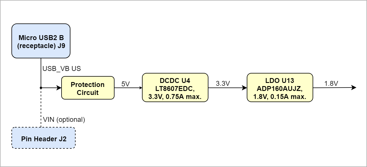 Image Added Image Added
| Create DrawIO object here: Attention if you copy from other page, objects are only linked. | | Scroll Only |
|---|
image link to the generate DrawIO PNG file of this page. This is a workaround until scroll pdf export bug is fixed |
|
Voltage Monitor Circuit
| Scroll Title |
|---|
| anchor | Figure_PWR_VMC |
|---|
| title | Voltage Monitor Circuit |
|---|
|
| Scroll Ignore |
|---|
Create DrawIO object here: Attention if you copy from other page, objects are only linked. |
| Scroll Only |
|---|
image link to the generate DrawIO PNG file of this page. This is a workaround until scroll pdf export bug is fixed |
|
...
| Scroll Title |
|---|
| anchor | Table_PWR_PR |
|---|
| title | Module power rails. |
|---|
|
| Scroll Table Layout |
|---|
| orientation | portrait |
|---|
| sortDirection | ASC |
|---|
| repeatTableHeaders | default |
|---|
| style | |
|---|
| widths | |
|---|
| sortByColumn | 1 |
|---|
| sortEnabled | false |
|---|
| cellHighlighting | true |
|---|
|
| Connector Designator | VCC / VCCIO Schematic Name | Voltage | Direction | Notes |
|---|
J2
| VIN | 5V | Input |
| | 3.3V | 3.3V | Output |
| | 5V | 5V | Output |
| J9 | USB_VBUS | 5V | Input |
Power Rail Name | B2B Connector JM1 Pin | B2B Connector JM2 Pin | B2B Connector JM3 Pin | Direction | Notes
|
Bank Voltages
| Scroll Title |
|---|
| anchor | Table_PWR_BV |
|---|
| title | Zynq SoC bank voltages. |
|---|
|
| Scroll Table Layout |
|---|
| orientation | portrait |
|---|
| sortDirection | ASC |
|---|
| repeatTableHeaders | default |
|---|
| style | |
|---|
| widths | |
|---|
| sortByColumn | 1 |
|---|
| sortEnabled | false |
|---|
| cellHighlighting | true |
|---|
|
| Notes |
|---|
| Bank 1A | VCCIO1A | 3.3V |
| | Bank 1B | VCCIO1B | 3.3V |
| | Bank 2 | VCCIO2 | 3.3V |
| | Bank 3 | VCCIO3 | 3.3V |
| | Bank 5 | VCCIO5 | 3.3V |
| | Bank 6 | VCCIO6 | 3.3V |
| | Bank 8 | VCCIO8 | 3.3V |
Notes
|
Board to Board Connectors
...
| Scroll Title |
|---|
| anchor | Table_TS_AMR |
|---|
| title | PS absolute maximum ratings |
|---|
|
| Scroll Table Layout |
|---|
| orientation | portrait |
|---|
| sortDirection | ASC |
|---|
| repeatTableHeaders | default |
|---|
| style | |
|---|
| widths | |
|---|
| sortByColumn | 1 |
|---|
| sortEnabled | false |
|---|
| cellHighlighting | true |
|---|
|
| Description | Min | Max | Unit | | Min | Max | Unit | Reference Document |
|---|
VIN supply voltage (5.0V nominal) | 4.75 | 5.25 | V |
| | I/O Input voltage for FPGA I/O bank | -0.5 | 4.12 | V | Intel MAX 10 datasheet | | Voltage on ADC IC U15 pins | -5.0 | 5.0 | V | AD4003BCPZ datasheet | | Analog reference voltage on IC U15 | 5.0 | 5.0 | V | AD4003BCPZ datasheet | Storage Temperature | -40 | +85 | °C |
V | V | V | V | V | V | V | V
|
Recommended Operating Conditions
...
| Scroll Title |
|---|
| anchor | Table_TS_ROC |
|---|
| title | Recommended operating conditions. |
|---|
|
| Scroll Table Layout |
|---|
| orientation | portrait |
|---|
| sortDirection | ASC |
|---|
| repeatTableHeaders | default |
|---|
| style | |
|---|
| widths | |
|---|
| sortByColumn | 1 |
|---|
| sortEnabled | false |
|---|
| cellHighlighting | true |
|---|
|
ParameterUnits| V | See ???? datasheets. | V | See Xilinx ???? datasheet. | V | See Xilinx ???? datasheet. | V | See Xilinx ???? datasheet. | V | See Xilinx ???? datasheet. | V | See Xilinx ???? datasheet. | V | See Xilinx ???? datasheet. | °C | See Xilinx ???? datasheet. | °C | See Xilinx ???? datasheet. | VIN supply voltage (5.0V nominal) | 4.75 | 5.25 | V |
| | I/O Input voltage for FPGA I/O bank | -0.5 | 4.12 | V | Intel MAX 10 datasheet | | Voltage on ADC IC U15 pins | -0.1 | 5.1 | V | AD4003BCPZ datasheet | | Analog reference voltage on IC U15 | 5.0 | 5.0 | V | AD4003BCPZ datasheet | Storage Temperature | 0 | +70 | °C |
|
|
Physical Dimensions
Module size: ?? mm × ?? mm. Please download the assembly diagram for exact numbers.
Mating height with standard connectors: ? mm.
...
| Page properties |
|---|
|
In 'Physical Dimension' section, top and button view of moduloe must be insterted, information regarding physical dimention can be obtained through webpage for product in Shop.Trenz, (Download> Documents> Assembly part)for every SoM. For Example: for Module TE0728, Physical Dimension information can be captured by snipping tools from the link below: https://www.trenz-electronic.de/fileadmin/docs/Trenz_Electronic/Modules_and_Module_Carriers/5.2x7.6/TE0745/REV02/Documents/AD-TE0745-02-30-1I.PDF
|
| Scroll Title |
|---|
| anchor | Figure_TS_PD |
|---|
| title | Physical Dimension |
|---|
|
| Scroll Ignore |
|---|
| draw.io Diagram |
|---|
| border | false |
|---|
| viewerToolbar | true |
|---|
| |
|---|
| fitWindow | false |
|---|
| diagramDisplayName | |
|---|
| lbox | true |
|---|
| revision | 1 |
|---|
| diagramName | TEI0015_TS_PD |
|---|
| simpleViewer | false |
|---|
| width | |
|---|
| links | auto |
|---|
| tbstyle | hidden |
|---|
| diagramWidth | 641 |
|---|
|
|
|
| Scroll Title |
|---|
| anchor | Figure_TS_PD |
|---|
| title | Physical Dimension |
|---|
|
| Scroll Ignore |
|---|
Create DrawIO object here: Attention if you copy from other page, objects are only linked. |
| Scroll Only |
|---|
| scroll-pdf | true |
|---|
| scroll-office | true |
|---|
| scroll-chm | true |
|---|
| scroll-docbook | true |
|---|
| scroll-eclipsehelp | true |
|---|
| scroll-epub | true |
|---|
| scroll-html | true |
|---|
| image link to the generate DrawIO PNG file of this page. This is a workaround until scroll pdf export bug is fixed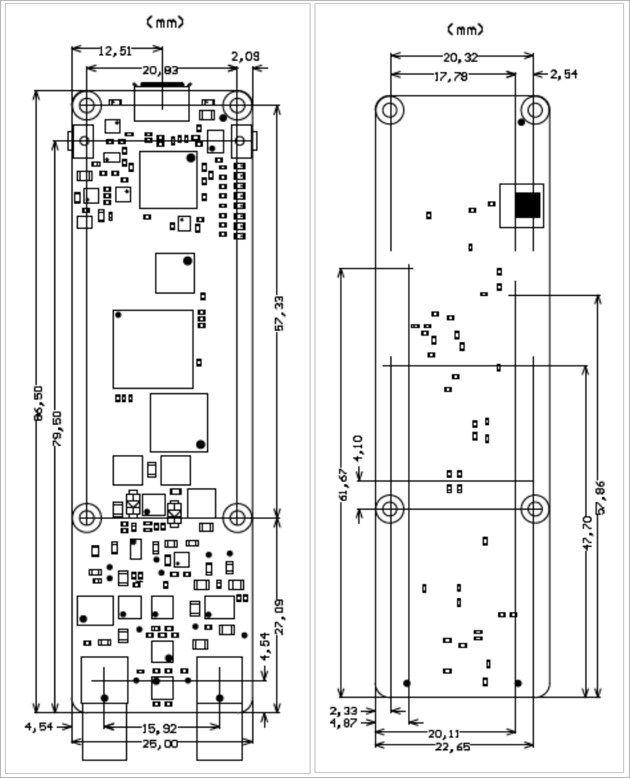 Image Added Image Added |
|
Currently Offered Variants
...