some sources available on public doc TEBT0808 TRM
| Page properties |
|---|
|
Template Revision 2.5
- Module: TRM Name always "TE Series Name" +TRM
Example: "TE0728 TRM" - Carrier: TRM Name usually "TEB Series Name" +TRM
Example: "TEB0728 TRM"
|
...
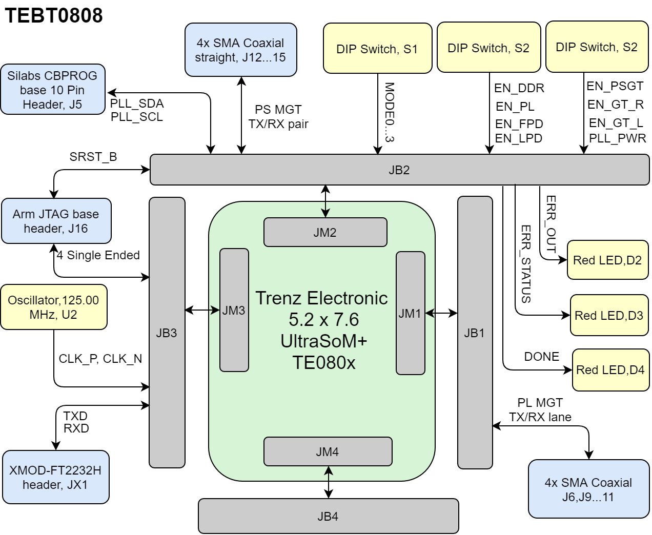
The Trenz Electronic TEBT0808 -01 is a testboard for module TE0808 (REV 02 and 03) as well as for TE0803 (REV 01)test fixture for module TE080x series.
Refer to http://trenz.org/tebt0808-info for the current online version of this manual and other available documentation.
...
...
- Single 3.3V input (Direct modules power supply)
- Header for TE0790 JTAG/UART Adapter
- 20 Pin ARM JTAG header (connected to MIO JTAG 0)
- 10 Pin I2C header for Silabs Clock Builder Field Programmer
- Done, Error/Status LEDs
- One PL GT with SMA connectors
- One PS GT with SMA connectors
- GT local loopback
- PL I/O loopbacks
- PS I/O loopbacks
- Boot Mode switches
- Power control switches to control TE0808 TE080x power domains
- One pre-assembled TE0790 XMOD FTDI JTAG adapter
...
| Scroll Title |
|---|
| anchor | Figure_OV_BD |
|---|
| title | TEBT0808 block diagram |
|---|
|
| Scroll Ignore |
|---|
| draw.io Diagram |
|---|
| border | false |
|---|
| viewerToolbar | true |
|---|
| |
|---|
| fitWindow | false |
|---|
| diagramDisplayName | |
|---|
| lbox | true |
|---|
| revision | 1112 |
|---|
| diagramName | TEBT0808_OV_BD |
|---|
| simpleViewer | false |
|---|
| width | |
|---|
| links | auto |
|---|
| tbstyle | hidden |
|---|
| diagramWidth | 640 |
|---|
|
|
| Scroll Only |
|---|
|
|
...
| Scroll Title |
|---|
| anchor | Table_OV_BP |
|---|
| title | Boot process. |
|---|
|
| Scroll Table Layout |
|---|
| orientation | portrait |
|---|
| sortDirection | ASC |
|---|
| repeatTableHeaders | default |
|---|
| style | |
|---|
| widths | |
|---|
| sortByColumn | 1 |
|---|
| sortEnabled | false |
|---|
| cellHighlighting | true |
|---|
|
| M3 | M2 | M1 | M0 | Bootmode Hex | Bootmode | Notes |
|---|
| ON | ON | ON | ON | 0x0 | PS Main JTAG (TE0790 USB JTAG) | Needed for SPI Flash Programming |
| | ON | ON | OFF | ON | 0x2 | SPI Flash (dual parallel, 4bit x 2, 32bit Addressing)Default |
| | ON | OFF | OFF | OFF | 0x8 | PJTAG(MIO29:26) |
|
|
| Scroll Title |
|---|
| anchor | Table_OV_RST |
|---|
| title | Reset process. |
|---|
|
| Scroll Table Layout |
|---|
| orientation | portrait |
|---|
| sortDirection | ASC |
|---|
| repeatTableHeaders | default |
|---|
| style | |
|---|
| widths | |
|---|
| sortByColumn | 1 |
|---|
| sortEnabled | false |
|---|
| cellHighlighting | true |
|---|
|
Signal | B2B | Note |
|---|
PLL_RST | J2-89 |
| | SRST_B | J2-96 | connected to PJTAG0_SRST - J16 |
|
...
| Scroll Title |
|---|
| anchor | Table_SIP_B2B |
|---|
| title | General PL I/O to B2B connectors information |
|---|
|
| Scroll Table Layout |
|---|
| orientation | portrait |
|---|
| sortDirection | ASC |
|---|
| repeatTableHeaders | default |
|---|
| style | |
|---|
| widths | |
|---|
| sortByColumn | 1 |
|---|
| sortEnabled | false |
|---|
| cellHighlighting | true |
|---|
|
| B2B Connector | Interfaces | Number of I/O | Notes |
|---|
J1
| User I/O | 22 singel ended, 11 Differential 8 singel ended, 4 Differential 8 singel ended, 4 Differential 8 singel ended, 4 Differential 3 singel ended | Connected to Bank 66 Connected to Bank 228 Connected to Bank 229 Connected to Bank 230 VCCO_66, PL_1V8 | J2
| Ethernet PHY | 32 singel ended, 16 Differential 4 singel ended, 16 Differential | Connected to Bank 505 Connected to Bank 128 | | Control Signals | 15 single ended | PLL_SEL0, PLL_SEL1, PLL_RST, EN_GTR, EN_PL, PLL_LOLN, EN_PSGT, ERR_STATUS, ERR_OUT,SRST_B, INIT_B, PROG_B, EN_FPD , EN_LPD , DONE | | Power Control Signal | 10 single ended | EN_PLL_PWR, PLL_FINC ,PG_PLL_1V8, LP_GOOD, PG_DDR, PG_PL, PG_FPD, PG_PSGT, PG_GT_R, PG_GT_L | | JTAG Interface | 7 single ended | TCK, TDI, TMS, TDO, MR, Rxd, Txd | | WANNE2 | 2 single ended | PLL_SCL, PLL_SDA | | Clock | 6 singel ended, 3 Differential | CLK0, CLK7, CLK8 | J3
| User I/O | 12 singel ended, 6 Differential 12 singel ended, 6 Differential | Connected to Bank 48 Connected to Bank 47 | | Clock | 6 singel ended, 3 Differential | CLK228, CLK229, CLK230 | | PJTAG Interface | 7 single ended | PJTAG0_TCK, PJTAG0_TDI, PJTAG0_TMS, PJTAG0_TDO, | | MIO | 27 single ended | MIO19..76 | | UART | 2 single ended | TXD, RXD | | Power pins | 4 single ended | PS_1V8, SI_PLL_1V8, VCCO_48, VCCO_47 | | J4 | User I/O | 48 singel ended, 62 Differential 4 single ended | Connected to Bank 64 Connected to Bank 64 | | Power pins | 4 single ended | VCCO_64, VCCO65 |
|
XMOD JTAG
...
JTAG access to the TE0803 or TE0808 SoM TE080x UltraSoM+ through B2B connector JM2.
...
| anchor | Table_SIP_JTG |
|---|
| title | JTAG pins connection |
|---|
...
JTAG Signal
...
B2B Connector
...
J2-120
...
On-board Peripherals
| Page properties |
|---|
|
Notes : - add subsection for every component which is important for design, for example:
- Two 100 Mbit Ethernet Transciever PHY
- USB PHY
- Programmable Clock Generator
- Oscillators
- eMMCs
- RTC
- FTDI
- ...
- DIP-Switches
- Buttons
- LEDs
|
...
Notes :
...
TODO XMOD Pin Header and recommended XMOD DIP setting and used MIO on B2B connector
PJTAG
TODO Pin Header
TODO Pin Header
SMA
TODO Pin Header
Test Points
TODO List of all Test points with connection
On-board Peripherals
| Page properties |
|---|
|
Notes : - add subsection for every component which is important for design, for example:
- Two 100 Mbit Ethernet Transciever PHY
- USB PHY
- Programmable Clock Generator
- Oscillators
- eMMCs
- RTC
- FTDI
- ...
- DIP-Switches
- Buttons
- LEDs
|
| Page properties |
|---|
|
Notes : In the on-board peripheral table "chip/Interface" must be linked to the corresponding chapter or subsection |
| Scroll Title |
|---|
| anchor | Table_OBP |
|---|
| title | On board peripherals |
|---|
|
| Scroll Table Layout |
|---|
| orientation | portrait |
|---|
| sortDirection | ASC |
|---|
| repeatTableHeaders | default |
|---|
| style | |
|---|
| widths | |
|---|
| sortByColumn | 1 |
|---|
| sortEnabled | false |
|---|
| cellHighlighting | true |
|---|
|
| Chip/Interface | Designator | Notes |
|---|
| Oscillator | U2 | 125.00 MHz |
|
DIP Switch
There are thre DIP Switches, S1, S2, S3.
The Boot Mode can be set through DIP Switch S1, refer to BootMode table.
| Scroll Title |
|---|
| anchor | Table_OBP_DIP |
|---|
| title | On board peripheralsDIP Switch S1 |
|---|
|
| Scroll Table Layout |
|---|
| orientation | portrait |
|---|
| sortDirection | ASC |
|---|
| repeatTableHeaders | default |
|---|
| style | |
|---|
| widths | |
|---|
| sortByColumn | 1 |
|---|
| sortEnabled | false |
|---|
| cellHighlighting | true |
|---|
|
|
...
There are thre DIP Switches, S1, S2, S3.
...
| J2-109 | S1A |
| | MODE1 | J2-107 | S1B |
| | MODE2 | J2-105 | S1C |
| | MODE3 | J2-103 | S1D |
|
|
Control signals must be set by DIP Switch S2, S3.
| Scroll Title |
|---|
| anchor | Table_OBP_DIP |
|---|
| title | DIP Switch S1S2 |
|---|
|
| Scroll Table Layout |
|---|
| orientation | portrait |
|---|
| sortDirection | ASC |
|---|
| repeatTableHeaders | default |
|---|
| style | |
|---|
| widths | |
|---|
| sortByColumn | 1 |
|---|
| sortEnabled | false |
|---|
| cellHighlighting | true |
|---|
|
| Signals | B2B | S1 S2 switch | Notes |
|---|
| MODE0EN_PSGT | J2-10984 | S1A | S2A |
| | EN_GT_RMODE1 | J2-10795 | S1B | S2B |
| | EN_GT_LMODE2 | J2-10597 | S1C | S2C |
| | EN_PLL_PWRMODE3 | J2-10377 | S1D |
|
...
| Scroll Title |
|---|
| anchor | Table_OBP_DIP |
|---|
| title | DIP Switch S2S3 |
|---|
|
| Scroll Table Layout |
|---|
| orientation | portrait |
|---|
| sortDirection | ASC |
|---|
| repeatTableHeaders | default |
|---|
| style | |
|---|
| widths | |
|---|
| sortByColumn | 1 |
|---|
| sortEnabled | false |
|---|
| cellHighlighting | true |
|---|
|
| Signals | B2B | S2 S3 switch | Notes |
|---|
| EN_PSGTDDR | J2-84112 | S2AS3A |
| | EN_GT_RLPD | J2-95108 | S2BS3B |
| | EN_GT_LPL | J2-97101 | S2CS3C |
| | EN_PLL_PWRFPD | J2-77102 | S2D | connected to PG_PLS3D |
|
|
LEDs
| Scroll Title |
|---|
| anchor | Table_OBP_DIPLED |
|---|
| title | DIP Switch S3On-board LEDs |
|---|
|
| Scroll Table Layout |
|---|
| orientation | portrait |
|---|
| sortDirection | ASC |
|---|
| repeatTableHeaders | default |
|---|
| style | |
|---|
| widths | |
|---|
| sortByColumn | 1 |
|---|
| sortEnabled | false |
|---|
| cellHighlighting | true |
|---|
|
| Designator | SignalsColor | B2B | S3 switch | Notes | EN_DDR | J2-112 | S3A | EN_LPD | J2-108 | S3B | EN_PL | J2-101 | S3C | EN_FPD | J2-102 | S3D |
|---|
|
LEDs
| Connected to | Active Level | Note |
|---|
| D2 | Red | DONE | Low |
| | D3 | Red | ERR_STATUS | Low |
| | D4 | Red | ERR_OUT | Low |
|
|
Clock Sources
| Scroll Title |
|---|
| anchor | Table_OBP_LEDCLK |
|---|
| title | On-board LEDs | Osillators |
|---|
|
| scroll-scroll-tablelayout |
|---|
| orientation | portrait |
|---|
| sortDirection | ASC |
|---|
| repeatTableHeaders | default |
|---|
| style | |
|---|
| widths | |
|---|
| sortByColumn | 1 |
|---|
| sortEnabled | false |
|---|
| cellHighlighting | true |
|---|
|
| Designator | ColorDescription | Connected toFrequency | Active Level | Note |
|---|
| D2U2 | Red | DONE | Low | D3 | Red | ERR_STATUS | Low | D4 | Red | ERR_OUT | Low |
|
...
| MEMS Oscillator | 125.00 MHz |
|
|
Power and Power-On Sequence
| Page properties |
|---|
|
In 'Power and Power-on Sequence' section there are three important digrams which must be drawn: - Power on-sequence
- Power distribution
- Voltage monitoring circuit
|
Power Supply
| Scroll Title |
|---|
| anchor | Table_OBPPWR_CLKPC |
|---|
| title | OsillatorsPower Consumption |
|---|
|
| Scroll Table Layout |
|---|
| orientation | portrait |
|---|
| sortDirection | ASC |
|---|
| repeatTableHeaders | default |
|---|
| style | |
|---|
| widths | |
|---|
| sortByColumn | 1 |
|---|
| sortEnabled | false |
|---|
| cellHighlighting | true |
|---|
|
| Designator | Description | Frequency2,0mm MC LB2 | Note | U2 | MEMS Oscillator | 125.00 MHz |
|---|
|
Power and Power-On Sequence
...
In 'Power and Power-on Sequence' section there are three important digrams which must be drawn:
- Power on-sequence
- Power distribution
- Voltage monitoring circuit
| Note |
|---|
For more information regarding how to draw diagram, Please refer to "Diagram Drawing Guidline" . |
| J7 | 3.3V direct modules power supply | | J8 | GND |
|
Current depends manly on design and cooling solution. Use Xilinx Power Estimator and/or Your Vivado Project to estimate min current. Minimum of 3A are recommanded for basic functionality.
Power Consumption
Current depends manly on design and cooling solution. Use Xilinx Power Estimator and/or Your Vivado Project to estimate min current. Minimum of 3A are recommanded for basic functionality.
| Scroll Title |
|---|
| anchor | Table_PWR_PC |
|---|
| title | Power Consumption |
|---|
|
| Scroll Table Layout |
|---|
| orientation | portrait |
|---|
| sortDirection | ASC |
|---|
| repeatTableHeaders | default |
|---|
| style | |
|---|
| widths | |
|---|
| sortByColumn | 1 |
|---|
| sortEnabled | false |
|---|
| cellHighlighting | true |
|---|
|
| Power Input Pin | Typical Current |
|---|
| VIN | TBD* |
|
* TBD - To Be Determined
Power Distribution Dependencies
Input oower sourced directly the module, Only one Diode D1 is used for protection.
Power Supply
TestKits are pre-assembled and pre-flashed with initial Flash image, they start up as soon as power (3.3V) is applied.
Power Consumption
| Scroll Title |
|---|
| anchor | TableFigure_PWR_PCPD |
|---|
| title | Power ConsumptionDistribution |
|---|
|
tablelayout |
| orientation | portrait |
|---|
| sortDirection | ASC |
|---|
| repeatTableHeaders | default |
|---|
style | widths | | sortByColumn | 1 |
|---|
| sortEnabled | false |
|---|
| cellHighlighting | true |
|---|
| Power Input Pin | Typical Current |
|---|
| VIN | TBD* |
* TBD - To Be Determined
Power Distribution Dependencies
If you connect the power supply with wrong polarity, Diod D1 protects the board not to be damaged.
...
| anchor | Figure_PWR_PD |
|---|
| title | Power Distribution |
|---|
| ignore |
|---|
| draw.io Diagram |
|---|
| border | false |
|---|
| viewerToolbar | true |
|---|
| |
|---|
| fitWindow | false |
|---|
| diagramDisplayName | |
|---|
| lbox | true |
|---|
| revision | 2 |
|---|
| diagramName | TEBT0808_PWR_PD |
|---|
| simpleViewer | false |
|---|
| width | |
|---|
| links | auto |
|---|
| tbstyle | hidden |
|---|
| diagramWidth | 640 |
|---|
|
|
| Scroll Only |
|---|
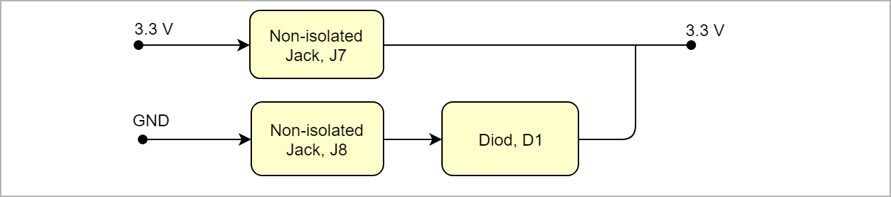 Image Added Image Added
|
|
Power Rails
| Scroll Title |
|---|
| anchor | Table_PWR_PR |
|---|
| title | Module power rails. |
|---|
|
| Scroll Table Layout |
|---|
| orientation | portrait |
|---|
| sortDirection | ASC |
|---|
| repeatTableHeaders | default |
|---|
| style | |
|---|
| widths | |
|---|
| sortByColumn | 1 |
|---|
| sortEnabled | false |
|---|
| cellHighlighting | true |
|---|
|
| Power Rail Name | B2B JM1 Pin | B2B JM2 Pin | B2B JM3 Pin | B2B JM4 Pin | Direction | Notes |
|---|
| 3.3V | 151,153,155,157,159 | 140,142,144,146,156,158,160,
153,155,157,159 | 157,158,159,160 | - | Output | Carrier power supply to module power rails PL_DCDCIN. DCDCIN, LP_DCDC, GT_DCDC, PL_3V3V | VCCO_47 | - | - | 43, 44 | - | Output | Connected to 1.8 (SI_PLL_1V8) | | VCCO_48 | - | - | 15,16 | - | Output | Connected to 1.8 (SI_PLL_1V8) | | VCCO_64 | - | - | - | 58, 106 | Output | Connected to 1.8 (PL_1V8) | | VCCO_65 | - | - | - | 69, 105 | Output | Connected to 1.8 (PL_1V8) |
|
...
| Scroll Only |
|---|
Image Removed |
Power Rails
| Scroll Title |
|---|
| anchor | Table_PWR_PR |
|---|
| title | Module power rails. |
|---|
|
| Scroll Table Layout |
|---|
|
| orientation | portrait |
|---|
| sortDirection | ASC |
|---|
| repeatTableHeaders | default |
|---|
style | widths | | sortByColumn | 1 |
|---|
| sortEnabled | false |
|---|
| cellHighlighting | true |
|---|
| Power Rail Name | B2B JM1 Pin | B2B JM2 Pin | B2B JM3 Pin | B2B JM4 Pin | Direction | Notes |
| VCCO_66 | 90,120 | - | - | - | Output | Connected to 1.8 (PL_1V8) |
3.3V138...160 | -PSBATT125-Connected to 1.8 (PS_1V8) | VCCO_47 | - | - | 43, 44 | - | Output | Connected to SI_PLL_1V8 |
VCCO_48Connected to 15,16 | - | Output | _1V8PS147, 148Output | PLL_3V3152Output | 3.3V | VCCO_6458,106 | 1.8 (PL_1V8)VCCO_6569,105 | Output | | Output | 1.2V..1.5V, abs. max 2V |
Connected to 1.8 (PL_1V8)
Board to Board Connectors
...
| Scroll Title |
|---|
| anchor | Table_TS_AMR |
|---|
| title | PS absolute maximum ratings |
|---|
|
| Scroll Table Layout |
|---|
| orientation | portrait |
|---|
| sortDirection | ASC |
|---|
| repeatTableHeaders | default |
|---|
| style | |
|---|
| widths | |
|---|
| sortByColumn | 1 |
|---|
| sortEnabled | false |
|---|
| cellHighlighting | true |
|---|
|
| Symbols | Min | Max | Unit | Note |
|---|
| VIN | -03.3 | 4 | V | Limit by DC1123, Note: VIN is connected directly to module, this is not considered here Input Supply Voltage | | Storage Temperatur | -40 | +85 | °C |
|
|
...
| Scroll Title |
|---|
| anchor | Table_TS_ROC |
|---|
| title | Recommended operating conditions. |
|---|
|
| Scroll Table Layout |
|---|
| orientation | portrait |
|---|
| sortDirection | ASC |
|---|
| repeatTableHeaders | default |
|---|
| style | |
|---|
| widths | |
|---|
| sortByColumn | 1 |
|---|
| sortEnabled | false |
|---|
| cellHighlighting | true |
|---|
|
| Symbols | Min | Max | Unit | Note |
|---|
| VIN0 | 3,14 | 3.347 | V | Input Supply Voltage | Storage Temperatur | -40 | +85 | °C | Important, check also TRM of the connected module |
|
Physical Dimensions
Module size: 90 mm × 90 mm. Please download the assembly diagram for exact numbers.
Mating height with standard connectors: 3.5 mm.
...
| Scroll Title |
|---|
| anchor | Table_VCP_SO |
|---|
| title | Trenz Electronic Shop Overview |
|---|
|
| Scroll Table Layout |
|---|
| orientation | portrait |
|---|
| sortDirection | ASC |
|---|
| repeatTableHeaders | default |
|---|
| style | |
|---|
| widths | |
|---|
| sortByColumn | 1 |
|---|
| sortEnabled | false |
|---|
| cellHighlighting | true |
|---|
|
|
Revision History
Hardware Revision History
| Scroll Title |
|---|
| anchor | Table_RH_HRH |
|---|
| title | Hardware Revision History |
|---|
|
| Scroll Table Layout |
|---|
| orientation | portrait |
|---|
| sortDirection | ASC |
|---|
| repeatTableHeaders | default |
|---|
| style | |
|---|
| widths | |
|---|
| sortByColumn | 1 |
|---|
| sortEnabled | false |
|---|
| cellHighlighting | true |
|---|
|
| Date | Revision | Changes |
|---|
| 2016-ß6-29 | 01 | - |
|
Document Change History
...