...
| Scroll pdf ignore |
|---|
Table of Contents |
Overview
The Cyclone10 Cyclone 10 LP Reference Kit is the world's first development board with a 55kLE 55 kLE (Logic Elements) Intel Cyclone 10 LP and a variety of interfaces for numerous applications. The board is comprehensively tested and ready for use with end products and can also be ordered in customer-specific variants according to your requirements.
...
| Page properties |
|---|
|
Note:
'Key Features' description: Important components and connector or other Features of the module
→ please sort and indicate assembly options |
- Intel® Intel Cyclone 10 LP LP [10CL055YU484C8G],
- Package: UBGA-484
- Speed Grade: 8 (Slowest)
- Temperature: 0°C ~ 85°C 0 °C to 85° C
- Package compatible device 10CL016, 10CL040, 10CL055, 10CL080 as assembly variant on request is possible
- 16 MBit flash memory (2 MByte) Flash Memory (optional up to 32 MBit possibleMBit (4 MByte))
- Integrated USB2.0 USB-JTAG Programmer
- Pin Header connectorsConnectors
- 256 64 MBit (8 MByte) SDRAM (optional up to 512 MBit possible(64 MByte)) SDRAM
- 128 64 MBit (optional up to 512 MBit possible8 MByte) User Quad-SPI Flash memoryMemory (optional up to 128 MBit (16 MByte))
- 64 MBit (8 MByte) HyperRAM (Pseudo SRAM) (optional up to 128 MBit possible(16 MByte))
- FTDI - System Controller (CPLD)
- 2x MAC address 2x MAC Address EEPROM
- 2x Fast Ethernet PHY (10/100 Mbps)
- 8-channelChannel, 12-bitBit, configurable ADC/DAC with on-chip reference
- D-Sub connectorConnector
- 2x RJ45 connectorConnector
- LEDs:
- Status LEDs, Power LED
- 13x User LEDs
- 7-segment displaySegment Display
- Push bottunsButtons:
- 2x Reset Push buttonsButtons
- 5x User Push buttonsButtons
- I/O: 70 GPIO: 321
- 5 V Power Supply
- LVDS: 132
Power Supply: - 5 V
Minimum 1A
- Dimension: 95 mm x 110 mm
- Others:
- Reverse polarity of supply voltage protectionUnder/Over voltage protectionSupply Protection
- Undervoltage/Overvoltage Protection
Block Diagram
| Page properties |
|---|
|
add drawIO object here.
|
...
| Scroll Title |
|---|
| anchor | Figure_OV_BD |
|---|
| title | TEI0009 block diagramBlock Diagram |
|---|
|
| Scroll Ignore |
|---|
| draw.io Diagram |
|---|
| border | false |
|---|
| viewerToolbar | true |
|---|
| |
|---|
| fitWindow | false |
|---|
| diagramDisplayName | |
|---|
| lbox | true |
|---|
| revision | 817 |
|---|
| diagramName | TEI0009_OV_BD |
|---|
| simpleViewer | false |
|---|
| width | |
|---|
| links | auto |
|---|
| tbstyle | hidden |
|---|
| diagramWidth | 641640 |
|---|
|
|
| Scroll Only |
|---|

|
|
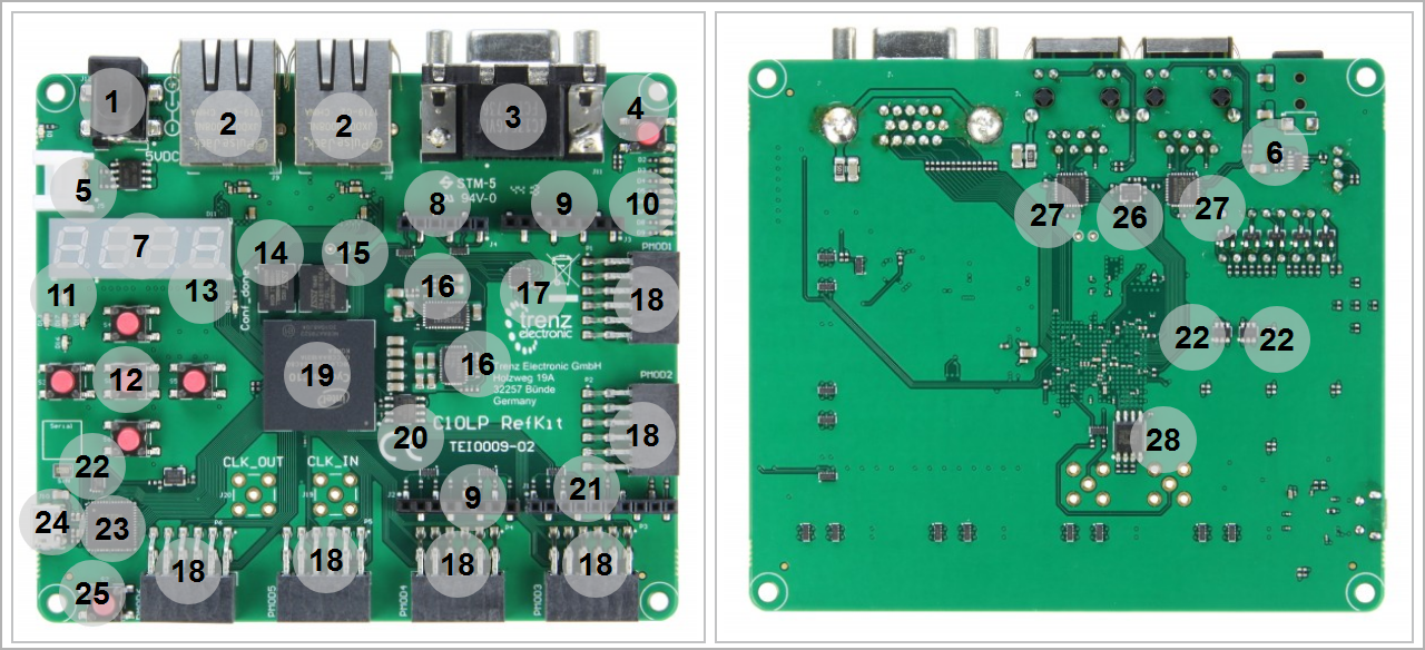
Main Components
...
| Scroll Title |
|---|
| anchor | Figure_OV_BD |
|---|
| title | TEI0009 main componentsMain Components |
|---|
|
| Scroll Ignore |
|---|
| draw.io Diagram |
|---|
| border | false |
|---|
| viewerToolbar | true |
|---|
| |
|---|
| fitWindow | false |
|---|
| diagramDisplayName | |
|---|
| lbox | true |
|---|
| revision | 47 |
|---|
| diagramName | TEI0009_OV_MC |
|---|
| simpleViewer | false |
|---|
| width | |
|---|
| links | auto |
|---|
| tbstyle | hidden |
|---|
| diagramWidth | 640 |
|---|
|
|
| Scroll Only |
|---|
|
|
- Barrel Power Jack, J12
- RJ45 socketSocket, J8...9
- D-Sub Connector, J11
- Push buttonButton (Reset), S7
- Grove connectorConnector, J5
- Under/Over Voltage ProtecterUndervoltage/Overvoltage Protector, U9
- 7-segment Segment LED, D11
- 1x6 pin headerPin Header, J4
- 1x8 pin headerPin Header, J2...3
- 8x User LEDs (Red LEDs), D2...9
- 8x 5x User LEDs (Red LEDs), D13...17
- 5x User Push buttonsButtons, S1 - S3...6
- Red LED (CONF_DONE), D10
- PSRAM memoryMemory, U3
- SDRAM memoryMemory, U10
- Voltage Regulator, U5U4 - U7
- AD/DA ConvertorConverter, U2
- Pmod 2x6 SMD host socket6x Pmod Host Socket, P1...6
- Intel ® Cyclone 10 LP, U1
- Serial Configuration memoryMemory, U5
- 1x10 pin headerPin Header, J1
- EEEPROMEEPROM, U15 - U18 - U20
- FTDI USB2 USB 2 to JTAG/UART adapterConverter, U14
- Micro USB 2.0 (receptacle) , J10
- Push button Button (RST_GPIO), S2
- Oscillator, U22
- Ethernet PHY, U17 - U19
- QSPI Flash memoryMemory, U12
Initial Delivery State
| Page properties |
|---|
|
Notes : Only components like EEPROM, QSPI flash and DDR3 can be initialized by default at manufacture. If there is no components which might have initial data ( possible on carrier) you must keep the table empty |
...
| Scroll Title |
|---|
| anchor | Table_OV_IDS |
|---|
| title | Initial delivery state of programmable devices Delivery State of Programmable Devices on the moduleModule |
|---|
|
| Scroll Table Layout |
|---|
| orientation | portrait |
|---|
| sortDirection | ASC |
|---|
| repeatTableHeaders | default |
|---|
| style | |
|---|
| widths | |
|---|
| sortByColumn | 1 |
|---|
| sortEnabled | false |
|---|
| cellHighlighting | true |
|---|
|
Storage device name | Content | Notes |
|---|
QSPI Flash (U12) | Not programmed |
| | EEPROM (U15) | Programmed | FTDI configurationConfiguration | | EEPROM (U18, U20)SDRAM | Not programmed | Except Ethernet MAC | | SDRAM (U10) | Not programmed |
| | PSRAM (U3) | PSRAM | Not programmed | FTDI System Controller CPLD | Not programmed |
| | Serial Configuration Memory (U5) | Demo DesignProgrammed |
|
|
Configuration Signals
| Page properties |
|---|
|
- Overview of Boot Mode, Reset, Enables.
|
...
| Scroll Title |
|---|
| anchor | Table_OV_BP |
|---|
| title | Boot process.Process |
|---|
|
| Scroll Table Layout |
|---|
| orientation | portrait |
|---|
| sortDirection | ASC |
|---|
| repeatTableHeaders | default |
|---|
| style | |
|---|
| widths | |
|---|
| sortByColumn | 1 |
|---|
| sortEnabled | false |
|---|
| cellHighlighting | true |
|---|
|
MODE Signal State | MSEL0 | MSEL1 | MSEL2 | MSEL3 | Connected to | Boot Mode |
|---|
MSEL[0:3] | 0 | 1 | 0 | 0 | Bank 6 | AS (Active Serial) |
|
RESET pin can be set through the push button S1.
| Scroll Title |
|---|
| anchor | Table_OV_RST |
|---|
| title | Reset process.Process |
|---|
|
| Scroll Table Layout |
|---|
| orientation | portrait |
|---|
| sortDirection | ASC |
|---|
| repeatTableHeaders | default |
|---|
| style | |
|---|
| widths | |
|---|
| sortByColumn | 1 |
|---|
| sortEnabled | false |
|---|
| cellHighlighting | true |
|---|
|
Signal | Connected to | Note |
|---|
RESET | S7 (Push button)S7, Push Button | Connected to nCONFIG | RST_GPIO | S2 (Push button) | EXT_RST | J3 (1x8 pin header) Bank 2. |
|
Signals, Interfaces and Pins
...
FPGA bank number and number of I/O signals connected to the B2B connectorconnectors:
| Scroll Title |
|---|
| anchor | Table_SIP_B2B |
|---|
| title | General I/O to Pin header Header and Pmod SMD connectors informationConnectors Information |
|---|
|
| Scroll Table Layout |
|---|
| orientation | portrait |
|---|
| sortDirection | ASC |
|---|
| repeatTableHeaders | default |
|---|
| style | |
|---|
| widths | |
|---|
| sortByColumn | 1 |
|---|
| sortEnabled | false |
|---|
| cellHighlighting | true |
|---|
|
| FPGA Bank | Connector | I/O Signal Count | Voltage Level | Notes |
|---|
| Bank 1 | J1 (Pin header) | 8 Single ended | 3.3 V |
| | J2 (Pin header) | 8 Single ended | 3.3 V |
| | J4 (Pin header) | 6 Single ended | 3.3 V |
| | Bank 2 | J3 (Pin header) | 1 Single ended | 3.3 V |
| | P1 (PMod SMD host socketPmod Host Socket) | 8 Single ended | 3.3 V |
| | P2 (PMod SMD host socketPmod Host Socket) | 8 Single ended | 3.3 V |
| | J11 (VGA host Host Socket) | 14 Single ended | 3.3 V |
| | Bank 6 | J5 (Grove connectorConnector) | 2 Single ended | 3.3 V |
| | Bank 7 | P5 (PMod SMD host socketPmod Host Socket) | 8 Single ended | 3.3 V |
| | P6 (PMod SMD host socketPmod Host Socket) | 8 Single ended | 3.3 V |
| | Bank 8 | P3 (PMod SMD host socketPmod Host Socket) | 8 Single ended | 3.3 V |
| | P4 (PMod SMD host socketPmod Host Socket) | 8 Single ended | 3.3 V |
|
...
Pmod Host Socket
TEI0009 has 6 PMod 2x6 SMD Host Socket 90° 6 Pmod 2x6 host sockets which are connected to Cyclon 10 LP (U1).
| Scroll Title |
|---|
| anchor | Table_SIP_SMD |
|---|
| title | PMod SMD host socket informationPmod SMD Host Socket Information |
|---|
|
| Scroll Table Layout |
|---|
| orientation | portrait |
|---|
| sortDirection | ASC |
|---|
| repeatTableHeaders | default |
|---|
| style | |
|---|
| widths | |
|---|
| sortByColumn | 1 |
|---|
| sortEnabled | false |
|---|
| cellHighlighting | true |
|---|
|
| Designator | Signals | Connected to | Notes |
|---|
| P1 | P1_IO1...8 | Bank 2 |
| | P2 | P2_IO1...8 | Bank 2 |
| | P3 | P3_IO1...8 | Bank 8 |
| | P4 | P4_IO1...8 | Bank 8 |
| | P5 | P5_IO1...8 | Bank 7 |
| | P6 | P6_IO1...8 | Bank 7 |
|
UART Interface
UART access to TEI0009 is available on 1x8 pin header J2.
...
| anchor | Table_SIP_UART |
|---|
| title | UART interface information |
|---|
TEI0009 has 5 pin headers. The pin headers J1...4 are usable for Arduino modules, too.
| Scroll Table Layout |
|---|
| orientation | portrait |
|---|
| sortDirection |
|---|
|
...
| ASC |
|---|
| repeatTableHeaders | default |
|---|
| style | |
|---|
| widths | |
|---|
| sortByColumn | 1 |
|---|
| sortEnabled | false |
|---|
| cellHighlighting | true |
|---|
|
| Scroll Title |
|---|
| anchor | Table_SIP_J1 |
|---|
| title | Pin Header J1 |
|---|
| Schematic |
| Pin Header J1 | Signals | Connected to |
|---|
Voltage Level | TXD | J23.3 V | RXD | |
| | J1 - 7 | GND |
|
| | J1 - 8 | AREF | ADC/DAC |
| | J1 - 9 | D14_SDA |
J23.3 V | |
Micro USB2.0 Connector
...
| Scroll Title |
|---|
| anchor | Table_SIP_USBJ2 |
|---|
| title | Micro USB2.0 B Receptacle 90 ° informationPin Header J2 |
|---|
|
| Scroll Table Layout |
|---|
| orientation | portrait |
|---|
| sortDirection | ASC |
|---|
| repeatTableHeaders | default |
|---|
| style | |
|---|
| widths | |
|---|
| sortByColumn | 1 |
|---|
| sortEnabled | false |
|---|
| cellHighlighting | true |
|---|
|
Schematic| Voltage Level | Notes | USB_VBUS | GND | D- | U14 (FTDI FT2232) | 3.3 V | D+ | U14 (FTDI FT2232) | 3.3 V | |
RJ45 Connectors
TEI0009 is equipped with two RJ45 connectors and two Ethernet PHYs. RJ45 connectors J8 and J9 are connected to Ethernet PHYs U17 and U19 respectively. .
| Notes |
|---|
| J2 - 1 | D0_RXD | Bank 1 |
| | J2 - 2 | D1_TXD | Bank 1 |
| | J2 - 3...8 | D2...4 | Bank 1 |
|
|
| scrollscroll-title |
|---|
| anchor | Table_SIP_RJ45J3 |
|---|
| title | RJ45 connectors informationPin Header J3 |
|---|
|
| Scroll Table Layout |
|---|
| orientation | portrait |
|---|
| sortDirection | ASC |
|---|
| repeatTableHeaders | default |
|---|
| style | |
|---|
| widths | |
|---|
| sortByColumn | 1 |
|---|
| sortEnabled | false |
|---|
| cellHighlighting | true |
|---|
|
| Schematic | ETH1 Pin | ETH2 PinTD+ | ETH_TX_P | U17- TXP | U19- TXP | | CT | ETH_CTREF_TCT | - | - | Connected to GND | TD- | ETH_TX_N | U17- TXM | U19- TXM | RD+ | ETH_RX_P | U17- RXP | U19- RXP | | CT | ETH_CTREF_RCT | - | - | Connected to GND | RD- | ETH_RX_N | U17- RXM | U19- RXM | LED Green | ETH_LED0 | U17- NWAYEN | U19- NWAYEN | LED Yellow | ETH_LED1 | U17- SPEED | U19- SPEED | |
D-Sub Connectors
TEI0009 is equipped with a D-Sub connector (Receptacle) which provides interface to Cyclone 10 LP through Bank 2.
| J2 - 1 | NC | - |
| | J3 - 2 | 3.3V | 3.3 V |
| | J3 - 3 | EXT_RST | Bank 2 | Pulled-up to 3.3 V | | J3 - 4 | 3.3V | 3.3 V |
| | J3 - 5 | 5V | 5 V |
| | J3 - 6...7 | GND | GND |
| | J2 - 8 | NC | - |
|
|
| Scroll Title |
|---|
| anchor | Table_SIP_J4 |
|---|
| title | Pin Header J4 |
|---|
|
|
| Scroll Title |
|---|
| anchor | Table_SIP_VGA |
|---|
| title | VGA host socket information |
|---|
|
| scroll-tablelayout |
|---|
| orientation | portrait |
|---|
| sortDirection | ASC |
|---|
| repeatTableHeaders | default |
|---|
| style | |
|---|
| widths | |
|---|
| sortByColumn | 1 |
|---|
| sortEnabled | false |
|---|
| cellHighlighting | true |
|---|
|
SchematicCorresponding toVGA_R0| VGA_RED | 3Bank 2 | Red channel | | VGA_GREEN | VGA_G0...3 | Bank 2 | Green channel | | VGA_BLUE | VGA_B0...3 | Bank 2 | Blue channel | | VGA_RGB_HSYNC | VGA_HS | Bank 2 | Horizontal sync | | VGA_RGB_VSYNC | VGA_VS | Bank 2 | Vertical sync | |
On-board Peripherals
| 6 | AIN0...5 | FPGA Bank 1 and ADC/DAC |
|
|
| Scroll Title |
|---|
| anchor | Table_SIP_J5 |
|---|
| title | Pin Header J5 |
|---|
|
| Scroll Table Layout |
|---|
| orientation | portrait |
|---|
| sortDirection | ASC |
|---|
| repeatTableHeaders | default |
|---|
| style | |
|---|
| widths | |
|---|
| sortByColumn | 1 |
|---|
| sortEnabled | false |
|---|
| cellHighlighting | true |
|---|
|
| Pin Header J5 | Signals | Connected to | Notes |
|---|
| J5 - 1 | I2C_SCL | FPGA Bank 6 and EEPROM (U18, U20) | Pulled-up to 3.3V. | | J5 - 2 | I2C_SDA | FPGA Bank 6 and EEPROM (U18, U20) | Pulled-up to 3.3V. | | J5 - 3 | 3.3V | 3.3 V |
| | J5 - 4 | GND | GND |
|
|
Micro USB 2.0 Connector
FTDI FT2232 (U14) can be accessed through micro USB 2.0 B connector (J10) for JTAG (channel A). Channel B is connected to the FPGA and can be used for UART or other standards.
RJ45 Connectors
TEI0009 is equipped with two RJ45 connectors and two Ethernet PHYs. RJ45 connectors J8 and J9 are connected to Ethernet PHYs U17 and U19 respectively.
| Scroll Title |
|---|
| anchor | Table_SIP_RJ45 |
|---|
| title | RJ45 Connectors Information |
|---|
|
| Scroll Table Layout |
|---|
| orientation | portrait |
|---|
| sortDirection | ASC |
|---|
| repeatTableHeaders | default |
|---|
| style | |
|---|
| widths | |
|---|
| sortByColumn | 1 |
|---|
| sortEnabled | false |
|---|
| cellHighlighting | true |
|---|
|
| Pin | Schematic | ETH1 Pin | ETH2 Pin | Notes |
|---|
| TD+ | ETH1_TX_P, ETH2_TX_P | U17 - TXP | U19 - TXP |
| | CT | ETH1_CTREF_TCT, ETH2_CTREF_TCT | - | - |
| | TD- | ETH1_TX_N, ETH2_TX_N | U17 - TXM | U19 - TXM |
| | RD+ | ETH1_RX_P, ETH2_RX_P | U17 - RXP | U19 - RXP |
| | CT | ETH1_CTREF_RCT, ETH2_CTREF_RCT | - | - |
| | RD- | ETH1_RX_N, ETH2_RX_N | U17 - RXM | U19 - RXM |
| | LED Green | ETH1_LED0, ETH2_LED0 | U17 - LED0/NWAYEN | U19 - LED0/NWAYEN |
| | LED Yellow | ETH1_LED1, ETH2_LED1 | U17 - LED1/SPEED | U19 - LED1/SPEED |
|
|
D-Sub Connector
TEI0009 is equipped with a D-Sub connector which provides interface to Cyclone 10 LP through Bank 2.
| Scroll Title |
|---|
| anchor | Table_SIP_VGA |
|---|
| title | VGA Host Socket Information |
|---|
|
| Scroll Table Layout |
|---|
| orientation | portrait |
|---|
| sortDirection | ASC |
|---|
| repeatTableHeaders | default |
|---|
| style | |
|---|
| widths | |
|---|
| sortByColumn | 1 |
|---|
| sortEnabled | false |
|---|
| cellHighlighting | true |
|---|
|
| Schematic | Corresponding Signals | Connected to | Notes |
|---|
| VGA_RED | VGA_R0...3 | Bank 2 | Red Channel | | VGA_GREEN | VGA_G0...3 | Bank 2 | Green Channel | | VGA_BLUE | VGA_B0...3 | Bank 2 | Blue Channel | | VGA_RGB_HSYNC | VGA_HS | Bank 2 | Horizontal Sync | | VGA_RGB_VSYNC | VGA_VS | Bank 2 | Vertical Sync |
|
On-board Peripherals
| Page properties |
|---|
|
Notes : - add subsection for every component which is important for design, for example:
- Two 100 Mbit Ethernet Transciever PHY
- USB PHY
- Programmable Clock Generator
- Oscillators
- eMMCs
- RTC
- FTDI
- ...
- DIP-Switches
|
| Page properties |
|---|
|
Notes : - add subsection for every component which is important for design, for example:
- Two 100 Mbit Ethernet Transciever PHY
- USB PHY
- Programmable Clock Generator
- Oscillators
- eMMCs
- RTC
- FTDI
- ...
- DIP-Switches
- Buttons
- LEDs
|
| Page properties |
|---|
|
Notes : In the on-board peripheral table "chip/Interface" must be linked to the corresponding chapter or subsection |
...
| Scroll Title |
|---|
| anchor | Table_OBP |
|---|
| title | On-board peripheralsPeripherals |
|---|
|
| Scroll Table Layout |
|---|
| orientation | portrait |
|---|
| sortDirection | ASC |
|---|
| repeatTableHeaders | default |
|---|
| style | |
|---|
| widths | |
|---|
| sortByColumn | 1 |
|---|
| sortEnabled | false |
|---|
| cellHighlighting | true |
|---|
|
|
QSPI Flash Memory
| Page properties |
|---|
|
Notes : Minimum and Maximum density of quad SPI flash must be mentioned for other assembly options. |
There is a 64MBit 64 MBit (8 MByte) QSPI Flash memory (U12) provided by Winbond Integrated Silicon Solution Inc. which can be used to store data or configuration. Up to 128 MBit (16 MByte) memory is available on other assembly option.
| Scroll Title |
|---|
| anchor | Table_OBP_SPI |
|---|
| title | Quad SPI interface Interface MIOs and pinsPins |
|---|
|
| Scroll Table Layout |
|---|
| orientation | portrait |
|---|
| sortDirection | ASC |
|---|
| repeatTableHeaders | default |
|---|
| style | |
|---|
| widths | |
|---|
| sortByColumn | 1 |
|---|
| sortEnabled | false |
|---|
| cellHighlighting | true |
|---|
|
| Pin | Schematic | Connected to | Notes |
|---|
| CS | F_CS | Bank 7 |
| | CLK | F_CLK | Bank 7 |
| | IO0...3 | F_IO0...3 | Bank 7 |
|
|
...
| Page properties |
|---|
|
Notes : Minimum and Maximum density of DDR3 SDRAM must be mentioned for other assembly options. (pay attention to supported address length for DDR3) |
The TEI0009 has 256 64 MBit (8 MByte) volatile memory provided by Winbond Integrated Silicon Solution Inc., SDRAM IC(U10) for storing user application code and data. Up to 512 MBit (64 MByte) SDRAM is possibleon available on other assembly option.
Part number: W9864G6JTIS42S16400J-6-ND7BL
Supply voltage: 3.3 V
- Clock Frequency: 166MHz143 MHz (optional up to 200 MHz)
Temperature: 0°C ~ 70°Cto 70°C (optional other ranges are available)
PSRAM Memory
The TEI0009 is integrated with 64Mbit 64 Mbit (8 MByte) Pseudo Static Random Access Memory (PSRAM) using a self-refresh DRAM array organized as 8M words by 8 bits. The device supports a HyperBus interface, Very Low Signal Count (Address, Command and data through 8 DQ pins), Hidden Refresh Operation, and Automotive Temperature Operation. Up to 128 MBit (16 MByte) memory is available on other assembly option.
Part number: IS66WVH8M8BLLIS66WVH8M8
Supply voltage: 3.3 V
- Clock Frequency: 100MHz100 MHz
Temperature: -40°C ~ 85°Cto 85°C (optional other ranges are available)
7-Segment
...
Display
The TEI0009 has a LED 4-Digit-7-Segment - 4 Digit LED display which is connected to Bank 6.
| Scroll Title |
|---|
| anchor | Table_OBP_7SEG |
|---|
| title | LED 7-Segment pinsLED Pins |
|---|
|
| Scroll Table Layout |
|---|
| orientation | portrait |
|---|
| sortDirection | ASC |
|---|
| repeatTableHeaders | default |
|---|
| style | |
|---|
| widths | |
|---|
| sortByColumn | 1 |
|---|
| sortEnabled | false |
|---|
| cellHighlighting | true |
|---|
|
| Pin | Schematic | Connected to | Notes |
|---|
| A/L1 | SEG_CA | Bank 6 |
| | B/L2 | SEG_CB | Bank 6 |
| | C/L3 | SEG_CC | Bank 6 |
| | D | SEG_CD | Bank 6 |
| | E | SEG_CE | Bank 6 |
| | F | SEG_CF | Bank 6 |
| | G | SEG_CG | Bank 6 |
| | DP | SEG_CDP | Bank 6 |
| | A1 | SEG_AN | Bank 6 |
| | A2 | SEG_AN4 | Bank 6 |
| | A3 | SEG_AN3 | Bank 6 |
| | A4 | SEG_AN2 | Bank 6 |
| | L1-L3 | SEG_AN1 | Bank 6 |
|
|
...
The FTDI chip U14 converts signals from USB2USB 2.0 to a variety of standard serial and parallel interfaces. Refer to the FTDI data sheet to get for more information about the capacity of the FT2232H chip.
Channel A of FTDI FT2232H chip is used in MPPSE mode for JTAG, 6 I/O's of for JTAG. Channel B are is routed to FPGA bank 8 of the FPGA SoC and are usable for example as GPIOs, UART or 6 and is usable for other standard interfaces.
...
| Scroll Title |
|---|
| anchor | Table_OBP_FTDI |
|---|
| title | FTDI chip interfaces Chip Interfaces and pinsPins |
|---|
|
| Scroll Table Layout |
|---|
| orientation | portrait |
|---|
| sortDirection | ASC |
|---|
| repeatTableHeaders | default |
|---|
| style | |
|---|
| widths | |
|---|
| sortByColumn | 1 |
|---|
| sortEnabled | false |
|---|
| cellHighlighting | true |
|---|
|
| FTDI Chip Pin | Signal Schematic Name | Connected to | Notes |
|---|
| ADBUS0 | TCK | Bank 1 | JTAG interface | | ADBUS1 | TDI | Bank 1 | | ADBUS2 | TDO | Bank 1 | | ADBUS3 | TMS | Bank 1 | | BDBUS0...7 | BDBUS0...7 | Bank 6 |
BDBUS1 | BDBUS1 | Bank 6 | BDBUS2 | BDBUS2 | Bank 6 | BDBUS3 | BDBUS3 | Bank 6 | BDBUS4 | BDBUS4
| | BCBUS0...7 | BCBUS0...7 | Bank 6 |
BDBUS5 | BDBUS5 | Bank 6 | (EEPROM) (EEPROM) (EEPROM)U16 (12MHz Oscillator)| 12 MHz Oscillator, U16 |
| | DM | D_N |
J10 ( USB2)J10 ( USB2)
|
Serial Configuration Memory
On-board serial configuration memory (U5) is provided by Intel with 16 MBit (2 MByte) storage capacity. This non volatile memory is used to store initial FPGA configuration via JTAG interface. The memory is connected to FPGA bank 1 via active serial (AS) x1 interface.
| Scroll Title |
|---|
| anchor | Table_OBP_EEPSCM |
|---|
| title | FTDI and EEPROM pin connectionsSerial Configuration Memory |
|---|
|
| Scroll Table Layout |
|---|
| orientation | portrait |
|---|
| sortDirection | ASC |
|---|
| repeatTableHeaders | default |
|---|
| style | |
|---|
| widths | |
|---|
| sortByColumn | 1 |
|---|
| sortEnabled | false |
|---|
| cellHighlighting | true |
|---|
|
| Configuration Memory Pin | Signal Schematic Name | Connected to | Notes |
|---|
| DATA1 | AS_DATA0 | U1, Bank 1
| Data out
|
| | DATA0 | AS_ASDO | U1, Bank 1 | Data in |
| | nCS | AS_NCSnCS | U1, Bank 1 | chip select |
| | DCLK | AS_DCLK | U1, Bank 1 | clock |
|
|
Ethernet PHY
The TEI0009 is equipped with two Ethernet PHY (U17, U19, U17) which are connected to two RJ45 (J8, J9) connectors.
| Scroll Title |
|---|
| anchor | Table_OBP_ETH |
|---|
| title | Ethernet PHY connections Connections and pinsPins |
|---|
|
| Scroll Table Layout |
|---|
| orientation | portrait |
|---|
| sortDirection | ASC |
|---|
| repeatTableHeaders | default |
|---|
| style | |
|---|
| widths | |
|---|
| sortByColumn | 1 |
|---|
| sortEnabled | false |
|---|
| cellHighlighting | true |
|---|
|
| Ethernet PHY Pin | Signal Schematic Names (ETH1/ETH2) | ETH 1 | ETH 2 | Note |
|---|
| TXD0...3 |
ETH| ETH1_TXD0...3, ETH2_TXD0...3 | Bank 5 | Bank 5 |
| | TXC |
ETH| ETH1_TXC, ETH2_TXC | Bank 5 | Bank 5 |
| | TXEN |
ETH| ETH1_TXEN, ETH2_TXEN | Bank 5 | Bank 5 |
ETH| , ETH2_RXD0...3 | Bank 5 | Bank 5 |
| | RXC |
/ETH| ETH1_RXC, ETH2_RXC | Bank 5 | Bank 5 |
| | RXER/ISO |
ETH| ETH1_RXER, ETH2_RXER | Bank 5 | Bank 5 |
| | INTRP/ |
/NANDETH| ETH1_INTRP, ETH2_INTRP | Bank 5 | Bank 5 |
| | XI |
ETH| ETH1_CLKIN, ETH2_CLKIN | Oscillator, U22 |
() (Oscillator)ETH| ETH1_MDC, ETH2_MDC | Bank 5 | Bank 5 |
| | MDIO |
ETH| ETH1_MDIO, ETH2_MDIO | Bank 5 | Bank 5 |
| | COL/CONFIG0 |
ETH| ETH1_COL, ETH2_COL | Bank 5 | Bank 5 |
| | CRS/CONFIG1 |
ETH| ETH1_CRS, ETH2_CRS | Bank 5 | Bank 5 |
| | RXDV/CONFIG2 |
ETH| ETH1_RXDV, ETH2_RXDV | Bank 5 | Bank 5 |
| | LED0/NWAYEN |
ETHBank 5J8B ()Bank 5 J9B ()ETHBank 5J8C (Bank 5 J9B ())ETH| ETH1_RST, ETH2_RST | Bank 5 | Bank 5 |
| | RXM |
ETH| ETH1_RX_N, ETH2_RX_N | RJ45, J8 |
(RJ45)J9 ()ETHJ8 ()J9 ()ETHJ8 ()J9 ()ETHJ8 ()J9 ()
|
EEPROM
TEI0009 has three EEPROM, U15, U18 and U20. U15 is pre-programmed by for the FTDI FT2232H configuration. U18 and U19 are used for the MAC address configuration.
| Scroll Title |
|---|
| anchor | Table_OBP_EEP |
|---|
| title | FTDI and EEPROM pin connectionsPin Connections |
|---|
|
| Scroll Table Layout |
|---|
| orientation | portrait |
|---|
| sortDirection | ASC |
|---|
| repeatTableHeaders | default |
|---|
| style | |
|---|
| widths | |
|---|
| sortByColumn | 1 |
|---|
| sortEnabled | false |
|---|
| cellHighlighting | true |
|---|
|
| Designator | EEPROM Pin | Signal Schematic Names | Connected to | Notes |
|---|
| U15 | CS | EECS | FTDI, U14 (FTDI) |
| | CLK | |EECLK | FTDI, U14 (FTDI) |
| | DIN/DOUT | EEDATA | FTDI, U14 (FTDI) | FTDI Configuration |
|
|
| Scroll Title |
|---|
| anchor | Table_OBP_EEP |
|---|
| title | I2C EEPROM interface Interface MIOs and pinsPins |
|---|
|
| Scroll Table Layout |
|---|
| orientation | portrait |
|---|
| sortDirection | ASC |
|---|
| repeatTableHeaders | default |
|---|
| style | |
|---|
| widths | |
|---|
| sortByColumn | 1 |
|---|
| sortEnabled | false |
|---|
| cellHighlighting | true |
|---|
|
| Designator | Pin | Schematic | Connected to | Grove Header | Notes |
|---|
| U18, U20 | SCL | I2C_SCL | Bank 6 | J5 |
| | SDA | I2C_SDA | Bank 6 | J5 |
|
|
...
| Scroll Title |
|---|
| anchor | Table_OBP_I2C_EEPROM |
|---|
| title | I2C address Address for EEPROM |
|---|
|
| Scroll Table Layout |
|---|
| orientation | portrait |
|---|
| sortDirection | ASC |
|---|
| repeatTableHeaders | default |
|---|
| style | |
|---|
| widths | |
|---|
| sortByColumn | 1 |
|---|
| sortEnabled | false |
|---|
| cellHighlighting | true |
|---|
|
| I2C Address | Designator | Notes |
|---|
| 0x50 | U18 |
| | 0x520x51 | U20 |
|
|
ADC/DAC
The TEI0009 module is equipped with 12bit a 12-Bit ADC/DAC (U2).
| Scroll Title |
|---|
| anchor | Table_OBP_A2D |
|---|
| title | ADC/DAC interface Interface and pinsPins |
|---|
|
| Scroll Table Layout |
|---|
| orientation | portrait |
|---|
| sortDirection | ASC |
|---|
| repeatTableHeaders | default |
|---|
| style | |
|---|
| widths | |
|---|
| sortByColumn | 1 |
|---|
| sortEnabled | false |
|---|
| cellHighlighting | true |
|---|
|
| Pins | Schematic | Connected to | Notes |
|---|
nRESET | ADDA_RSTN | U1, Bank 2VREF_ADC, U1 |
| | nSYNC | ADDA_SYNC | U1, Bank 2, U1 |
| | SCLK | MCLK | U1, Bank 2, U1 |
| | SDI | MSDIMOSI | U1, Bank 2, U1 |
| | SDO | MSDOMISO | U1, Bank 2, U1 |
| | VREF | -AREF | U1Pin Header, Bank 2J1 | External reference is 1 V to 3.3 V.3V
Internal reference is 2.5 V. | | IO0...5 | AIN0...5 | U1, Bank 1, U1 Pin Header, J4, Pin header |
| | IO6 | AIN6 | Testpoint, TP1 |
| | IO7 | AIN7 | Testpoint, TP2 |
|
|
LEDs
| Scroll Title |
|---|
| anchor | Table_OBP_LED |
|---|
| title | On-board LEDs |
|---|
|
| Scroll Table Layout |
|---|
| orientation | portrait |
|---|
| sortDirection | ASC |
|---|
| repeatTableHeaders | default |
|---|
| style | |
|---|
| widths | |
|---|
| sortByColumn | 1 |
|---|
| sortEnabled | false |
|---|
| cellHighlighting | true |
|---|
|
| Schematic | Designator | Color | Connected to | Active Level | Note |
|---|
| LED1...8 | D2...9 | Red | Bank 3 | High |
| | LED_PB1...5 | D13...17 | Red | Bank 7 | High |
| | CONF_DONE | D10 | Red | Bank 6 | Low |
| | 3.3V | D1 | Green | 3.3V | High |
|
|
Push Buttons
| Scroll Title |
|---|
| anchor | Table_OBP_PBTN |
|---|
| title | On-board Push Buttons |
|---|
|
| Scroll Table Layout |
|---|
| orientation | portrait |
|---|
| sortDirection | ASC |
|---|
| repeatTableHeaders | default |
|---|
| style | |
|---|
| widths |
|---|
| sortByColumn | 1 |
|---|
| sortEnabled | false |
|---|
| cellHighlighting | true |
|---|
| |
|---|
| sortByColumn | 1 |
|---|
| sortEnabled | false |
|---|
| cellHighlighting | true |
|---|
|
| Schematic | Designator | Connected to | Functionality | Note |
|---|
| RESET | S7 | Bank 1 | Reset |
| | RST_GPIO | S2 | Bank 4 | Reset/GPIO |
| | USER_BTN1 | S3 | Bank 3 | User Push Button |
| | USER_BTN2 | S4 | Bank 3 | User Push Button |
| | USER_BTN3 | S5 | Bank 3 | User Push Button |
| | USER_BTN4 | S6 | Bank 3 | User Push Button |
| | USER_BTN5 | S1 | Bank 3 | User Push Button | | Designator | Connected to | Functionality | Note |
|---|
| S7 | RESET | High | S2 | RST_GPIO | High | S1, S3...6 | USER_BTN1...5 | User push buttons | connected to bank 3 |
|
|
Clock Sources
| Scroll Title |
|---|
| anchor | Table_OBP_CLK |
|---|
| title | OsillatorsOscillators |
|---|
|
| Scroll Table Layout |
|---|
| orientation | portrait |
|---|
| sortDirection | ASC |
|---|
| repeatTableHeaders | default |
|---|
| style | |
|---|
| widths | |
|---|
| sortByColumn | 1 |
|---|
| sortEnabled | false |
|---|
| cellHighlighting | true |
|---|
|
| Designator | Description | Frequency | Note |
|---|
| U22 | MEMS Crystal Oscillator | 25 MHz |
| | U16 | MEMS Crystal Oscillator | 12 MHz |
|
|
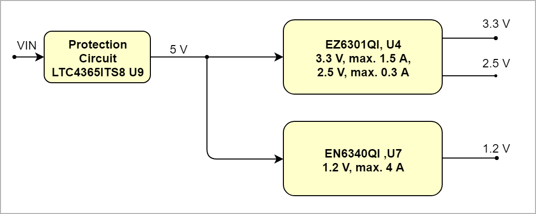
Power and Power-On Sequence
...
Power supply with minimum current capability of 1A 3 A for system startup is recommended.
...
| Scroll Title |
|---|
| anchor | Figure_PWR_PD |
|---|
| title | Power Distribution |
|---|
|
| Scroll Ignore |
|---|
| draw.io Diagram |
|---|
| border | false |
|---|
| viewerToolbar | true |
|---|
| |
|---|
| fitWindow | false |
|---|
| diagramDisplayName | |
|---|
| lbox | true |
|---|
| revision | 711 |
|---|
| diagramName | TEI0009_PWR_PD |
|---|
| simpleViewer | false |
|---|
| width | |
|---|
| links | auto |
|---|
| tbstyle | hidden |
|---|
| diagramWidth | 639540 |
|---|
|
|
| Scroll Only |
|---|
|
|
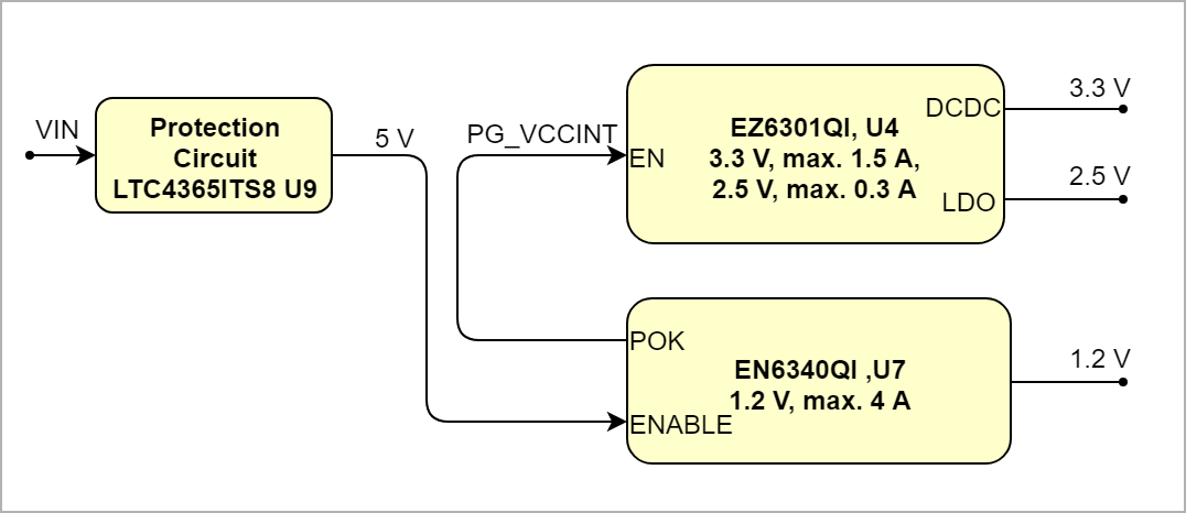
Power-On Sequence
There is no the following power on sequence, After power on, all regulators will be enabled as you can see in -on sequence. The DCDC converter U7 enables the device U4 according to the diagram below.
| Scroll Title |
|---|
| anchor | Figure_PWR_PS |
|---|
| title | Power Sequency |
|---|
|
| Scroll Ignore |
|---|
| draw.io Diagram |
|---|
| border | false |
|---|
| viewerToolbar | true |
|---|
| |
|---|
| fitWindow | false |
|---|
| diagramDisplayName | |
|---|
| lbox | true |
|---|
| revision | 610 |
|---|
| diagramName | TEI0009_PWR_PS |
|---|
| simpleViewer | false |
|---|
| width | |
|---|
| links | auto |
|---|
| tbstyle | hidden |
|---|
| diagramWidth | 639538 |
|---|
|
|
| Scroll Only |
|---|
|
|
Voltage
...
Protection Circuit
There is a diod transient voltage suppression diode (D12) which protects the board from reverse polarity, Additionaly voltage spikes. Additionaly, there is an Over/under voltage (IC) which protects the board from over voltage damagesovervoltage / undervoltage protection device (U9) for board protection.
| Scroll Title |
|---|
| anchor | Figure_PWR_VMC |
|---|
| title | Voltage Monitor Protection Circuit |
|---|
|
| Scroll Ignore |
|---|
| draw.io Diagram |
|---|
| border | false |
|---|
| viewerToolbar | true |
|---|
| |
|---|
| fitWindow | false |
|---|
| diagramDisplayName | |
|---|
| lbox | true |
|---|
| revision | 15 |
|---|
| diagramName | TEI0009_PWR_VM |
|---|
| simpleViewer | false |
|---|
| width | |
|---|
| links | auto |
|---|
| tbstyle | hidden |
|---|
| diagramWidth | 641509 |
|---|
|
|
| Scroll Only |
|---|
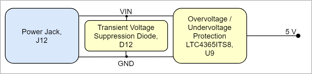 Image Modified Image Modified
|
|
Power Rails
| Scroll Title |
|---|
| anchor | Table_PWR_PR |
|---|
| title | Module power rails.Power Rails |
|---|
|
| Scroll Table Layout |
|---|
| orientation | portrait |
|---|
| sortDirection | ASC |
|---|
| repeatTableHeaders | default |
|---|
| style | |
|---|
| widths | |
|---|
| sortByColumn | 1 |
|---|
| tableStyling | confluence |
|---|
| sortEnabled | false |
|---|
| cellHighlighting | true |
|---|
|
VCC / | Pin | Direction | Notes | Pin | VCC | Direction | Notes |
|---|
| J12 | VIN | 1 | 5 V | In |
| | J3 | 3.3V | 2, 4 | 3.3 V | Out |
| | 5V | 5 | 5 V | Out |
| | J5 | 3.3V | 3 | 3.3 V | Out |
|
|
Bank Voltages
| Scroll Title |
|---|
| anchor | Table_PWR_BV |
|---|
| title | Zynq SoC bank voltages.Intel Cyclone 10 LP Bank Voltages |
|---|
|
| Scroll Table Layout |
|---|
| orientation | portrait |
|---|
| sortDirection | ASC |
|---|
| repeatTableHeaders | default |
|---|
| style | |
|---|
| widths | |
|---|
| sortByColumn | 1 |
|---|
| sortEnabled | false |
|---|
| cellHighlighting | true |
|---|
|
| Schematic Name | | Notes | | Notes |
|---|
| Bank 1...8 | VCCIO1...8 | Bank 1 | VCCIO1 | 3.3V | Bank 2 | VCCIO2 | 3.3V | Bank 3 | VCCIO3 | 3.3V | Bank 4 | VCCIO4 | 3.3V | Bank 5 | VCCIO5 | 3.3V | Bank 6 | VCCIO6 | 3.3V | Bank 7 | VCCIO7 | 3.3V | Bank 8 | VCCIO8 | 3.3V |
|
|
Technical Specifications
Absolute Maximum Ratings
| Scroll Title |
|---|
| anchor | Table_TS_AMR |
|---|
| title | PS absolute maximum ratingsAbsolute Maximum Ratings |
|---|
|
| Scroll Table Layout |
|---|
| orientation | portrait |
|---|
| sortDirection | ASC |
|---|
| repeatTableHeaders | default |
|---|
| style | widths |
|---|
| sortByColumn | 1 |
|---|
| sortEnabled | false |
|---|
| cellHighlighting | true |
|---|
| |
|---|
| widths | |
|---|
| sortByColumn | 1 |
|---|
| sortEnabled | false |
|---|
| cellHighlighting | true |
|---|
|
| Symbols | Description | Min | Max | Unit | Note |
|---|
| VIN | Input Supply Voltage (J12)
| 4.5 | 5.5 | V |
| | AREF | External Reference Voltage for ADC/DAC (J1 - 8) | -0.3 | 3.6 | V | Only for input usage. | | AIN0...5 | Input Voltage for ADC/DAC (J4) | -0.3 | 3.6 | V | Only for input usage. | | AIN6...7 | Input Voltage for ADC/DAC (TP1...2) | -0.3 | 3.6 | V | Only for input usage. | | EXT_RST | External Reset (J3 - 3) | -0.5 | 4.2 | V |
| | D0_RXD, D1_TXD, D2...7 | Arduino Interface (J2) |
| Symbols | Description | Min | Max | Unit | Note |
|---|
VIN | Input supply voltage | -5.0 | 5.0 | V | VCCIO | I/O buffers power supply375VCCINT | Core voltage | Only for input usage. | D8...13, D14_SDA, D15_SCL | Arduino Interface (J1 - 1...6, 9...10) | -0.5 |
18VCCD_PLL | PLL digital power supply | Only for input usage. | | I2C_SCL, I2C_SDA | I2C Interface (J5 - 1...2) | -0. |
518VCCA | Phase-locked loop (PLL) analog power supply | -0.5 | 3.75 | V | V_AN | Analog Input Voltage on ADC/DAC (U2) | -0.3 | 3.6 | V | V_DIG | Digital Input Voltage on ADC/DAC (U2| Only for input usage. | P1_IO1...8, P2_IO1...8, P3_IO1...8, P4_IO1...8, P5_IO1...8, P6_IO1...8, | Pmod Interface (P1...6) | -0. |
336V_REF_IN | | Only for input usage. | | CLK_IN | External FPGA Clock (J19 |
Internal Reference Voltage Voltage on ADC/DAC (U2336VREF_EXExternal Reference Voltage Voltage on ADC/DAC (U2336| 2 | V | Only for input usage. | | T_STG | Storage Temperature | -35 | 85 | °C | See LTC2623WC datasheet |
|
Recommended Operating Conditions
...
| Scroll Title |
|---|
| anchor | Table_TS_ROC |
|---|
| title | Recommended operating conditions.Operating Conditions |
|---|
|
| Scroll Table Layout |
|---|
| orientation | portrait |
|---|
| sortDirection | ASC |
|---|
| repeatTableHeaders | default |
|---|
| style | |
|---|
| widths | |
|---|
| sortByColumn | 1 |
|---|
| sortEnabled | false |
|---|
| cellHighlighting | true |
|---|
|
| Parameter | Min | Max | Units | Reference Document |
|
|---|
| VIN | 4.75 | 5.25 | V |
|
| | AREF | VCCIO1 | 3. | 1353.4653 | V |
|
| | AIN0...5 | 0 | AREF | V | See Cyclone 10 LP datasheet. | | VCCINT | 1.15 | 1.25 | V | See Cyclone 10 LP datasheet. | | VCCD_PLL | 1.15 | 1.25 | V | See Cyclone 10 LP datasheet. | | VCCA | 2.375 | 2.625 | V | See Cyclone 10 LP datasheet. | | V_AN | 0 | 3.3 | V | See AD5592RBCPZ datasheet. | | V_DIG | 0 | 3.3 | V | See AD5592RBCPZ datasheet. | | V_REF_IN | 1 | 3 | V | See AD5592RBCPZ datasheet. |
|
| | AIN6...7 | 0 | AREF | V |
|
| | EXT_RST | -0.5 | 3.6 | V |
|
| | D0_RXD, D1_TXD, D2...7 | -0.5 | 3.6 | V |
|
| D8...13, D14_SDA, D15_SCL | -0.5 | 3.6 | V |
|
| | I2C_SCL, I2C_SDA | -0.3 | 3.3 | V |
|
| P1_IO1...8, P2_IO1...8, P3_IO1...8, P4_IO1...8, P5_IO1...8, P6_IO1...8, | -0.5 | 3.6 | V |
|
| | CLK_IN | -0.5 | 3.6 | V |
|
| | CLK_OUT | -0.5 | 3.6 | V | V_REF_EX | 2.45 | 2.55 | V | See AD5592RBCPZ datasheet. |
|
| | T_OP | 0 | 70 | °C | See SDRAM W9864G6JT datasheet |
|
|
...
| Scroll Title |
|---|
| anchor | Figure_TS_PD |
|---|
| title | Physical Dimension |
|---|
|
| Scroll Ignore |
|---|
| draw.io Diagram |
|---|
| border | false |
|---|
| viewerToolbar | true |
|---|
| |
|---|
| fitWindow | false |
|---|
| diagramDisplayName | |
|---|
| lbox | true |
|---|
| revision | 23 |
|---|
| diagramName | TEI0009_TS_PD |
|---|
| simpleViewer | false |
|---|
| width | |
|---|
| links | auto |
|---|
| tbstyle | hidden |
|---|
| diagramWidth | 640 |
|---|
|
|
| Scroll Only |
|---|
| scroll-pdf | true |
|---|
| scroll-office | true |
|---|
| scroll-chm | true |
|---|
| scroll-docbook | true |
|---|
| scroll-eclipsehelp | true |
|---|
| scroll-epub | true |
|---|
| scroll-html | true |
|---|
| 
|
|
...
| Scroll Title |
|---|
| anchor | Table_VCP_SO |
|---|
| title | Trenz Electronic Shop Overview |
|---|
|
| Scroll Table Layout |
|---|
| orientation | portrait |
|---|
| sortDirection | ASC |
|---|
| repeatTableHeaders | default |
|---|
| style | |
|---|
| widths | |
|---|
| sortByColumn | 1 |
|---|
| sortEnabled | false |
|---|
| cellHighlighting | true |
|---|
|
|
Revision History
Hardware Revision History
...
| Scroll Title |
|---|
| anchor | Table_RH_HRH |
|---|
| title | Hardware Revision History |
|---|
|
| Scroll Table Layout |
|---|
| orientation | portrait |
|---|
| sortDirection | ASC |
|---|
| repeatTableHeaders | default |
|---|
| style | |
|---|
| widths | |
|---|
| sortByColumn | 1 |
|---|
| sortEnabled | false |
|---|
| cellHighlighting | true |
|---|
|
| Date | Revision | Changes | Document Link |
|---|
| 2018-2-19 | 01 | - |
REV01 connector connectorConnect clock - Connector
- Change connection of 12 MHz clock from Bank 1 to Bank
|
1Connect SLA/SDA - SDA/SCL from Bank 3 to Bank
|
3Remove SMA Coaxial straight J19,J20- SMA Coaxial Connector J19, J20 not mounted
- Change connection of CLK_IN/CLK_OUT from Bank 4 to Bank 8
- Remove DIP Switch S1
- Add 5
|
red buttons flash memory memory, 143 MHz to 166 MHz 10bit 10bit 12bit DAC/ADCRemove SMA Coaxial straight J19,J20Remove SMA Coaxial straight J19,J20Remove Tranciever USBRemove DIP switch S2Different Power DependenciesRemove 24MHz Oscillator- 12-Bit ADC/DAC
- Remove USB Transceiver
- Remove 24 MHz Oscillator
- Remove DIP Switch S2
- Changed Power Supply Circuit
- Add 4 Pmod Host Sockets
|
Add 4x Pmod SMD host socket
|
Hardware revision number can be found on the PCB board together with the module model number separated by the dash.
| Scroll Title |
|---|
| anchor | Figure_RV_HRN |
|---|
| title | Board hardware revision number.Hardware Revision Number |
|---|
|
| Scroll Ignore |
|---|
| draw.io Diagram |
|---|
| border | false |
|---|
| viewerToolbar | true |
|---|
| |
|---|
| fitWindow | false |
|---|
| diagramDisplayName | |
|---|
| lbox | true |
|---|
| revision | 2 |
|---|
| diagramName | TEI0009_RV_HRN |
|---|
| simpleViewer | false |
|---|
| width | |
|---|
| links | auto |
|---|
| tbstyle | hidden |
|---|
| diagramWidth | 196 |
|---|
|
|
| Scroll Only |
|---|
|
|
...
| Scroll Title |
|---|
| anchor | Table_RH_DCH |
|---|
| title | Document change history.Change History |
|---|
|
| Scroll Table Layout |
|---|
| orientation | portrait |
|---|
| sortDirection | ASC |
|---|
| repeatTableHeaders | default |
|---|
| style | |
|---|
| widths | |
|---|
| sortByColumn | 1 |
|---|
| sortEnabled | false |
|---|
| cellHighlighting | true |
|---|
|
| Date | Revision | Contributor | Description |
|---|
| Page info |
|---|
| infoType | Modified date |
|---|
| dateFormat | yyyy-MM-dd |
|---|
| type | Flat |
|---|
|
| | Page info |
|---|
| infoType | Current version |
|---|
| prefix | v. |
|---|
| type | Flat |
|---|
| showVersions | false |
|---|
|
| | Page info |
|---|
| infoType | Modified by |
|---|
| type | Flat |
|---|
| showVersions | false |
|---|
|
| - change listinitial release
| -- | all | | Page info |
|---|
| infoType | Modified users |
|---|
| type | Flat |
|---|
| showVersions | false |
|---|
|
| |
|
...