Initial delivery state of programmable devices Delivery State of Programmable Devices on the moduleModule
Scroll Table Layout
orientation
portrait
sortDirection
ASC
repeatTableHeaders
default
style
widths
sortByColumn
1
sortEnabled
false
cellHighlighting
true
Storage device name
Content
Notes
QSPI Flash (U12)
Not programmed
EEPROM (U15)
Programmed
FTDI Configuration
EEPROM (U18, U20)
Not programmed
Except Ethernet MAC
SDRAM (U10)
Not programmed
PSRAM (U3)
Not programmed
Serial Configuration Memory (U5)
Programmed
...
Scroll Title
anchor
Table_OV_BP
title
Boot process.Process
Scroll Table Layout
orientation
portrait
sortDirection
ASC
repeatTableHeaders
default
style
widths
sortByColumn
1
sortEnabled
false
cellHighlighting
true
MODE Signal State
MSEL0
MSEL1
MSEL2
MSEL3
Connected to
Boot Mode
MSEL[0:3]
0
1
0
0
Bank 6
AS (Active Serial)
...
Scroll Title
anchor
Table_OV_RST
title
Reset process.Process
Scroll Table Layout
orientation
portrait
sortDirection
ASC
repeatTableHeaders
default
style
widths
sortByColumn
1
sortEnabled
false
cellHighlighting
true
Signal
Connected to
Note
RESET
S7, Push Button
Connected to nCONFIG.
...
Scroll Title
anchor
Table_SIP_B2B
title
General I/O to Pin Header and Pmod connectors informationConnectors Information
Scroll Table Layout
orientation
portrait
sortDirection
ASC
repeatTableHeaders
default
style
widths
sortByColumn
1
sortEnabled
false
cellHighlighting
true
FPGA Bank
Connector
I/O Signal Count
Voltage Level
Notes
Bank 1
J1 (Pin header)
8 Single ended
3.3 V
J2 (Pin header)
8 Single ended
3.3 V
J4 (Pin header)
6 Single ended
3.3 V
Bank 2
J3 (Pin header)
1 Single ended
3.3 V
P1 (Pmod Host Socket)
8 Single ended
3.3 V
P2 (Pmod Host Socket)
8 Single ended
3.3 V
J11 (VGA Host Socket)
14 Single ended
3.3 V
Bank 6
J5 (Grove Connector)
2 Single ended
3.3 V
Bank 7
P5 (Pmod Host Socket)
8 Single ended
3.3 V
P6 (Pmod Host Socket)
8 Single ended
3.3 V
Bank 8
P3 (Pmod Host Socket)
8 Single ended
3.3 V
P4 (Pmod Host Socket)
8 Single ended
3.3 V
...
Scroll Title
anchor
Table_SIP_SMD
title
Pmod SMD host socket informationHost Socket Information
Scroll Table Layout
orientation
portrait
sortDirection
ASC
repeatTableHeaders
default
style
widths
sortByColumn
1
sortEnabled
false
cellHighlighting
true
Designator
Signals
Connected to
Notes
P1
P1_IO1...8
Bank 2
P2
P2_IO1...8
Bank 2
P3
P3_IO1...8
Bank 8
P4
P4_IO1...8
Bank 8
P5
P5_IO1...8
Bank 7
P6
P6_IO1...8
Bank 7
...
Scroll Title
anchor
Table_SIP_RJ45
title
RJ45 connectors informationConnectors Information
Scroll Table Layout
orientation
portrait
sortDirection
ASC
repeatTableHeaders
default
style
widths
sortByColumn
1
sortEnabled
false
cellHighlighting
true
Pin
Schematic
ETH1 Pin
ETH2 Pin
Notes
TD+
ETH1_TX_P, ETH2_TX_P
U17 - TXP
U19 - TXP
CT
ETH1_CTREF_TCT, ETH2_CTREF_TCT
-
-
TD-
ETH1_TX_N, ETH2_TX_N
U17 - TXM
U19 - TXM
RD+
ETH1_RX_P, ETH2_RX_P
U17 - RXP
U19 - RXP
CT
ETH1_CTREF_RCT, ETH2_CTREF_RCT
-
-
RD-
ETH1_RX_N, ETH2_RX_N
U17 - RXM
U19 - RXM
LED Green
ETH1_LED0, ETH2_LED0
U17 - LED0/NWAYEN
U19 - LED0/NWAYEN
LED Yellow
ETH1_LED1, ETH2_LED1
U17 - LED1/SPEED
U19 - LED1/SPEED
...
Scroll Title
anchor
Table_SIP_VGA
title
VGA host socket informationHost Socket Information
Scroll Table Layout
orientation
portrait
sortDirection
ASC
repeatTableHeaders
default
style
widths
sortByColumn
1
sortEnabled
false
cellHighlighting
true
Schematic
Corresponding Signals
Connected to
Notes
VGA_RED
VGA_R0...3
Bank 2
Red Channel
VGA_GREEN
VGA_G0...3
Bank 2
Green Channel
VGA_BLUE
VGA_B0...3
Bank 2
Blue Channel
VGA_RGB_HSYNC
VGA_HS
Bank 2
Horizontal Sync
VGA_RGB_VSYNC
VGA_VS
Bank 2
Vertical Sync
...
Scroll Title
anchor
Table_OBP_SPI
title
Quad SPI interface Interface MIOs and pinsPins
Scroll Table Layout
orientation
portrait
sortDirection
ASC
repeatTableHeaders
default
style
widths
sortByColumn
1
sortEnabled
false
cellHighlighting
true
Pin
Schematic
Connected to
Notes
CS
F_CS
Bank 7
CLK
F_CLK
Bank 7
IO0...3
F_IO0...3
Bank 7
...
The TEI0009 is integrated with 64 Mbit (8 MByte) Pseudo Static Random Access Memory (PSRAM) using a self-refresh DRAM array organized as 8M words by 8 bits. The device supports a HyperBus interface, Very Low Signal Count (Address, Command and data through 8 DQ pins), Hidden Refresh Operation, and Automotive Temperature Operation. Up to 128 MBit (16 MByte) memory is available on other assembly option.
Part number: IS66WVH8M8BLLIS66WVH8M8
Supply voltage: 3.3 V
Clock Frequency: 100 MHz
Temperature: -40°C to 85°C (optional other ranges are available)
...
Scroll Title
anchor
Table_OBP_7SEG
title
7-Segment LED pinsPins
Scroll Table Layout
orientation
portrait
sortDirection
ASC
repeatTableHeaders
default
style
widths
sortByColumn
1
sortEnabled
false
cellHighlighting
true
Pin
Schematic
Connected to
Notes
A/L1
SEG_CA
Bank 6
B/L2
SEG_CB
Bank 6
C/L3
SEG_CC
Bank 6
D
SEG_CD
Bank 6
E
SEG_CE
Bank 6
F
SEG_CF
Bank 6
G
SEG_CG
Bank 6
DP
SEG_CDP
Bank 6
A1
SEG_AN
Bank 6
A2
SEG_AN4
Bank 6
A3
SEG_AN3
Bank 6
A4
SEG_AN2
Bank 6
L1-L3
SEG_AN1
Bank 6
...
Scroll Title
anchor
Table_OBP_FTDI
title
FTDI chip interfaces Chip Interfaces and pinsPins
Scroll Table Layout
orientation
portrait
sortDirection
ASC
repeatTableHeaders
default
style
widths
sortByColumn
1
sortEnabled
false
cellHighlighting
true
FTDI Chip Pin
Signal Schematic Name
Connected to
Notes
ADBUS0
TCK
Bank 1
JTAG interface
ADBUS1
TDI
Bank 1
ADBUS2
TDO
Bank 1
ADBUS3
TMS
Bank 1
BDBUS0...7
BDBUS0...7
Bank 6
BCBUS0...7
BCBUS0...7
Bank 6
EECS
EECS
EEPROM, U15
EECLK
EECLK
EEPROM, U15
EEDATA
EEDATA
EEPROM, U15
OSCI
CK12M
12 MHz Oscillator, U16
DM
D_N
Micro USB 2.0, J10
DP
D_P
Micro USB 2.0, J10
...
Scroll Title
anchor
Table_OBP_ETH
title
Ethernet PHY connections Connections and pinsPins
Scroll Table Layout
orientation
portrait
sortDirection
ASC
repeatTableHeaders
default
style
widths
sortByColumn
1
sortEnabled
false
cellHighlighting
true
Ethernet PHY Pin
Signal Schematic Names (ETH1/ETH2)
ETH 1
ETH 2
Note
TXD0...3
ETH1_TXD0...3, ETH2_TXD0...3
Bank 5
Bank 5
TXC
ETH1_TXC, ETH2_TXC
Bank 5
Bank 5
TXEN
ETH1_TXEN, ETH2_TXEN
Bank 5
Bank 5
RXD0...3
ETH1_RXD0...3, ETH2_RXD0...3
Bank 5
Bank 5
RXC/B-CAST_OFF
ETH1_RXC, ETH2_RXC
Bank 5
Bank 5
RXER/ISO
ETH1_RXER, ETH2_RXER
Bank 5
Bank 5
INTRP/nNAND_Tree
ETH1_INTRP, ETH2_INTRP
Bank 5
Bank 5
XI
ETH1_CLKIN, ETH2_CLKIN
Oscillator, U22
Oscillator, U22
MDC
ETH1_MDC, ETH2_MDC
Bank 5
Bank 5
MDIO
ETH1_MDIO, ETH2_MDIO
Bank 5
Bank 5
COL/CONFIG0
ETH1_COL, ETH2_COL
Bank 5
Bank 5
CRS/CONFIG1
ETH1_CRS, ETH2_CRS
Bank 5
Bank 5
RXDV/CONFIG2
ETH1_RXDV, ETH2_RXDV
Bank 5
Bank 5
LED0/NWAYEN
ETH1_LED0, ETH2_LED0
RJ45 - Green LED, J8
RJ45 - Green LED, J9
LED1/SPEED
ETH1_LED1, ETH2_LED1
RJ45 - Yellow LED, J8
RJ45 - Yellow LED, J9
nRST
ETH1_RST, ETH2_RST
Bank 5
Bank 5
RXM
ETH1_RX_N, ETH2_RX_N
RJ45, J8
RJ45, J9
RXP
ETH1_RX_P, ETH2_RX_P
RJ45, J8
RJ45, J9
TXM
ETH1_TX_N, ETH2_TX_N
RJ45, J8
RJ45, J9
TXP
ETH1_TX_P, ETH2_TX_P
RJ45, J8
RJ45, J9
...
Scroll Title
anchor
Table_OBP_EEP
title
FTDI and EEPROM pin connectionsPin Connections
Scroll Table Layout
orientation
portrait
sortDirection
ASC
repeatTableHeaders
default
style
widths
sortByColumn
1
sortEnabled
false
cellHighlighting
true
Designator
EEPROM Pin
Signal Schematic Names
Connected to
Notes
U15
CS
EECS
FTDI, U14
CLK
EECLK
FTDI, U14
DIN/DOUT
EEDATA
FTDI, U14
...
Scroll Title
anchor
Table_OBP_EEP
title
I2C EEPROM interface Interface MIOs and pinsPins
Scroll Table Layout
orientation
portrait
sortDirection
ASC
repeatTableHeaders
default
style
widths
sortByColumn
1
sortEnabled
false
cellHighlighting
true
Designator
Pin
Schematic
Connected to
Grove Header
Notes
U18, U20
SCL
I2C_SCL
Bank 6
J5
SDA
I2C_SDA
Bank 6
J5
...
Scroll Title
anchor
Table_OBP_I2C_EEPROM
title
I2C address Address for EEPROM
Scroll Table Layout
orientation
portrait
sortDirection
ASC
repeatTableHeaders
default
style
widths
sortByColumn
1
sortEnabled
false
cellHighlighting
true
I2C Address
Designator
Notes
0x50
U18
0x51
U20
...
Scroll Title
anchor
Table_OBP_A2D
title
ADC/DAC interface Interface and pinsPins
Scroll Table Layout
orientation
portrait
sortDirection
ASC
repeatTableHeaders
default
style
widths
sortByColumn
1
sortEnabled
false
cellHighlighting
true
Pins
Schematic
Connected to
Notes
nRESET
ADDA_RSTN
Bank 2, U1
nSYNC
ADDA_SYNC
Bank 2, U1
SCLK
MCLK
Bank 2, U1
SDI
MOSI
Bank 2, U1
SDO
MISO
Bank 2, U1
VREF
AREF
Pin Header, J1
External reference is 1 V to 3.3 V. Internal reference is 2.5 V.
IO0...5
AIN0...5
Bank 1, U1
Pin Header, J4
IO6
AIN6
Testpoint, TP1
IO7
AIN7
Testpoint, TP2
...
Scroll Title
anchor
Figure_PWR_PD
title
Power Distribution
Scroll Ignore
draw.io Diagram
border
false
viewerToolbar
true
fitWindow
false
diagramDisplayName
lbox
true
revision
911
diagramName
TEI0009_PWR_PD
simpleViewer
false
width
links
auto
tbstyle
hidden
diagramWidth
639540
Scroll Only
Power-On Sequence
...
Scroll Title
anchor
Figure_PWR_PS
title
Power Sequency
Scroll Ignore
draw.io Diagram
border
false
viewerToolbar
true
fitWindow
false
diagramDisplayName
lbox
true
revision
710
diagramName
TEI0009_PWR_PS
simpleViewer
false
width
links
auto
tbstyle
hidden
diagramWidth
518538
Scroll Only
Voltage Protection Circuit
...
Scroll Title
anchor
Figure_PWR_VMC
title
Voltage Protection Circuit
Scroll Ignore
draw.io Diagram
border
false
viewerToolbar
true
fitWindow
false
diagramDisplayName
lbox
true
revision
35
diagramName
TEI0009_PWR_VM
simpleViewer
false
width
links
auto
tbstyle
hidden
diagramWidth
490509
Scroll Only
Image Modified
Power Rails
Scroll Title
anchor
Table_PWR_PR
title
Module Power Rails
Scroll Table Layout
orientation
portrait
sortDirection
ASC
repeatTableHeaders
default
style
widths
sortByColumn
1
tableStyling
confluence
sortEnabled
false
cellHighlighting
true
Connector Designator
VCCIO Schematic Name
Pin
VCC
Direction
Notes
J12
VIN
1
5 V
In
J3
3.3V
2, 4
3.3 V
Out
5V
5
5 V
Out
J5
3.3V
3
3.3 V
Out
Bank Voltages
Scroll Title
anchor
Table_PWR_BV
title
Intel Cyclone 10 LP bank voltagesBank Voltages
Scroll Table Layout
orientation
portrait
sortDirection
ASC
repeatTableHeaders
default
style
widths
sortByColumn
1
sortEnabled
false
cellHighlighting
true
Bank
Schematic Name
Voltage
Notes
Bank 1...8
VCCIO1...8
3.3V
...
Scroll Title
anchor
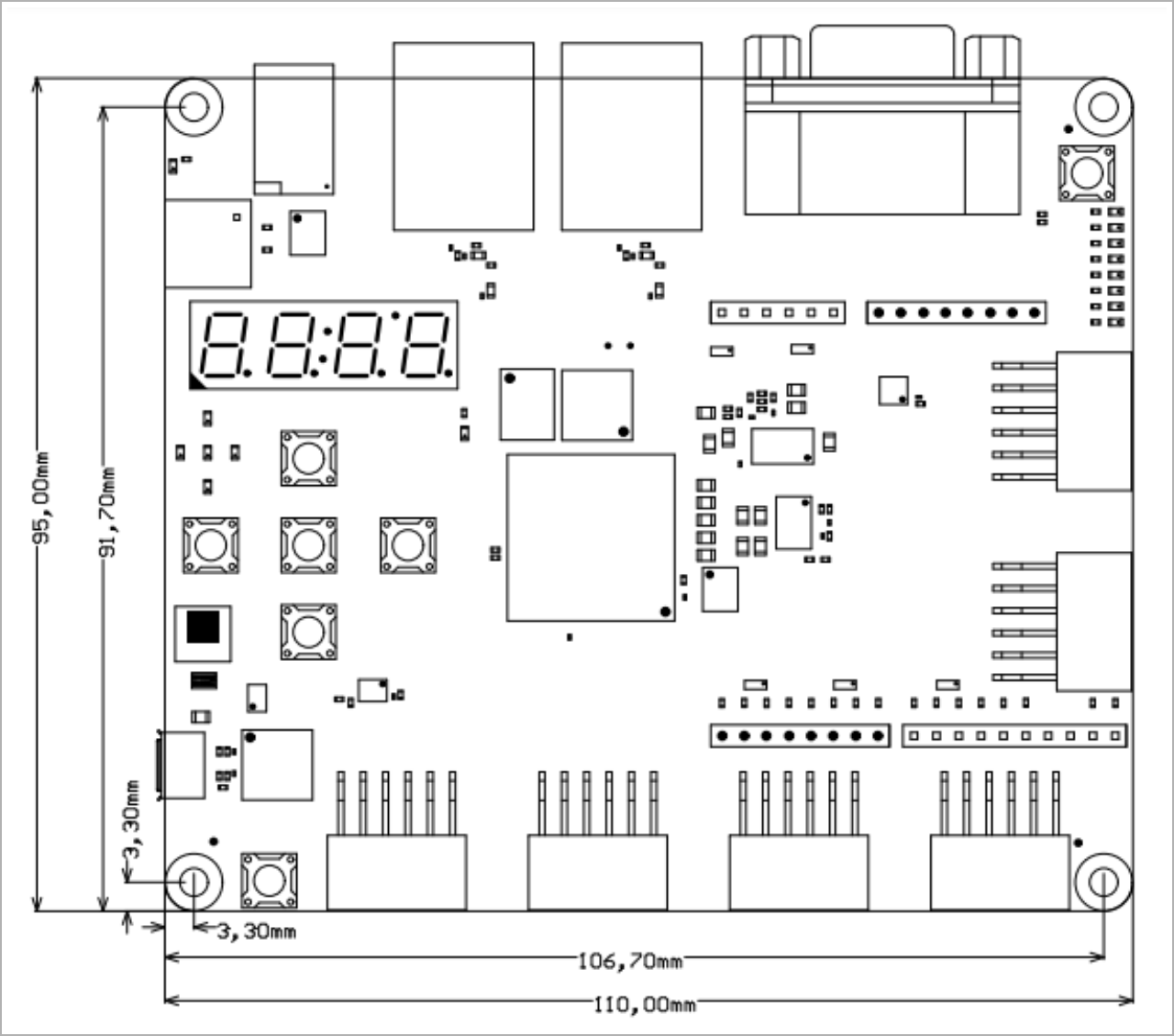
Figure_TS_PD
title
Physical Dimension
Scroll Ignore
draw.io Diagram
border
false
viewerToolbar
true
fitWindow
false
diagramDisplayName
lbox
true
revision
23
diagramName
TEI0009_TS_PD
simpleViewer
false
width
links
auto
tbstyle
hidden
diagramWidth
640
Scroll Only
scroll-pdf
true
scroll-office
true
scroll-chm
true
scroll-docbook
true
scroll-eclipsehelp
true
scroll-epub
true
scroll-html
true
...
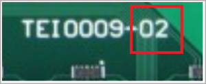
Scroll Title
anchor
Figure_RV_HRN
title
Board hardware revision number.Hardware Revision Number