...
| Page properties |
|---|
|
Note for Download Link of the Scroll ignore macro: |
| Scroll pdf ignore |
|---|
Table of Contents |
Overview
The Cyclone10 Cyclone 10 LP Reference Kit is the world's first development board with a 55kLE 55 kLE (Logic Elements) Intel Cyclone 10 LP and a variety of interfaces for numerous applications. The board is comprehensively tested and ready for use with end products and can also be ordered in customer-specific variants according to your requirements.
...
Key Features
| Page properties |
|---|
|
Note:
'Key Features' description: Important components and connector or other Features of the module
→ please sort and indicate assembly options |
- Intel Cyclone 10 LP FPGA 10CL055YU484C8G, 55 kLE in 484-pin[10CL055YU484C8G]
- Package: UBGA-484
- Speed Grade: 8 (Slowest)
- Temperature: 0 °C to 85° C
- Package compatible device 10CL016, 10CL040, 10CL055, 10CL080 as assembly variant on request is possible
- 16 MBit (2 MByte) Flash Memory 16 MBit flash memory (optional up to 32 MBit possibleMBit (4 MByte))
- Integrated USB-JTAG Programmer 2
- Pin Header Connectors
- 256 64 MBit (8 MByte) SDRAM (optional up to 512 MBit possible(64 MByte)) SDRAM128
- 64 MBit (optional up to 512 MBit possible8 MByte) User Quad-SPI Flash memoryMemory (optional up to 128 MBit (16 MByte))
- 64 MBit (8 MByte) HyperRAM (Pseudo SRAM) (optional up to 128 MBit possible(16 MByte))
- 2 x 2x MAC address Address EEPROM
- 2 x 2x Fast Ethernet PHY (10/100 Mbps)
- 8-channelChannel, 12-bitBit, configurable ADC/DAC with on-chip reference
- D-Sub Connector
- 2x RJ45 Connector
- LEDs:
- Status LEDs, Power LED
- 13 x 13x User LEDs
- 1 x 7-segment display
- 2 x reset buttons
- Segment Display
- Push Buttons:
- 2x Reset Push Buttons
- 5x User Push Buttons
- I/O: 70 GPIO
- 5 V Power Supply
- Dimension: 95 mm x 110 mm
- Others:
- Reverse Supply Protection
- Undervoltage/Overvoltage Protection5 x user buttons
Block Diagram
| Page properties |
|---|
|
add drawIO object here.
|
...
| Scroll Title |
|---|
| anchor | Figure_OV_BD |
|---|
| title | TEI0009 block diagramBlock Diagram |
|---|
|
| Scroll Ignore |
|---|
| draw.io Diagram |
|---|
| border | false |
|---|
| viewerToolbar | true |
|---|
| |
|---|
| fitWindow | false |
|---|
| diagramDisplayName | |
|---|
| lbox | true |
|---|
| revision | 117 |
|---|
| diagramName | TEI0009_OV_BD |
|---|
| simpleViewer | false |
|---|
| width | |
|---|
| links | auto |
|---|
| tbstyle | hidden |
|---|
| diagramWidth | 641640 |
|---|
|
|
| Scroll Only |
|---|

|
|
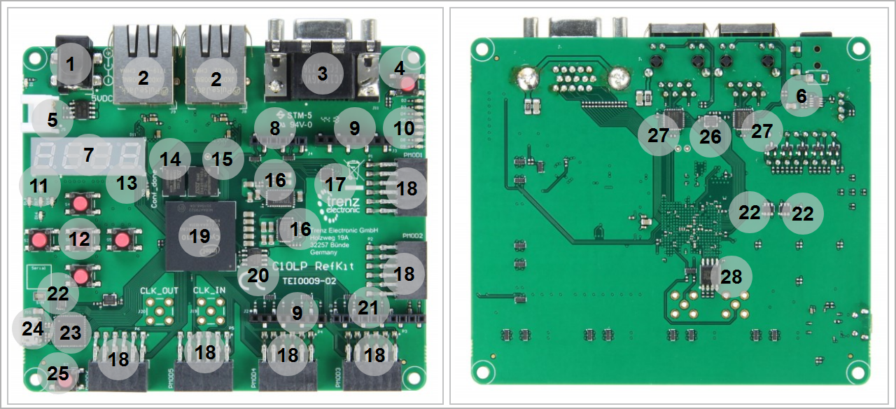
Main Components
| Page properties |
|---|
|
Notes : - Picture of the PCB (top and bottom side) with labels of important components
- Add List below
|
...
| Scroll Title |
|---|
| anchor | Figure_OV_BD |
|---|
| title | TExxxx main componentsTEI0009 Main Components |
|---|
|
| Scroll Ignore |
|---|
| draw.io Diagram |
|---|
| border | false |
|---|
| viewerToolbar | true |
|---|
| |
|---|
| fitWindow | false |
|---|
| diagramDisplayName | |
|---|
| lbox | true |
|---|
| revision | 27 |
|---|
| diagramName | TEI0009_OV_MC |
|---|
| simpleViewer | false |
|---|
| width | |
|---|
| links | auto |
|---|
| tbstyle | hidden |
|---|
| diagramWidth | 640 |
|---|
|
|
| Scroll Only |
|---|
|
|
- Power Jack, J12
- RJ45 Socket, J8
- ...
- ...
- ...
Initial Delivery State
| Page properties |
|---|
|
Notes : Only components like EEPROM, QSPI flash and DDR3 can be initialized by default at manufacture. If there is no components which might have initial data ( possible on carrier) you must keep the table empty |
...
| anchor | Table_OV_IDS |
|---|
| title | Initial delivery state of programmable devices on the module |
|---|
- 9
- D-Sub Connector, J11
- Push Button (Reset), S7
- Grove Connector, J5
- Undervoltage/Overvoltage Protector, U9
- 7-Segment LED, D11
- 1x6 Pin Header, J4
- 1x8 Pin Header, J2...3
- 8x User LEDs (Red), D2...9
- 5x User LEDs (Red), D13...17
- 5x User Push Buttons, S1 - S3...6
- Red LED (CONF_DONE), D10
- PSRAM Memory, U3
- SDRAM Memory, U10
- Voltage Regulator, U4 - U7
- AD/DA Converter, U2
- 6x Pmod Host Socket, P1...6
- Intel Cyclone 10 LP, U1
- Serial Configuration Memory, U5
- 1x10 Pin Header, J1
- EEPROM, U15 - U18 - U20
- FTDI USB 2 to JTAG/UART Converter, U14
- Micro USB 2.0, J10
- Push Button (RST_GPIO), S2
- Oscillator, U22
- Ethernet PHY, U17 - U19
- QSPI Flash Memory, U12
Initial Delivery State
| Page properties |
|---|
|
Notes : Only components like EEPROM, QSPI flash and DDR3 can be initialized by default at manufacture. If there is no components which might have initial data ( possible on carrier) you must keep the table empty |
...
Storage device name
...
Content
...
Notes
...
Quad SPI Flash
...
Configuration Signals
| Page properties |
|---|
|
| Overview of Boot Mode, Reset, Enables. |
| Scroll Title |
|---|
| anchor | Table_OV_BPIDS |
|---|
| title | Boot process.Initial Delivery State of Programmable Devices on the Module |
|---|
|
| Scroll Table Layout |
|---|
| orientation | portrait |
|---|
| sortDirection | ASC |
|---|
| repeatTableHeaders | default |
|---|
| style | |
|---|
| widths | |
|---|
| sortByColumn | 1 |
|---|
| sortEnabled | false |
|---|
| cellHighlighting | true |
|---|
|
|
MODE Signal State | Boot Mode |
|---|
| Scroll Title |
|---|
| anchor | Table_OV_RST |
|---|
| title | Reset process. |
|---|
|
| Scroll Table Layout |
|---|
| orientation | portrait |
|---|
| sortDirection | ASC |
|---|
| repeatTableHeaders | default |
|---|
style | widths | | sortByColumn | 1 |
|---|
| sortEnabled | false |
|---|
| cellHighlighting | true |
|---|
Signal | B2B | I/O | Note |
|---|
Signals, Interfaces and Pins
| Page properties |
|---|
|
Notes : - For carrier or stand-alone boards use subsection for every connector type (add designator on description, not on the subsection title), for example:
- For modules which needs carrier use only classes and refer to B2B connector if more than one is used, for example
|
Board to Board (B2B) I/Os
FPGA bank number and number of I/O signals connected to the B2B connector:
Storage device name | Content | Notes |
|---|
QSPI Flash (U12) | Not programmed |
| | EEPROM (U15) | Programmed | FTDI Configuration | | EEPROM (U18, U20) | Not programmed | Except Ethernet MAC | | SDRAM (U10) | Not programmed |
| | PSRAM (U3) | Not programmed |
| | Serial Configuration Memory (U5) | Programmed |
|
|
Configuration Signals
| Page properties |
|---|
|
- Overview of Boot Mode, Reset, Enables.
|
Configuration mode has been set to AS (Active Serial) configuration.
| Scroll Title |
|---|
| anchor | Table_OV_BP |
|---|
| title | Boot Process |
|---|
|
| Scroll Table Layout |
|---|
| orientation | portrait |
|---|
| sortDirection | ASC |
|---|
| repeatTableHeaders | default |
|---|
| style | |
|---|
| widths | |
|---|
| sortByColumn | 1 |
|---|
| sortEnabled | false |
|---|
| cellHighlighting | true |
|---|
|
MODE Signal State | MSEL0 | MSEL1 | MSEL2 | MSEL3 | Connected to | Boot Mode |
|---|
MSEL[0:3] | 0 | 1 | 0 | 0 | Bank 6 | AS (Active Serial) |
|
| Scroll Title |
|---|
| anchor | Table_OV_RST |
|---|
| title | Reset Process |
|---|
|
| Scroll Title |
|---|
| anchor | Table_SIP_B2B |
|---|
| title | General PL I/O to B2B connectors information |
|---|
|
| Scroll Table Layout |
|---|
| orientation | portrait |
|---|
| sortDirection | ASC |
|---|
| repeatTableHeaders | default |
|---|
| style | |
|---|
| widths | |
|---|
| sortByColumn | 1 |
|---|
| sortEnabled | false |
|---|
| cellHighlighting | true |
|---|
|
|
| FPGA Bank | B2B Connector | I/O Signal Count | Voltage Level | Notes |
|---|
...
JTAG access to the TExxxx SoM through B2B connector JMX.
...
| anchor | Table_SIP_JTG |
|---|
| title | JTAG pins connection |
|---|
...
JTAG Signal
...
B2B Connector
...
MIO Pins
...
you must fill the table below with group of MIOs which are connected to a specific components or peripherals, you do not have to specify pins in B2B, Just mention which B2B is connected to MIOs. The rest is clear in the Schematic.
Example:
Signal | Connected to | Note |
|---|
RESET | S7, Push Button | Connected to nCONFIG. |
|
Signals, Interfaces and Pins
| Page properties |
|---|
|
Notes : - For carrier or stand-alone boards use subsection for every connector type (add designator on description, not on the subsection title), for example:
- For modules which needs carrier use only classes and refer to B2B connector if more than one is used, for example
|
I/Os on Pin Headers and Connectors
FPGA bank number and number of I/O signals connected to the connectors:
| Scroll Title |
|---|
| anchor | Table_SIP_B2B |
|---|
| title | General I/O to Pin Header and Pmod Connectors Information |
|---|
|
| Scroll Table Layout |
|---|
| orientation | portrait |
|---|
| sortDirection | ASC |
|---|
| repeatTableHeaders | default |
|---|
| style | |
|---|
| widths | |
|---|
| sortByColumn | 1 |
|---|
| sortEnabled | false |
|---|
| cellHighlighting | true |
|---|
|
| FPGA Bank | Connector | I/O Signal Count | Voltage Level | Notes |
|---|
| Bank 1 | J1 (Pin header) | 8 Single ended | 3.3 V |
| | J2 (Pin header) | 8 Single ended | 3.3 V |
| | J4 (Pin header) | 6 Single ended | 3.3 V |
| | Bank 2 | J3 (Pin header) | 1 Single ended | 3.3 V |
| | P1 (Pmod Host Socket) | 8 Single ended | 3.3 V |
| | P2 (Pmod Host Socket) | 8 Single ended | 3.3 V |
| | J11 (VGA Host Socket) | 14 Single ended | 3.3 V |
| | Bank 6 | J5 (Grove Connector) | 2 Single ended | 3.3 V |
| | Bank 7 | P5 (Pmod Host Socket) | 8 Single ended | 3.3 V |
| | P6 (Pmod Host Socket) | 8 Single ended | 3.3 V |
| | Bank 8 | P3 (Pmod Host Socket) | 8 Single ended | 3.3 V |
| | P4 (Pmod Host Socket) | 8 Single ended | 3.3 V |
|
|
Pmod Host Socket
TEI0009 has 6 Pmod 2x6 host sockets which are connected to Cyclon 10 LP (U1).
...
SPI_CS , SPI_DQ0... SPI_DQ3
SPI_SCK
...
| anchor | Table_OBP_MIOs |
|---|
| title | MIOs pins |
|---|
...
| Page properties |
|---|
|
Notes : - add subsection for every component which is important for design, for example:
- Two 100 Mbit Ethernet Transciever PHY
- USB PHY
- Programmable Clock Generator
- Oscillators
- eMMCs
- RTC
- FTDI
- ...
- DIP-Switches
- Buttons
- LEDs
|
...
Notes :
...
| Scroll Title |
|---|
| anchor | Table_SIP_OBPSMD |
|---|
| title | On board peripheralsPmod SMD Host Socket Information |
|---|
|
| Scroll Table Layout |
|---|
| orientation | portrait |
|---|
| sortDirection | ASC |
|---|
| repeatTableHeaders | default |
|---|
| style | |
|---|
| widths | |
|---|
| sortByColumn | 1 |
|---|
| sortEnabled | false |
|---|
| cellHighlighting | true |
|---|
|
Chip/Interface |
Quad SPI Flash Memory
| Page properties |
|---|
|
Notes : Minimum and Maximum density of quad SPI flash must be mentioned for other assembly options. |
...
| anchor | Table_OBP_SPI |
|---|
| title | Quad SPI interface MIOs and pins |
|---|
| Signals | Connected to | Notes |
|---|
| P1 | P1_IO1...8 | Bank 2 |
| | P2 | P2_IO1...8 | Bank 2 |
| | P3 | P3_IO1...8 | Bank 8 |
| | P4 | P4_IO1...8 | Bank 8 |
| | P5 | P5_IO1...8 | Bank 7 |
| | P6 | P6_IO1...8 | Bank 7 |
|
|
TEI0009 has 5 pin headers. The pin headers J1...4 are usable for Arduino modules, too.
...
| orientation | portrait |
|---|
| sortDirection | ASC |
|---|
| repeatTableHeaders | default |
|---|
| style | |
|---|
| widths | |
|---|
| sortByColumn | 1 |
|---|
| sortEnabled | false |
|---|
| cellHighlighting | true |
|---|
|
...
...
| Scroll Title |
|---|
| anchor | Table_OBPSIP_RTCJ1 |
|---|
| title | I2C interface MIOs and pins |
|---|
| | Scroll Table Layout |
|---|
| orientation | portrait |
|---|
| sortDirection | ASC |
|---|
| repeatTableHeaders | default |
|---|
style | widths | | sortByColumn | 1 |
|---|
| sortEnabled | false |
|---|
| cellHighlighting | true |
|---|
| MIO Pin | Schematic | U? Pin | Notes |
|---|
|
| Pin Header J1 | Signals | Connected to | Notes |
|---|
| J1 - 1...6 | D8...13 | Bank 1 |
| | J1 - 7 | GND |
|
| | J1 - 8 | AREF | ADC/DAC |
| | J1 - 9 | D14_SDA | Bank 1 |
| | J1 - 10 | D14_SCL | Bank 1 |
|
|
| Scroll Title |
|---|
| anchor | Table_OBPSIP_I2C_RTCJ2 |
|---|
| title | I2C Address for RTCPin Header J2 |
|---|
|
| Scroll Table Layout |
|---|
| orientation | portrait |
|---|
| sortDirection | ASC |
|---|
| repeatTableHeaders | default |
|---|
| style | |
|---|
| widths | |
|---|
| sortByColumn | 1 |
|---|
| sortEnabled | false |
|---|
| cellHighlighting | true |
|---|
|
MIO I2C AddressDesignator |
...
|
|---|
| J2 - 1 | D0_RXD | Bank 1 |
| | J2 - 2 | D1_TXD | Bank 1 |
| | J2 - 3...8 | D2...4 | Bank 1 |
|
|
| Scroll Title |
|---|
| anchor | Table_OBPSIP_EEPJ3 |
|---|
| title | I2C EEPROM interface MIOs and pinsPin Header J3 |
|---|
|
| Scroll Table Layout |
|---|
| orientation | portrait |
|---|
| sortDirection | ASC |
|---|
| repeatTableHeaders | default |
|---|
| style | |
|---|
| widths | |
|---|
| sortByColumn | 1 |
|---|
| sortEnabled | false |
|---|
| cellHighlighting | true |
|---|
|
MIO | Schematic | U?? Pin| Signals | Connected to | Notes |
|---|
|
scroll |
title |
| anchor | Table_OBP_I2C_EEPROM |
|---|
| title | I2C address for EEPROM |
|---|
|
| Scroll Table Layout |
|---|
| orientation | portrait |
|---|
| sortDirection | ASC |
|---|
| repeatTableHeaders | default |
|---|
style | widths | | sortByColumn | 1 |
|---|
| sortEnabled | false |
|---|
| cellHighlighting | true |
|---|
| MIO Pin | I2C Address | Designator | Notes |
|---|
LEDs
| NC | - |
| | J3 - 2 | 3.3V | 3.3 V |
| | J3 - 3 | EXT_RST | Bank 2 | Pulled-up to 3.3 V | | J3 - 4 | 3.3V | 3.3 V |
| | J3 - 5 | 5V | 5 V |
| | J3 - 6...7 | GND | GND |
| | J2 - 8 | NC | - |
|
|
| Scroll Title |
|---|
| anchor | Table_SIP_J4 |
|---|
| title | Pin Header J4 |
|---|
|
| Scroll Title |
|---|
| anchor | Table_OBP_LED |
|---|
| title | On-board LEDs |
|---|
|
| Scroll Table Layout |
|---|
| orientation | portrait |
|---|
| sortDirection | ASC |
|---|
| repeatTableHeaders | default |
|---|
| style | |
|---|
| widths | |
|---|
| sortByColumn | 1 |
|---|
| sortEnabled | false |
|---|
| cellHighlighting | true |
|---|
|
SchematicColor to| Active Level | Note | |
DDR3 SDRAM
| Page properties |
|---|
|
Notes : Minimum and Maximum density of DDR3 SDRAM must be mentioned for other assembly options. (pay attention to supported address length for DDR3) |
The TE???? SoM has ??? GByte volatile DDR3 SDRAM IC for storing user application code and data.
- Part number:
- Supply voltage:
- Speed:
- NOR Flash
- Temperature:
Ethernet
...
| anchor | Table_OBP_ETH |
|---|
| title | Ethernet PHY to Zynq SoC connections |
|---|
| to | Notes |
|---|
| J4 - 1...6 | AIN0...5 | FPGA Bank 1 and ADC/DAC |
|
|
| Scroll Title |
|---|
| anchor | Table_SIP_J5 |
|---|
| title | Pin Header J5 |
|---|
|
| Scroll Table Layout |
|---|
| orientation | portrait |
|---|
| sortDirection | ASC |
|---|
| repeatTableHeaders | default |
|---|
| style | |
|---|
| widths | |
|---|
| sortByColumn | 1 |
|---|
| sortEnabled | false |
|---|
| cellHighlighting | true |
|---|
|
| Pin Header J5 | Signals | Connected to | Notes |
|---|
| J5 - 1 | I2C_SCL | FPGA Bank 6 and EEPROM (U18, U20) | Pulled-up to 3.3V. | | J5 - 2 | I2C_SDA | FPGA Bank 6 and EEPROM (U18, U20) | Pulled-up to 3.3V. | | J5 - 3 | 3.3V | 3.3 V |
| | J5 - 4 | GND | GND |
|
|
Micro USB 2.0 Connector
FTDI FT2232 (U14) can be accessed through micro USB 2.0 B connector (J10) for JTAG (channel A). Channel B is connected to the FPGA and can be used for UART or other standards.
RJ45 Connectors
TEI0009 is equipped with two RJ45 connectors and two Ethernet PHYs. RJ45 connectors J8 and J9 are connected to Ethernet PHYs U17 and U19 respectively.
| Scroll Title |
|---|
| anchor | Table_SIP_RJ45 |
|---|
| title | RJ45 Connectors Information |
|---|
|
...
CAN Transceiver
| Scroll Title |
|---|
| anchor | Table_OBP_CAN |
|---|
| title | CAN Tranciever interface MIOs |
|---|
|
| Scroll Table Layout |
|---|
| orientation | portrait |
|---|
| sortDirection | ASC |
|---|
| repeatTableHeaders | default |
|---|
| style | |
|---|
| widths | |
|---|
| sortByColumn | 1 |
|---|
| sortEnabled | false |
|---|
| cellHighlighting | true |
|---|
|
BankU?? | D-Tx | Driver Input | R-Rx | Reciever Output | |
...
| anchor | Table_OBP_CLK |
|---|
| title | Osillators |
|---|
...
Power and Power-On Sequence
...
In 'Power and Power-on Sequence' section there are three important digrams which must be drawn:
- Power on-sequence
- Power distribution
- Voltage monitoring circuit
| Note |
|---|
For more information regarding how to draw diagram, Please refer to "Diagram Drawing Guidline" . |
| TD+ | ETH1_TX_P, ETH2_TX_P | U17 - TXP | U19 - TXP |
| | CT | ETH1_CTREF_TCT, ETH2_CTREF_TCT | - | - |
| | TD- | ETH1_TX_N, ETH2_TX_N | U17 - TXM | U19 - TXM |
| | RD+ | ETH1_RX_P, ETH2_RX_P | U17 - RXP | U19 - RXP |
| | CT | ETH1_CTREF_RCT, ETH2_CTREF_RCT | - | - |
| | RD- | ETH1_RX_N, ETH2_RX_N | U17 - RXM | U19 - RXM |
| | LED Green | ETH1_LED0, ETH2_LED0 | U17 - LED0/NWAYEN | U19 - LED0/NWAYEN |
| | LED Yellow | ETH1_LED1, ETH2_LED1 | U17 - LED1/SPEED | U19 - LED1/SPEED |
|
|
D-Sub Connector
TEI0009 is equipped with a D-Sub connector which provides interface to Cyclone 10 LP through Bank 2.
Power Supply
Power supply with minimum current capability of xx A for system startup is recommended.
Power Consumption
| Scroll Title |
|---|
| anchor | Table_PWRSIP_PCVGA |
|---|
| title | Power ConsumptionVGA Host Socket Information |
|---|
|
| Scroll Table Layout |
|---|
| orientation | portrait |
|---|
| sortDirection | ASC |
|---|
| repeatTableHeaders | default |
|---|
| style | |
|---|
| widths | |
|---|
| sortByColumn | 1 |
|---|
| sortEnabled | false |
|---|
| cellHighlighting | true |
|---|
|
|
| Power Input Pin | Typical Current |
|---|
| VIN | TBD* |
* TBD - To Be Determined
Power Distribution Dependencies
...
| anchor | Figure_PWR_PD |
|---|
| title | Power Distribution |
|---|
| Schematic | Corresponding Signals | Connected to | Notes |
|---|
| VGA_RED | VGA_R0...3 | Bank 2 | Red Channel | | VGA_GREEN | VGA_G0...3 | Bank 2 | Green Channel | | VGA_BLUE | VGA_B0...3 | Bank 2 | Blue Channel | | VGA_RGB_HSYNC | VGA_HS | Bank 2 | Horizontal Sync | | VGA_RGB_VSYNC | VGA_VS | Bank 2 | Vertical Sync |
|
On-board Peripherals
| Page properties |
|---|
|
Notes : - add subsection for every component which is important for design, for example:
- Two 100 Mbit Ethernet Transciever PHY
- USB PHY
- Programmable Clock Generator
- Oscillators
- eMMCs
- RTC
- FTDI
- ...
- DIP-Switches
- Buttons
- LEDs
|
| Page properties |
|---|
|
Notes : In the on-board peripheral table "chip/Interface" must be linked to the corresponding chapter or subsection |
...
| Scroll Only |
|---|
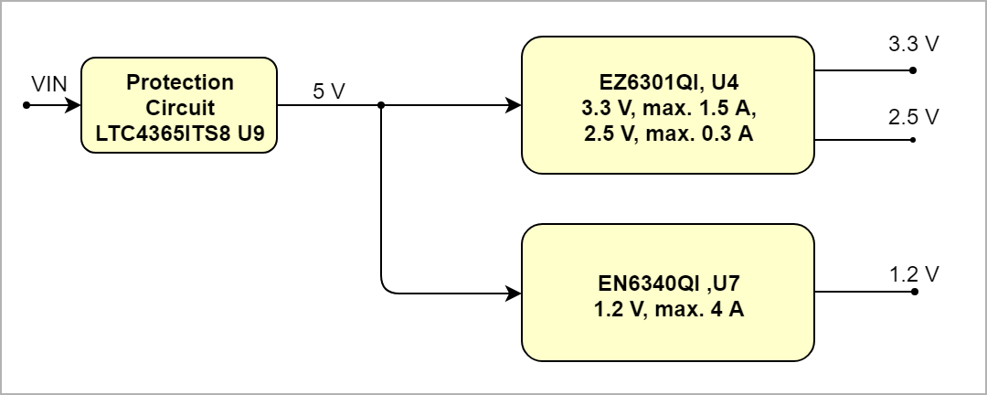 Image Removed Image Removed
|
...
| Scroll Title |
|---|
| anchor | FigureTable_PWR_PSOBP |
|---|
| title | Power SequencyOn-board Peripherals |
|---|
|
| ignoredrawioborderfalseviewerToolbartruefitWindowfalsediagramDisplayNamelboxtruerevision1 |
| diagramName | TEI0009_PWR_PS |
|---|
| simpleViewer | false |
|---|
width | | links | auto |
|---|
| tbstyle | hidden |
|---|
| diagramWidth | 641 |
|---|
| Scroll Only |
|---|
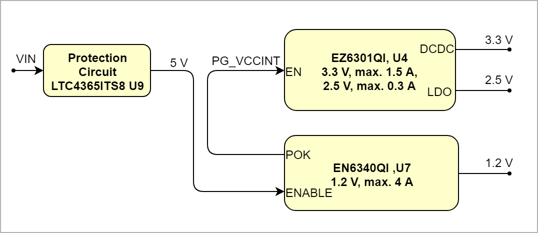 Image Removed Image Removed
|
Voltage Monitor Circuit
...
| anchor | Figure_PWR_VMC |
|---|
| title | Voltage Monitor Circuit |
|---|
| Scroll Ignore |
|---|
Create DrawIO object here: Attention if you copy from other page, objects are only linked. |
| Scroll Only |
|---|
image link to the generate DrawIO PNG file of this page. This is a workaround until scroll pdf export bug is fixed |
QSPI Flash Memory
| Page properties |
|---|
|
Notes : Minimum and Maximum density of quad SPI flash must be mentioned for other assembly options. |
There is a 64 MBit (8 MByte) QSPI Flash memory (U12) provided by Integrated Silicon Solution Inc. which can be used to store data or configuration. Up to 128 MBit (16 MByte) memory is available on other assembly option.
| Scroll Title |
|---|
| anchor | Table_OBP_SPI |
|---|
| title | Quad SPI Interface MIOs and Pins |
|---|
|
Power Rails
...
| anchor | Table_PWR_PR |
|---|
| title | Module power rails. |
|---|
...
B2B Connector
JM1 Pin
...
B2B Connector
JM2 Pin
...
B2B Connector
JM3 Pin
...
Bank Voltages
| Scroll Title |
|---|
| anchor | Table_PWR_BV |
|---|
| title | Zynq SoC bank voltages. |
|---|
|
| Scroll Table Layout |
|---|
| orientation | portrait |
|---|
| sortDirection | ASC |
|---|
| repeatTableHeaders | default |
|---|
| style | |
|---|
| widths | |
|---|
| sortByColumn | 1 |
|---|
| sortEnabled | false |
|---|
| cellHighlighting | true |
|---|
|
|
...
| CS | F_CS | Bank 7 |
| | CLK | F_CLK | Bank 7 |
| | IO0...3 | F_IO0...3 | Bank 7 |
|
|
SDRAM Memory
| Page properties |
|---|
|
| Page properties |
|---|
| This section is optional and only for modules.use "include page" macro and link to the general B2B connector page of the module series,
For example: 6 x 6 SoM LSHM B2B Connectors
| Include Page |
|---|
PD:6 x 6 SoM LSHM B2B Connectors | PD:6 x 6 SoM LSHM B2B Connectors |
? x ? modules use two or three Samtec Micro Tiger Eye Connector on the bottom side.
3 x REF-??????? (compatible to ????????), (?? pins, ?? per row)
Operating Temperature: -??°C ~ ??°C
Current Rating: ??A per ContactNumber of Positions: ??
Number of Rows: ??
Technical Specifications
...
Notes : Minimum and Maximum density of DDR3 SDRAM must be mentioned for other assembly options. (pay attention to supported address length for DDR3) |
The TEI0009 has 64 MBit (8 MByte) volatile memory provided by Integrated Silicon Solution Inc., SDRAM IC(U10) for storing user application code and data. Up to 512 MBit (64 MByte) SDRAM is available on other assembly option.
Part number: IS42S16400J-7BL
Supply voltage: 3.3 V
- Clock Frequency: 143 MHz (optional up to 200 MHz)
Temperature: 0°C to 70°C (optional other ranges are available)
PSRAM Memory
The TEI0009 is integrated with 64 Mbit (8 MByte) Pseudo Static Random Access Memory (PSRAM) using a self-refresh DRAM array organized as 8M words by 8 bits. The device supports a HyperBus interface, Very Low Signal Count (Address, Command and data through 8 DQ pins), Hidden Refresh Operation, and Automotive Temperature Operation. Up to 128 MBit (16 MByte) memory is available on other assembly option.
Part number: IS66WVH8M8
Supply voltage: 3.3 V
- Clock Frequency: 100 MHz
Temperature: -40°C to 85°C (optional other ranges are available)
7-Segment Display
The TEI0009 has a 4-Digit-7-Segment LED display which is connected to Bank 6.
| Scroll Title |
|---|
| anchor | Table_OBP_7SEG |
|---|
| title | 7-Segment LED Pins |
|---|
|
| Scroll Table Layout |
|---|
| orientation | portrait |
|---|
| sortDirection | ASC |
|---|
| repeatTableHeaders | default |
|---|
| style | |
|---|
| widths | |
|---|
| sortByColumn | 1 |
|---|
| sortEnabled | false |
|---|
| cellHighlighting | true |
|---|
|
| Pin | Schematic | Connected to | Notes |
|---|
| A/L1 | SEG_CA | Bank 6 |
| | B/L2 | SEG_CB | Bank 6 |
| | C/L3 | SEG_CC | Bank 6 |
| | D | SEG_CD | Bank 6 |
| | E | SEG_CE | Bank 6 |
| | F | SEG_CF | Bank 6 |
| | G | SEG_CG | Bank 6 |
| | DP | SEG_CDP | Bank 6 |
| | A1 | SEG_AN | Bank 6 |
| | A2 | SEG_AN4 | Bank 6 |
| | A3 | SEG_AN3 | Bank 6 |
| | A4 | SEG_AN2 | Bank 6 |
| | L1-L3 | SEG_AN1 | Bank 6 |
|
|
FTDI FT2232
The FTDI chip U14 converts signals from USB 2.0 to a variety of standard serial and parallel interfaces. Refer to the FTDI data sheet for more information about the capacity of the FT2232H chip.
Channel A of FTDI FT2232H chip is used in MPPSE mode for JTAG. Channel B is routed to FPGA bank 6 and is usable for other standard interfaces.
The configuration of FTDI FT2232H chip is pre-programmed on the EEPROM U15.
| Scroll Title |
|---|
| anchor | Table_OBP_FTDI |
|---|
| title | FTDI Chip Interfaces and Pins |
|---|
|
| Scroll Table Layout |
|---|
| orientation | portrait |
|---|
| sortDirection | ASC |
|---|
| repeatTableHeaders | default |
|---|
| style | |
|---|
| widths | |
|---|
| sortByColumn | 1 |
|---|
| sortEnabled | false |
|---|
| cellHighlighting | true |
|---|
|
| FTDI Chip Pin | Signal Schematic Name | Connected to | Notes |
|---|
| ADBUS0 | TCK | Bank 1 | JTAG interface | | ADBUS1 | TDI | Bank 1 | | ADBUS2 | TDO | Bank 1 | | ADBUS3 | TMS | Bank 1 | | BDBUS0...7 | BDBUS0...7 | Bank 6 |
| | BCBUS0...7 | BCBUS0...7 | Bank 6 |
| | EECS | EECS | EEPROM, U15 |
| | EECLK | EECLK | EEPROM, U15 |
| | EEDATA | EEDATA | EEPROM, U15 |
| | OSCI | CK12M | 12 MHz Oscillator, U16 |
| | DM | D_N | Micro USB 2.0, J10 |
| | DP | D_P | Micro USB 2.0, J10 |
|
|
Serial Configuration Memory
On-board serial configuration memory (U5) is provided by Intel with 16 MBit (2 MByte) storage capacity. This non volatile memory is used to store initial FPGA configuration via JTAG interface. The memory is connected to FPGA bank 1 via active serial (AS) x1 interface.
| Scroll Title |
|---|
| anchor | Table_OBP_SCM |
|---|
| title | Serial Configuration Memory |
|---|
|
| Scroll Table Layout |
|---|
| orientation | portrait |
|---|
| sortDirection | ASC |
|---|
| repeatTableHeaders | default |
|---|
| style | |
|---|
| widths | |
|---|
| sortByColumn | 1 |
|---|
| sortEnabled | false |
|---|
| cellHighlighting | true |
|---|
|
| Configuration Memory Pin | Signal Schematic Name | Connected to | Notes |
|---|
| DATA1 | AS_DATA0 | U1, Bank 1
|
| | DATA0 | AS_ASDO | U1, Bank 1 |
| | nCS | AS_nCS | U1, Bank 1 |
| | DCLK | AS_DCLK | U1, Bank 1 |
|
|
Ethernet PHY
The TEI0009 is equipped with two Ethernet PHY (U17, U19) which are connected to two RJ45 (J8, J9) connectors.
| Scroll Title |
|---|
| anchor | Table_OBP_ETH |
|---|
| title | Ethernet PHY Connections and Pins |
|---|
|
| Scroll Table Layout |
|---|
| orientation | portrait |
|---|
| sortDirection | ASC |
|---|
| repeatTableHeaders | default |
|---|
| style | |
|---|
| widths | |
|---|
| sortByColumn | 1 |
|---|
| sortEnabled | false |
|---|
| cellHighlighting | true |
|---|
|
| Ethernet PHY Pin | Signal Schematic Names (ETH1/ETH2) | ETH 1 | ETH 2 | Note |
|---|
| TXD0...3 | ETH1_TXD0...3, ETH2_TXD0...3 | Bank 5 | Bank 5 |
| | TXC | ETH1_TXC, ETH2_TXC | Bank 5 | Bank 5 |
| | TXEN | ETH1_TXEN, ETH2_TXEN | Bank 5 | Bank 5 |
| | RXD0...3 | ETH1_RXD0...3, ETH2_RXD0...3 | Bank 5 | Bank 5 |
| | RXC/B-CAST_OFF | ETH1_RXC, ETH2_RXC | Bank 5 | Bank 5 |
| | RXER/ISO | ETH1_RXER, ETH2_RXER | Bank 5 | Bank 5 |
| | INTRP/nNAND_Tree | ETH1_INTRP, ETH2_INTRP | Bank 5 | Bank 5 |
| | XI | ETH1_CLKIN, ETH2_CLKIN | Oscillator, U22 | Oscillator, U22 |
| | MDC | ETH1_MDC, ETH2_MDC | Bank 5 | Bank 5 |
| | MDIO | ETH1_MDIO, ETH2_MDIO | Bank 5 | Bank 5 |
| | COL/CONFIG0 | ETH1_COL, ETH2_COL | Bank 5 | Bank 5 |
| | CRS/CONFIG1 | ETH1_CRS, ETH2_CRS | Bank 5 | Bank 5 |
| | RXDV/CONFIG2 | ETH1_RXDV, ETH2_RXDV | Bank 5 | Bank 5 |
| | LED0/NWAYEN | ETH1_LED0, ETH2_LED0 | RJ45 - Green LED, J8 | RJ45 - Green LED, J9 |
| | LED1/SPEED | ETH1_LED1, ETH2_LED1 | RJ45 - Yellow LED, J8 | RJ45 - Yellow LED, J9 |
| | nRST | ETH1_RST, ETH2_RST | Bank 5 | Bank 5 |
| | RXM | ETH1_RX_N, ETH2_RX_N | RJ45, J8 | RJ45, J9 |
| | RXP | ETH1_RX_P, ETH2_RX_P | RJ45, J8 | RJ45, J9 |
| | TXM | ETH1_TX_N, ETH2_TX_N | RJ45, J8 | RJ45, J9 |
| | TXP | ETH1_TX_P, ETH2_TX_P | RJ45, J8 | RJ45, J9 |
|
|
EEPROM
TEI0009 has three EEPROM, U15, U18 and U20. U15 is pre-programmed for the FTDI FT2232H configuration. U18 and U19 are used for the MAC address configuration.
| Scroll Title |
|---|
| anchor | Table_OBP_EEP |
|---|
| title | FTDI and EEPROM Pin Connections |
|---|
|
| Scroll Table Layout |
|---|
| orientation | portrait |
|---|
| sortDirection | ASC |
|---|
| repeatTableHeaders | default |
|---|
| style | |
|---|
| widths | |
|---|
| sortByColumn | 1 |
|---|
| sortEnabled | false |
|---|
| cellHighlighting | true |
|---|
|
| Designator | EEPROM Pin | Signal Schematic Names | Connected to | Notes |
|---|
| U15 | CS | EECS | FTDI, U14 |
| | CLK | EECLK | FTDI, U14 |
| | DIN/DOUT | EEDATA | FTDI, U14 |
|
|
| Scroll Title |
|---|
| anchor | Table_OBP_EEP |
|---|
| title | I2C EEPROM Interface MIOs and Pins |
|---|
|
| Scroll Table Layout |
|---|
| orientation | portrait |
|---|
| sortDirection | ASC |
|---|
| repeatTableHeaders | default |
|---|
| style | |
|---|
| widths | |
|---|
| sortByColumn | 1 |
|---|
| sortEnabled | false |
|---|
| cellHighlighting | true |
|---|
|
| Designator | Pin | Schematic | Connected to | Grove Header | Notes |
|---|
| U18, U20 | SCL | I2C_SCL | Bank 6 | J5 |
| | SDA | I2C_SDA | Bank 6 | J5 |
|
|
| Scroll Title |
|---|
| anchor | Table_OBP_I2C_EEPROM |
|---|
| title | I2C Address for EEPROM |
|---|
|
| Scroll Table Layout |
|---|
| orientation | portrait |
|---|
| sortDirection | ASC |
|---|
| repeatTableHeaders | default |
|---|
| style | |
|---|
| widths | |
|---|
| sortByColumn | 1 |
|---|
| sortEnabled | false |
|---|
| cellHighlighting | true |
|---|
|
| I2C Address | Designator | Notes |
|---|
| 0x50 | U18 |
| | 0x51 | U20 |
|
|
ADC/DAC
The TEI0009 module is equipped with a 12-Bit ADC/DAC (U2).
| Scroll Title |
|---|
| anchor | Table_OBP_A2D |
|---|
| title | ADC/DAC Interface and Pins |
|---|
|
| Scroll Table Layout |
|---|
| orientation | portrait |
|---|
| sortDirection | ASC |
|---|
| repeatTableHeaders | default |
|---|
| style | |
|---|
| widths | |
|---|
| sortByColumn | 1 |
|---|
| sortEnabled | false |
|---|
| cellHighlighting | true |
|---|
|
| Pins | Schematic | Connected to | Notes |
|---|
nRESET | ADDA_RSTN | Bank 2, U1 |
| | nSYNC | ADDA_SYNC | Bank 2, U1 |
| | SCLK | MCLK | Bank 2, U1 |
| | SDI | MOSI | Bank 2, U1 |
| | SDO | MISO | Bank 2, U1 |
| | VREF | AREF | Pin Header, J1 | External reference is 1 V to 3.3 V.
Internal reference is 2.5 V. | | IO0...5 | AIN0...5 | Bank 1, U1 Pin Header, J4 |
| | IO6 | AIN6 | Testpoint, TP1 |
| | IO7 | AIN7 | Testpoint, TP2 |
|
|
LEDs
| Scroll Title |
|---|
| anchor | Table_OBP_LED |
|---|
| title | On-board LEDs |
|---|
|
| Scroll Table Layout |
|---|
| orientation | portrait |
|---|
| sortDirection | ASC |
|---|
| repeatTableHeaders | default |
|---|
| style | |
|---|
| widths | |
|---|
| sortByColumn | 1 |
|---|
| sortEnabled | false |
|---|
| cellHighlighting | true |
|---|
|
| Schematic | Designator | Color | Connected to | Active Level | Note |
|---|
| LED1...8 | D2...9 | Red | Bank 3 | High |
| | LED_PB1...5 | D13...17 | Red | Bank 7 | High |
| | CONF_DONE | D10 | Red | Bank 6 | Low |
| | 3.3V | D1 | Green | 3.3V | High |
|
|
Push Buttons
| Scroll Title |
|---|
| anchor | Table_OBP_PBTN |
|---|
| title | On-board Push Buttons |
|---|
|
| Scroll Table Layout |
|---|
| orientation | portrait |
|---|
| sortDirection | ASC |
|---|
| repeatTableHeaders | default |
|---|
| style | |
|---|
| widths | |
|---|
| sortByColumn | 1 |
|---|
| sortEnabled | false |
|---|
| cellHighlighting | true |
|---|
|
| Schematic | Designator | Connected to | Functionality | Note |
|---|
| RESET | S7 | Bank 1 | Reset |
| | RST_GPIO | S2 | Bank 4 | Reset/GPIO |
| | USER_BTN1 | S3 | Bank 3 | User Push Button |
| | USER_BTN2 | S4 | Bank 3 | User Push Button |
| | USER_BTN3 | S5 | Bank 3 | User Push Button |
| | USER_BTN4 | S6 | Bank 3 | User Push Button |
| | USER_BTN5 | S1 | Bank 3 | User Push Button |
|
|
Clock Sources
| Scroll Title |
|---|
| anchor | Table_OBP_CLK |
|---|
| title | Oscillators |
|---|
|
| Scroll Table Layout |
|---|
| orientation | portrait |
|---|
| sortDirection | ASC |
|---|
| repeatTableHeaders | default |
|---|
| style | |
|---|
| widths | |
|---|
| sortByColumn | 1 |
|---|
| sortEnabled | false |
|---|
| cellHighlighting | true |
|---|
|
| Designator | Description | Frequency | Note |
|---|
| U22 | Crystal Oscillator | 25 MHz |
| | U16 | Crystal Oscillator | 12 MHz |
|
|
Power and Power-On Sequence
| Page properties |
|---|
|
In 'Power and Power-on Sequence' section there are three important digrams which must be drawn: - Power on-sequence
- Power distribution
- Voltage monitoring circuit
|
Power Supply
Power supply with minimum current capability of 3 A for system startup is recommended.
Power Consumption
| Scroll Title |
|---|
| anchor | Table_PWR_PC |
|---|
| title | Power Consumption |
|---|
|
| Scroll Table Layout |
|---|
| orientation | portrait |
|---|
| sortDirection | ASC |
|---|
| repeatTableHeaders | default |
|---|
| style | |
|---|
| widths | |
|---|
| sortByColumn | 1 |
|---|
| sortEnabled | false |
|---|
| cellHighlighting | true |
|---|
|
| FPGA | Typical Current |
|---|
| Intel Cyclone 10 LP FPGA | TBD* |
|
* TBD - To Be Determined
Power Distribution Dependencies
| Scroll Title |
|---|
| anchor | Figure_PWR_PD |
|---|
| title | Power Distribution |
|---|
|
| Scroll Ignore |
|---|
| draw.io Diagram |
|---|
| border | false |
|---|
| viewerToolbar | true |
|---|
| |
|---|
| fitWindow | false |
|---|
| diagramDisplayName | |
|---|
| lbox | true |
|---|
| revision | 11 |
|---|
| diagramName | TEI0009_PWR_PD |
|---|
| simpleViewer | false |
|---|
| width | |
|---|
| links | auto |
|---|
| tbstyle | hidden |
|---|
| diagramWidth | 540 |
|---|
|
|
| Scroll Only |
|---|
Image Added |
|
Power-On Sequence
There is the following power-on sequence. The DCDC converter U7 enables the device U4 according to the diagram below.
| Scroll Title |
|---|
| anchor | Figure_PWR_PS |
|---|
| title | Power Sequency |
|---|
|
| Scroll Ignore |
|---|
| draw.io Diagram |
|---|
| border | false |
|---|
| viewerToolbar | true |
|---|
| |
|---|
| fitWindow | false |
|---|
| diagramDisplayName | |
|---|
| lbox | true |
|---|
| revision | 10 |
|---|
| diagramName | TEI0009_PWR_PS |
|---|
| simpleViewer | false |
|---|
| width | |
|---|
| links | auto |
|---|
| tbstyle | hidden |
|---|
| diagramWidth | 538 |
|---|
|
|
| Scroll Only |
|---|
Image Added |
|
Voltage Protection Circuit
There is a transient voltage suppression diode (D12) which protects the board from voltage spikes. Additionaly, there is an overvoltage / undervoltage protection device (U9) for board protection.
| Scroll Title |
|---|
| anchor | Figure_PWR_VMC |
|---|
| title | Voltage Protection Circuit |
|---|
|
| Scroll Ignore |
|---|
| draw.io Diagram |
|---|
| border | false |
|---|
| viewerToolbar | true |
|---|
| |
|---|
| fitWindow | false |
|---|
| diagramDisplayName | |
|---|
| lbox | true |
|---|
| revision | 5 |
|---|
| diagramName | TEI0009_PWR_VM |
|---|
| simpleViewer | false |
|---|
| width | |
|---|
| links | auto |
|---|
| tbstyle | hidden |
|---|
| diagramWidth | 509 |
|---|
|
|
| Scroll Only |
|---|
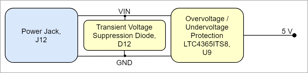 Image Added Image Added
|
|
Power Rails
| Scroll Title |
|---|
| anchor | Table_PWR_PR |
|---|
| title | Module Power Rails |
|---|
|
| Scroll Table Layout |
|---|
| orientation | portrait |
|---|
| sortDirection | ASC |
|---|
| repeatTableHeaders | default |
|---|
| style | |
|---|
| widths | |
|---|
| sortByColumn | 1 |
|---|
| tableStyling | confluence |
|---|
| sortEnabled | false |
|---|
| cellHighlighting | true |
|---|
|
| Connector Designator | VCCIO Schematic Name | Pin | VCC | Direction | Notes |
|---|
| J12 | VIN | 1 | 5 V | In |
| | J3 | 3.3V | 2, 4 | 3.3 V | Out |
| | 5V | 5 | 5 V | Out |
| | J5 | 3.3V | 3 | 3.3 V | Out |
|
|
Bank Voltages
| Scroll Title |
|---|
| anchor | Table_PWR_BV |
|---|
| title | Intel Cyclone 10 LP Bank Voltages |
|---|
|
| Scroll Table Layout |
|---|
| orientation | portrait |
|---|
| sortDirection | ASC |
|---|
| repeatTableHeaders | default |
|---|
| style | |
|---|
| widths | |
|---|
| sortByColumn | 1 |
|---|
| sortEnabled | false |
|---|
| cellHighlighting | true |
|---|
|
| Schematic Name | | Notes |
|---|
| Bank 1...8 | VCCIO1...8 | 3.3V |
|
|
Technical Specifications
Absolute Maximum Ratings
| Scroll Title |
|---|
| anchor | Table_TS_AMR |
|---|
| title | Absolute Maximum Ratings |
|---|
|
| Scroll Table Layout |
|---|
| orientation | portrait |
|---|
| sortDirection | ASC |
|---|
| repeatTableHeaders | default |
|---|
| style | |
|---|
| widths | |
|---|
| sortByColumn | 1 |
|---|
| sortEnabled | false |
|---|
| cellHighlighting | true |
|---|
|
| Symbols | Description | Min | Max | Unit | Note |
|---|
| VIN | Input Supply Voltage (J12)
| 4.5 | 5.5 | V |
| | AREF | External Reference Voltage for ADC/DAC (J1 - 8) | -0.3 | 3.6 | V | Only for input usage. | | AIN0...5 | Input Voltage for ADC/DAC (J4) | -0.3 | 3.6 | V | Only for input usage. | | AIN6...7 | Input Voltage for ADC/DAC (TP1...2) | -0.3 | 3.6 | V | Only for input usage. | | EXT_RST | External Reset (J3 - 3) | -0.5 | 4.2 | V |
| | D0_RXD, D1_TXD, D2...7 | Arduino Interface (J2) | -0.5 | 4.2 | V | Only for input usage. | D8...13, D14_SDA, D15_SCL | Arduino Interface (J1 - 1...6, 9...10) | -0.5 | 4.2 | V | Only for input usage. | | I2C_SCL, I2C_SDA | I2C Interface (J5 - 1...2) | -0.3 | 4.2 | V | Only for input usage. | P1_IO1...8, P2_IO1...8, P3_IO1...8, P4_IO1...8, P5_IO1...8, P6_IO1...8, | Pmod Interface (P1...6) | -0.5 | 4.2 | V | Only for input usage. | | CLK_IN | External FPGA Clock (J19) | -0.5 | 4.2 | V |
| | CLK_OUT | Clock / IO (J20) | -0.5 | 4.2 | V | Only for input usage. | | T_STG | Storage Temperature | -35 | 85 | °C | See LTC2623WC datasheet |
|
Recommended Operating Conditions
Operating temperature range depends also on customer design and cooling solution. Please contact us for options.
| Scroll Title |
|---|
| anchor | Table_TS_AMRROC |
|---|
| title | PS absolute maximum ratingsRecommended Operating Conditions |
|---|
|
| Scroll Table Layout |
|---|
| orientation | portrait |
|---|
| sortDirection | ASC |
|---|
| repeatTableHeaders | default |
|---|
| style | |
|---|
| widths | |
|---|
| sortByColumn | 1 |
|---|
| sortEnabled | false |
|---|
| cellHighlighting | true |
|---|
|
Symbols| Description | UnitVV | VVVV |
Recommended Operating Conditions
Operating temperature range depends also on customer design and cooling solution. Please contact us for options.
|
| | AIN0...5 | 0 | AREF | V |
|
| | AIN6...7 | 0 | AREF | V |
|
| | EXT_RST | -0.5 | 3.6 | V |
|
| | D0_RXD, D1_TXD, D2...7 | -0.5 | 3.6 | V |
|
| D8...13, D14_SDA, D15_SCL | -0.5 | 3.6 | V |
|
| | I2C_SCL, I2C_SDA | -0.3 | 3.3 | V |
|
| P1_IO1...8, P2_IO1...8, P3_IO1...8, P4_IO1...8, P5_IO1...8, P6_IO1...8, | -0.5 | 3.6 | V |
|
| | CLK_IN | -0.5 | 3.6 | V |
|
| | CLK_OUT | -0.5 | 3.6 | V |
|
| | T_OP | 0 | 70 | °C | See SDRAM W9864G6JT datasheet |
|
| Scroll Title |
|---|
| anchor | Table_TS_ROC |
|---|
| title | Recommended operating conditions. |
|---|
|
| Scroll Table Layout |
|---|
|
| orientation | portrait |
|---|
| sortDirection | ASC |
|---|
| repeatTableHeaders | default |
|---|
style | widths | | sortByColumn | 1 |
|---|
| sortEnabled | false |
|---|
| cellHighlighting | true |
|---|
| Parameter | Min | Max | Units | Reference Document |
|---|
V | See ???? datasheets. | V | See Xilinx ???? datasheet. | V | See Xilinx ???? datasheet. | V | See Xilinx ???? datasheet. | V | See Xilinx ???? datasheet. | V | See Xilinx ???? datasheet. | V | See Xilinx ???? datasheet. | °C | See Xilinx ???? datasheet. | °C | See Xilinx ???? datasheet.
Physical Dimensions
Module size: ?? 95 mm × ?? 110 mm. Please download the assembly diagram for exact numbers.Mating height with standard connectors: ? mm.
- PCB thickness:
...
| Page properties |
|---|
|
In 'Physical Dimension' section, top and bottom view of module must be inserted, information regarding physical dimensions can be obtained through webpage for product in Shop.Trenz, (Download> Documents> Assembly part) for every SoM. For Example: for Module TE0728, Physical Dimension information can be captured by snipping tools from the link below: https://www.trenz-electronic.de/fileadmin/docs/Trenz_Electronic/Modules_and_Module_Carriers/5.2x7.6/TE0745/REV02/Documents/AD-TE0745-02-30-1I.PDF
|
...
| Scroll Title |
|---|
| anchor | Figure_TS_PD |
|---|
| title | Physical Dimension |
|---|
|
| Scroll Ignore |
|---|
| draw.io Diagram |
|---|
| border | false |
|---|
| viewerToolbar | true |
|---|
| |
|---|
| fitWindow | false |
|---|
| diagramDisplayName | |
|---|
| lbox | true |
|---|
| revision | 23 |
|---|
| diagramName | TEI0009_TS_PD |
|---|
| simpleViewer | false |
|---|
width | | links | auto |
|---|
| tbstyle | hidden |
|---|
| diagramWidth | 640 |
|---|
|
|
| Scroll Only |
|---|
| scroll-pdf | true |
|---|
| scroll-office | true |
|---|
| scroll-chm | true |
|---|
| scroll-docbook | true |
|---|
| scroll-eclipsehelp | true |
|---|
| scroll-epub | true |
|---|
| scroll-html | true |
|---|
| 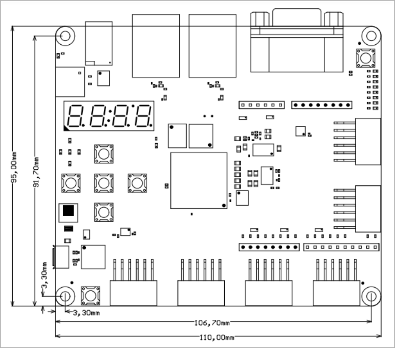 Image Removed Image Removed
|
|
Currently Offered Variants
| _PD | | simpleViewer | false |
|---|
| width | |
|---|
| links | auto |
|---|
| tbstyle | hidden |
|---|
| diagramWidth | 640 |
|---|
|
|
| Scroll Only |
|---|
| scroll-pdf | true |
|---|
| scroll-office | true |
|---|
| scroll-chm | true |
|---|
| scroll-docbook | true |
|---|
| scroll-eclipsehelp | true |
|---|
| scroll-epub | true |
|---|
| scroll-html | true |
|---|
| Image Added |
|
Currently Offered Variants
| Page properties |
|---|
|
Set correct link to the shop page overview table of the product on English and German. Example for TE0728: ENG Page: https://shop.trenz-electronic.de/en/Products/Trenz-Electronic/TE07XX-Zynq-SoC/TE0728-Zynq-SoC/ DEU Page: https://shop.trenz-electronic.de/de/Produkte/Trenz-Electronic/TE07XX-Zynq-SoC/TE0728-Zynq-SoC/ For Baseboards, where no overview page is available (and revision number is coded in the direct link) use shop search link, e.g. TE0706: ENG Page: https://shop.trenz-electronic.de/en/search?sSearch=TE0706 DEU Page: https://shop.trenz-electronic.de/de/search?sSearch=TE0706 if not available, set. |
| Page properties |
|---|
|
Set correct link to the shop page overview table of the product on English and German. Example for TE0728: ENG Page: enProducts/TE07XX-Zynq-SoCTE0728-Zynq-SoC/ DEU Page: deProdukteTE07XX-Zynq-SoC/TE0728-Zynq-SoC/For Baseboards, where no overview page is available (and revision number is coded in the direct link) use shop search link, e.g. TE0706: ENG Page: https://shop.trenz-electronic.de/en/search?sSearch=TE0706 DEU Page: https://shop.trenz-electronic.de/de/search?sSearch=TE0706 if not available, set. |
| Scroll Title |
|---|
| anchor | Table_VCP_SO |
|---|
| title | Trenz Electronic Shop Overview |
|---|
|
| Scroll Table Layout |
|---|
| orientation | portrait |
|---|
| sortDirection | ASC |
|---|
| repeatTableHeaders | default |
|---|
| style | |
|---|
| widths | |
|---|
| sortByColumn | 1 |
|---|
| sortEnabled | false |
|---|
| cellHighlighting | true |
|---|
|
|
Revision History
Hardware Revision History
| Scroll Title |
|---|
| anchor | Table_VCPRH_SOHRH |
|---|
| title | Trenz Electronic Shop Overview Hardware Revision History |
|---|
|
| Scroll Table Layout |
|---|
| orientation | portrait |
|---|
| sortDirection | ASC |
|---|
| repeatTableHeaders | default |
|---|
| style | |
|---|
| widths | |
|---|
| sortByColumn | 1 |
|---|
| sortEnabled | false |
|---|
| cellHighlighting | true |
|---|
|
|
| Trenz shop TE0728 overview page |
|---|
| English page | German page |
Revision History
Hardware Revision History
...
Set correct links to download arrier, e.g. TE0706 REV02:
...
| 1 |
|---|
| sortEnabled | false |
|---|
| cellHighlighting | true |
|---|
|
| Date | Revision | Changes | Document Link |
|---|
| 2018-2-19 | 01 | - | --- | | 2018-7-18 | 02 | - Change J5 from SMD Connector to GROVE Connector
- Change connection of 12 MHz clock from Bank 1 to Bank 6
- Change connection of I2C SDA/SCL from Bank 3 to Bank 6
- SMA Coaxial Connector J19, J20 not mounted
- Change connection of CLK_IN/CLK_OUT from Bank 4 to Bank 8
- Remove DIP Switch S1
- Add 5 LEDs (Red)
- Add 2 Push Buttons
- Add 64 Mbit QSPI Flash Memory
- Change SDRAM Memory
- Remove 10-Bit ADC
- Remove 10-Bit DAC
- Add 12-Bit ADC/DAC
- Remove USB Transceiver
- Remove 24 MHz Oscillator
- Remove DIP Switch S2
- Changed Power Supply Circuit
- Add 4 Pmod Host Sockets
| REV02 |
|
Hardware revision number can be found on the PCB board together with the module model number separated by the dash.
| Scroll Title |
|---|
| anchor | TableFigure_RHRV_HRHHRN |
|---|
| title | Board Hardware Revision HistoryNumber |
|---|
|
tablelayout |
| orientation | portrait |
|---|
| sortDirection | ASC |
|---|
| repeatTableHeaders | default |
|---|
style | widths | | sortByColumn | 1 |
|---|
| sortEnabled | false |
|---|
cellHighlightingDateRevisionChangesDocumentation Link- |
Hardware revision number can be found on the PCB board together with the module model number separated by the dash.
| true | | revision | 2 |
|---|
| diagramName | TEI0009 |
|---|
|
|
|
| Scroll Title |
|---|
| anchor | Figure |
|---|
| title | Board hardware revision number. |
|---|
| | simpleViewer | false |
|---|
| width | |
|---|
| links | auto |
|---|
| tbstyle | hidden |
|---|
| diagramWidth | 196 |
|---|
|
| | Scroll Ignore |
|---|
| Create DrawIO object here: Attention if you copy from other page, objects are only linked. |
| Scroll Only |
|---|
image link to the generate DrawIO PNG file of this page. This is a workaround until scroll pdf export bug is fixed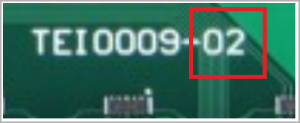 Image Added Image Added |
|
Document Change History
| Page properties |
|---|
|
- Note this list must be only updated, if the document is online on public doc!
- It's semi automatically, so do following
Add new row below first Copy "Page Information Macro(date)" Macro-Preview, Metadata Version number, Author Name and description to the empty row. Important Revision number must be the same as the Wiki document revision number Update Metadata = "Page Information Macro (current-version)" Preview+1 and add Author and change description. --> this point is will be deleted on newer pdf export template - Metadata is only used of compatibility of older exports
|
...
| Scroll Title |
|---|
| anchor | Table_RH_DCH |
|---|
| title | Document change history.Change History |
|---|
|
| Scroll Table Layout |
|---|
| orientation | portrait |
|---|
| sortDirection | ASC |
|---|
| repeatTableHeaders | default |
|---|
| style | |
|---|
| widths | |
|---|
| sortByColumn | 1 |
|---|
| sortEnabled | false |
|---|
| cellHighlighting | true |
|---|
|
| Date | Revision | Contributor | Description |
|---|
| Page info |
|---|
| infoType | Modified date |
|---|
| dateFormat | yyyy-MM-dd |
|---|
| type | Flat |
|---|
|
| | Page info |
|---|
| infoType | Current version |
|---|
| prefix | v. |
|---|
| type | Flat |
|---|
| showVersions | false |
|---|
|
| | Page info |
|---|
| infoType | Modified by |
|---|
| type | Flat |
|---|
| showVersions | false |
|---|
|
| - change listinitial release
| -- | all | | Page info |
|---|
| infoType | Modified users |
|---|
| type | Flat |
|---|
| showVersions | false |
|---|
|
| |
|
Disclaimer
| Include Page |
|---|
| IN:Legal Notices |
|---|
| IN:Legal Notices |
|---|
|
...