...
| Scroll Title |
|---|
| anchor | Figure_PWR_PD |
|---|
| title | Power Distribution |
|---|
|
| Scroll Ignore |
|---|
| draw.io Diagram |
|---|
| border | false |
|---|
| viewerToolbar | true |
|---|
| |
|---|
| fitWindow | false |
|---|
| diagramDisplayName | |
|---|
| lbox | true |
|---|
| revision | 47 |
|---|
| diagramName | TEI0009_PWR_PD |
|---|
| simpleViewer | false |
|---|
| width | |
|---|
| links | auto |
|---|
| tbstyle | hidden |
|---|
| diagramWidth | 639 |
|---|
|
|
| Scroll Only |
|---|
|
|
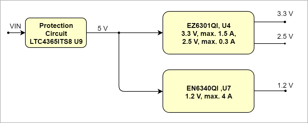
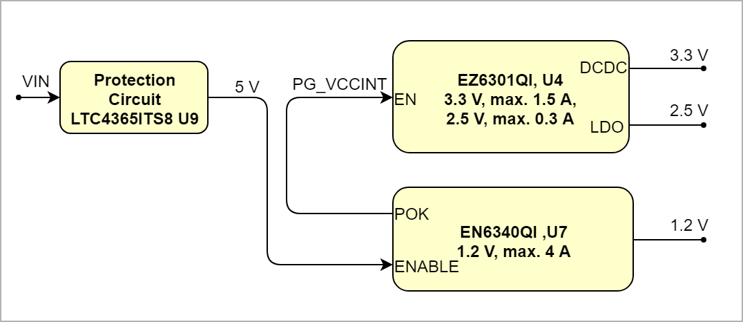
Power-On Sequence
There is no power on sequence, After power up regulators will be enabled as you can see in the diagram below.
| Scroll Title |
|---|
| anchor | Figure_PWR_PS |
|---|
| title | Power Sequency |
|---|
|
| Scroll Ignore |
|---|
| draw.io Diagram |
|---|
| border | false |
|---|
| viewerToolbar | true |
|---|
| |
|---|
| fitWindow | false |
|---|
| diagramDisplayName | |
|---|
| lbox | true |
|---|
| revision | 26 |
|---|
| diagramName | TEI0009_PWR_PS |
|---|
| simpleViewer | false |
|---|
| width | |
|---|
| links | auto |
|---|
| tbstyle | hidden |
|---|
| diagramWidth | 639 |
|---|
|
|
| Scroll Only |
|---|
|
|
Voltage Monitor Circuit
There is a diod (D12) which protects the board from wrong polarity, Additionaly there is an Over/under voltage (IC) which protects the board from over voltage damages.
| Scroll Title |
|---|
| anchor | Figure_PWR_VMC |
|---|
| title | Voltage Monitor Circuit |
|---|
|
| Scroll Ignore |
|---|
| draw.io Diagram |
|---|
| border | true |
|---|
| viewerToolbar | true |
|---|
| |
|---|
| fitWindow | false |
|---|
| diagramName | TEI0009_PWR_VM |
|---|
| simpleViewer | false |
|---|
| width | |
|---|
| diagramWidth | 641 |
|---|
| revision | 1 |
|---|
|
|
| Scroll Only |
|---|
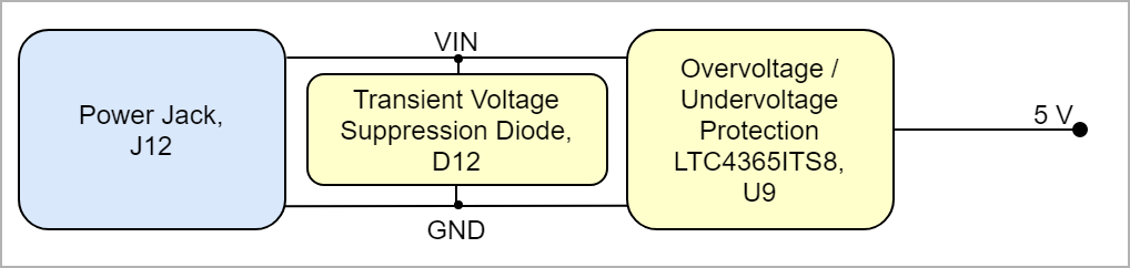 Image Added Image Added
| Create DrawIO object here: Attention if you copy from other page, objects are only linked. | | Scroll Only |
|---|
image link to the generate DrawIO PNG file of this page. This is a workaround until scroll pdf export bug is fixed |
|
Power Rails
| Scroll Title |
|---|
| anchor | Table_PWR_PR |
|---|
| title | Module power rails. |
|---|
|
| Scroll Table Layout |
|---|
| orientation | portrait |
|---|
| sortDirection | ASC |
|---|
| repeatTableHeaders | default |
|---|
| style | |
|---|
| widths | |
|---|
| sortByColumn | 1 |
|---|
| sortEnabled | false |
|---|
| cellHighlighting | true |
|---|
|
| Connector Designator | VCC / VCCIO Schematic Name | Pin | Direction | Notes |
|---|
| J3 | 3.3V | 2,4 | Out |
| | 5V | 5 | Out |
| | J5 | 3.3V | 3 | Out |
Power Rail Name | B2B Connector JM1 Pin | B2B Connector JM2 Pin | B2B Connector JM3 Pin | Direction | Notes
|
Bank Voltages
| Scroll Title |
|---|
| anchor | Table_PWR_BV |
|---|
| title | Zynq SoC bank voltages. |
|---|
|
| Scroll Table Layout |
|---|
| orientation | portrait |
|---|
| sortDirection | ASC |
|---|
| repeatTableHeaders | default |
|---|
| style | |
|---|
| widths | |
|---|
| sortByColumn | 1 |
|---|
| sortEnabled | false |
|---|
| cellHighlighting | true |
|---|
|
| Schematic Name | | Notes |
|---|
| Bank 1 | VCCIO1 | 3.3V |
| | Bank 2 | VCCIO2 | 3.3V |
| | Bank 3 | VCCIO3 | 3.3V |
| | Bank 4 | VCCIO4 | 3.3V |
| | Bank 5 | VCCIO5 | 3.3V |
| | Bank 6 | VCCIO6 | 3.3V |
| | Bank 7 | VCCIO7 | 3.3V |
| | Bank 8 | VCCIO8 | 3.3V |
|
|
Technical Specifications
Absolute Maximum Ratings
...