...
- Intel® Cyclone 10 LP [10CL055YU484C8G],
- Package: UBGA-484
- Speed Grade: 8 (Slowest)
- Temperature: 0 °C to 85° C
- Package compatible device 10CL016, 10CL040, 10CL055, 10CL080 as assembly variant on request is possible
- 16 MBit (2 MByte) flash memory Flash Memory (optional up to 32 MBit (4 MByte) possible)
- Integrated USB 2.0 -JTAG Programmer
- Pin Header connectorsConnectors
- 64 MBit (8 MByte) SDRAM, up to 512 MBit (64 MByte) memory mountable
- 64 MBit (8 MByte) User Quad-SPI Flash Memory, up to 128 MBit (16 MByte) memory mountable
- 64 MBit HyperRAM (Pseudo SRAM), up to 128 MBit (16 MByte) memory mountable
- 2x MAC address Address EEPROM
- 2x Fast Ethernet PHY (10/100 Mbps)
- 8-channelChannel, 12-bitBit, configurable ADC/DAC
- D-Sub connectorConnector
- 2x RJ45 connectorConnector
- LEDs:
- Status LEDs, Power LED
- 13x User LEDs
- 7-segment displaySegment Display
- Push buttonsButtons:
- 2x Reset Push buttonsButtons
- 5x User Push buttonsButtons
- I/O: X/X/X (IOs/Diff. Pairs/LVSC Pairs) → ab hier weiter
- Power Supply:
- 70 GPIO
- 5 V Power Supply
- Dimension: 95 mm x 110 mm
- Others:
- Reverse polarity of supply voltage protectionUnder/Over voltage protectionSupply Protection
- Undervoltage/Overvoltage Protection
Block Diagram
| Page properties |
|---|
|
add drawIO object here.
|
...
| Scroll Title |
|---|
| anchor | Figure_OV_BD |
|---|
| title | TEI0009 block diagram |
|---|
|
| Scroll Ignore |
|---|
| draw.io Diagram |
|---|
| border | false |
|---|
| viewerToolbar | true |
|---|
| |
|---|
| fitWindow | false |
|---|
| diagramDisplayName | |
|---|
| lbox | true |
|---|
| revision | 812 |
|---|
| diagramName | TEI0009_OV_BD |
|---|
| simpleViewer | false |
|---|
| width | |
|---|
| links | auto |
|---|
| tbstyle | hidden |
|---|
| diagramWidth | 641637 |
|---|
|
|
| Scroll Only |
|---|

|
|
Main Components
...
| Scroll Title |
|---|
| anchor | Figure_OV_BD |
|---|
| title | TEI0009 main components |
|---|
|
| Scroll Ignore |
|---|
| draw.io Diagram |
|---|
| border | false |
|---|
| viewerToolbar | true |
|---|
| |
|---|
| fitWindow | false |
|---|
| diagramDisplayName | |
|---|
| lbox | true |
|---|
| revision | 47 |
|---|
| diagramName | TEI0009_OV_MC |
|---|
| simpleViewer | false |
|---|
| width | |
|---|
| links | auto |
|---|
| tbstyle | hidden |
|---|
| diagramWidth | 640 |
|---|
|
|
| Scroll Only |
|---|
|
|
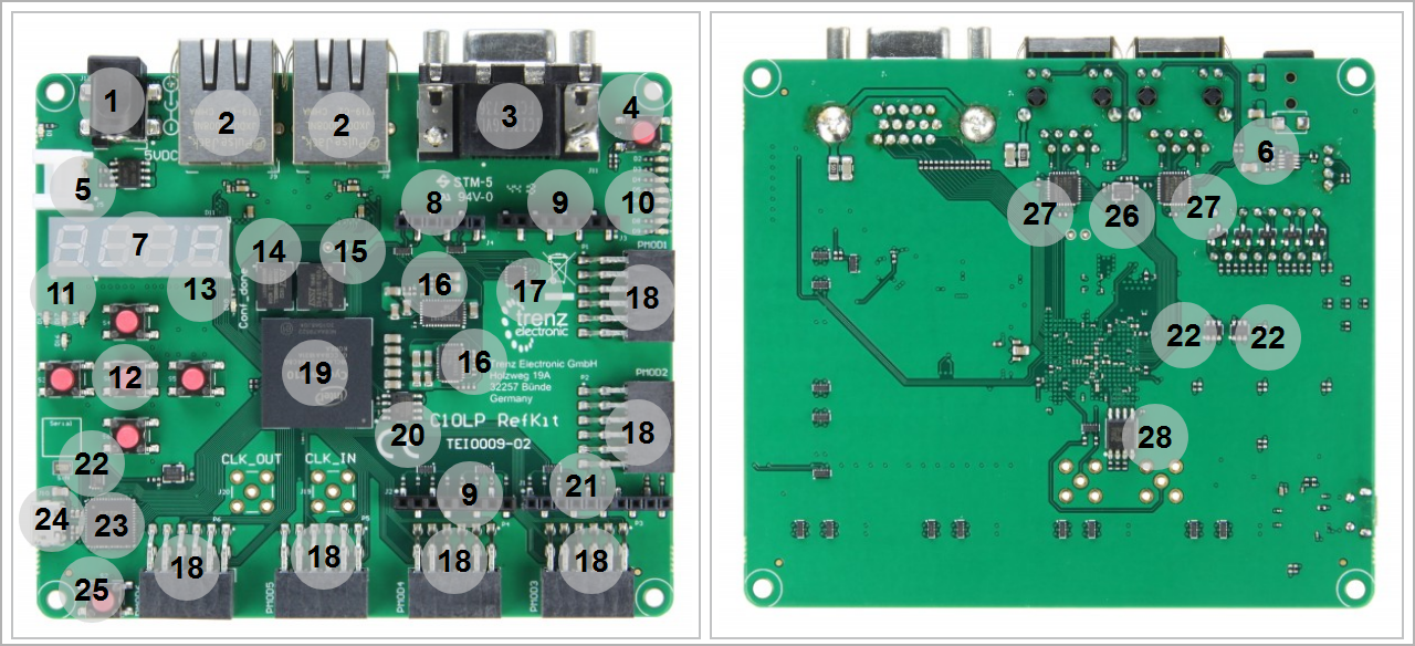
- Barrel Power Jack, J12
- RJ45 socketSocket, J8...9
- D-Sub Connector, J11
- Push buttonButton (Reset), S7
- Grove connectorConnector, J5
- Under/Over Voltage ProtecterUndervoltage/Overvoltage Protector, U9
- 7-segment Segment LED, D11
- 1x6 pin headerPin Header, J4
- 1x8 pin headerPin Header, J2...3
- 8x User LEDs (Red LEDs), D2...9
- 8x 5x User LEDs (Red LEDs), D13...17
- 5x User Push buttonsButtons, S1- S3...6
- Red LED (CONF_DONE), D10
- PSRAM memoryMemory, U3
- SDRAM memoryMemory, U10
- Voltage Regulator, U5U4 - U7
- AD/DA ConvertorConverter, U2
- Pmod 2x6 SMD host socket6x Pmod Host Socket, P1...6
- Intel®Cyclone Intel® Cyclone 10 LP, U1
- Serial Configuration memoryMemory, U5
- 1x10 pin headerPin Header, J1
- EEEPROM, U15 - U18 - U20
- FTDI USB2 to JTAG/UART adapterConverter, U14
- Micro USB 2.0 (receptacle) , J10
- Push button Button (RST_GPIO), S2
- Oscillator, U22
- Ethernet PHY, U17 - U19
- QSPI Flash memoryMemory, U12
Initial Delivery State
...
| Scroll Title |
|---|
| anchor | Table_OV_IDS |
|---|
| title | Initial delivery state of programmable devices on the module |
|---|
|
| Scroll Table Layout |
|---|
| orientation | portrait |
|---|
| sortDirection | ASC |
|---|
| repeatTableHeaders | default |
|---|
| style | |
|---|
| widths | |
|---|
| sortByColumn | 1 |
|---|
| sortEnabled | false |
|---|
| cellHighlighting | true |
|---|
|
Storage device name | Content | Notes |
|---|
QSPI Flash (U12) | Not programmed |
| | EEPROM (U15) | Programmed | FTDI configuration | | SDRAMEEPROM (U18, U20) | Not programmedPSRAM | Except Ethernet MAC | | SDRAM (U10) | Not programmedFTDI System Controller CPLD |
| | PSRAM (U3) | Not programmed |
| | Serial Configuration Memory (U5) | Programmed |
|
|
Configuration Signals
...
| Scroll Title |
|---|
| anchor | Table_OV_BP |
|---|
| title | Boot process. |
|---|
|
| Scroll Table Layout |
|---|
| orientation | portrait |
|---|
| sortDirection | ASC |
|---|
| repeatTableHeaders | default |
|---|
| style | |
|---|
| widths | |
|---|
| sortByColumn | 1 |
|---|
| sortEnabled | false |
|---|
| cellHighlighting | true |
|---|
|
MODE Signal State | MSEL0 | MSEL1 | MSEL2 | MSEL3 | Connected to | Boot Mode |
|---|
MSEL[0:3] | 0 | 1 | 0 | 0 | Bank 6 | AS (Active Serial) |
|
RESET pin can be set through the push button S1.
| Scroll Title |
|---|
| anchor | Table_OV_RST |
|---|
| title | Reset process. |
|---|
|
| Scroll Table Layout |
|---|
| orientation | portrait |
|---|
| sortDirection | ASC |
|---|
| repeatTableHeaders | default |
|---|
| style | |
|---|
| widths | |
|---|
| sortByColumn | 1 |
|---|
| sortEnabled | false |
|---|
| cellHighlighting | true |
|---|
|
Signal | Connected to | Note |
|---|
RESET | S7 (Push button) | Connected to nCONFIG | RST_GPIO | S2 (Push button) | EXT_RST | J3 (1x8 pin header) Bank 2. |
|
Signals, Interfaces and Pins
...
| Scroll Title |
|---|
| anchor | Table_SIP_B2B |
|---|
| title | General I/O to Pin header and Pmod SMD connectors information |
|---|
|
| Scroll Table Layout |
|---|
| orientation | portrait |
|---|
| sortDirection | ASC |
|---|
| repeatTableHeaders | default |
|---|
| style | |
|---|
| widths | |
|---|
| sortByColumn | 1 |
|---|
| sortEnabled | false |
|---|
| cellHighlighting | true |
|---|
|
| FPGA Bank | Connector | I/O Signal Count | Voltage Level | Notes |
|---|
| Bank 1 | J1 (Pin header) | 8 Single ended | 3.3 V |
| | J2 (Pin header) | 8 Single ended | 3.3 V |
| | J4 (Pin header) | 6 Single ended | 3.3 V |
| | Bank 2 | J3 (Pin header) | 1 Single ended | 3.3 V |
| | P1 (PMod SMD host socketPmod Host Socket) | 8 Single ended | 3.3 V |
| | P2 (PMod SMD host socketPmod Host Socket) | 8 Single ended | 3.3 V |
| | J11 (VGA host Socket) | 14 Single ended | 3.3 V |
| | Bank 6 | J5 (Grove connector) | 2 Single ended | 3.3 V |
| | Bank 7 | P5 (PMod SMD host socketPmod Host Socket) | 8 Single ended | 3.3 V |
| | P6 (PMod SMD host socketPmod Host Socket) | 8 Single ended | 3.3 V |
| | Bank 8 | P3 (PMod SMD host socketPmod Host Socket) | 8 Single ended | 3.3 V |
| | P4 (PMod SMD host socketPmod Host Socket) | 8 Single ended | 3.3 V |
|
...
Pmod Host Socket
TEI0009 has 6 PMod 2x6 SMD Host Socket 90° 6 Pmod 2x6 host sockets which are connected to Cyclon 10 LP (U1).
| Scroll Title |
|---|
| anchor | Table_SIP_SMD |
|---|
| title | PMod SMD host socket information |
|---|
|
| Scroll Table Layout |
|---|
| orientation | portrait |
|---|
| sortDirection | ASC |
|---|
| repeatTableHeaders | default |
|---|
| style | |
|---|
| widths | |
|---|
| sortByColumn | 1 |
|---|
| sortEnabled | false |
|---|
| cellHighlighting | true |
|---|
|
| Designator | Signals | Connected to | Notes |
|---|
| P1 | P1_IO1...8 | Bank 2 |
| | P2 | P2_IO1...8 | Bank 2 |
| | P3 | P3_IO1...8 | Bank 8 |
| | P4 | P4_IO1...8 | Bank 8 |
| | P5 | P5_IO1...8 | Bank 7 |
| | P6 | P6_IO1...8 | Bank 7 |
|
UART Interface
UART access to TEI0009 is available on 1x8 pin header J2.
...
| anchor | Table_SIP_UART |
|---|
| title | UART interface information |
|---|
TEI0009 has 5 pin headers. The pin headers J1...4 are usable for Arduino modules, too.
...
| tablelayout |
|---|
| orientation | portrait |
|---|
| sortDirection | ASC |
|---|
| repeatTableHeaders | default |
|---|
| style | |
|---|
| widths | |
|---|
| sortByColumn | 1 |
|---|
| sortEnabled | false |
|---|
| cellHighlighting | true |
|---|
|
...
| Scroll Title |
|---|
| anchor | Table_SIP_J1 |
|---|
| title | Pin Header J1 |
|---|
|
| Pin Header J1 | Signals | Connected to | Notes |
|---|
| J1 - 1...6 | D8...13 | Bank 1 |
| | J1 - 7 | GND |
|
| | J1 - 8 | AREF | ADC/DAC |
| | J1 - 9 | D14_SDA | Bank 1 |
| | J1 - 10 | D14_SCL | Bank 1 |
|
|
| Scroll Title |
|---|
| anchor | Table_SIP_J2 |
|---|
| title | Pin Header J2 |
|---|
|
| Scroll Table Layout |
|---|
| orientation | portrait |
|---|
| sortDirection | ASC |
|---|
| repeatTableHeaders | default |
|---|
| style | |
|---|
| widths | |
|---|
| sortByColumn | 1 |
|---|
| sortEnabled | false |
|---|
| cellHighlighting | true |
|---|
|
| Pin Header J2 | Signals | Connected to | Notes |
|---|
| J2 - 1 | D0_RXD | Bank 1 |
| | J2 - 2 | D1_TXD | Bank 1 |
| | J2 - 3...8 | D2...4 | Bank 1 |
|
|
| Scroll Title |
|---|
| anchor | Table_SIP_J3 |
|---|
| title | Pin Header J3 |
|---|
|
| Scroll Table Layout |
|---|
| orientation | portrait |
|---|
| sortDirection | ASC |
|---|
| repeatTableHeaders | default |
|---|
| style | |
|---|
| widths | |
|---|
| sortByColumn | 1 |
|---|
| sortEnabled | false |
|---|
| cellHighlighting | true |
|---|
|
| Pin Header J3 | Signals | Connected to | Notes |
|---|
| J2 - 1 | NC | - |
| | J3 - 2 | 3.3V | 3.3 V |
| | J3 - 3 | EXT_RST | Bank 2 | Pulled- up to 3.3 V | | J3 - 4 | 3.3V | 3.3 V |
| | J3 - 5 | 5V | 5 V |
| | J3 - 6...7 | GND | GND |
| | J2 - 8 | NC | - |
|
|
| Scroll Title |
|---|
| anchor | Table_SIP_J4 |
|---|
| title | Pin Header J4 |
|---|
|
| Scroll Table Layout |
|---|
| orientation | portrait |
|---|
| sortDirection | ASC |
|---|
| repeatTableHeaders | default |
|---|
| style | |
|---|
| widths | |
|---|
| sortByColumn | 1 |
|---|
| sortEnabled | false |
|---|
| cellHighlighting | true |
|---|
|
| Pin Header J4 | Signals | Connected to | Notes |
|---|
| J4 - 1...6 | AIN0...5 | FPGA Bank 1 and ADC/DAC |
|
|
...
Micro USB2.0 Connector
U14(FTDI FT2232) can be accessed through Micro USB2.0 B Receptacle 90 (J10).
| Scroll Title |
|---|
| anchor | Table_SIP_USBJ5 |
|---|
| title | Micro USB2.0 B Receptacle 90 ° informationPin Header J5 |
|---|
|
| Scroll Table Layout |
|---|
| orientation | portrait |
|---|
| sortDirection | ASC |
|---|
| repeatTableHeaders | default |
|---|
| style | |
|---|
| widths | |
|---|
| sortByColumn | 1 |
|---|
| sortEnabled | false |
|---|
| cellHighlighting | true |
|---|
|
Schematic| Voltage Level | Notes | USB_VBUS | GND | D- | U14 (FTDI FT2232) | 3.3 V | D+ | U14 (FTDI FT2232) | 3.3 V | Notes |
|---|
| J5 - 1 | I2C_SCL | FPGA Bank 6 and EEPROM (U18,U20) | Pulled-up to 3.3V. | | J5 - 2 | I2C_SDA | FPGA Bank 6 and EEPROM (U18,U20) | Pulled-up to 3.3V. | | J5 - 3 | 3.3V | 3.3 V |
| | J5 - 4 | GND | GND |
|
|
Micro USB 2.0 Connector
FTDI FT2232 (U14) can be accessed through micro USB 2.0 B connector (J10) for JTAG (channel A). Channel B is connected to the FPGA and can be used for UART or other standards.
RJ45 Connectors
TEI0009 is equipped with two RJ45 connectors and two Ethernet PHYs. RJ45 connectors J8 and J9 are connected to Ethernet PHYs U17 and U19 respectively. .
| Scroll Title |
|---|
| anchor | Table_SIP_RJ45 |
|---|
| title | RJ45 connectors information |
|---|
|
| Scroll Table Layout |
|---|
| orientation | portrait |
|---|
| sortDirection | ASC |
|---|
| repeatTableHeaders | default |
|---|
| style | |
|---|
| widths | |
|---|
| sortByColumn | 1 |
|---|
| sortEnabled | false |
|---|
| cellHighlighting | true |
|---|
|
| Pin | Schematic | ETH1 Pin | ETH2 Pin | Notes |
|---|
| TD+ |
ETH| ETH1_TX_P, ETH2_TX_P | U17 - TXP | U19 - TXP |
| | CT |
ETH| ETH1_CTREF_TCT, ETH2_CTREF_TCT | - | - |
Connected to GNDETH| ETH1_TX_N, ETH2_TX_N | U17 - TXM | U19 - TXM |
| | RD+ |
ETH| ETH1_RX_P, ETH2_RX_P | U17 - RXP | U19 - RXP |
| | CT |
ETH| ETH1_CTREF_RCT, ETH2_CTREF_RCT | - | - |
Connected to GNDETH| ETH1_RX_N, ETH2_RX_N | U17 - RXM | U19 - RXM |
| | LED Green |
ETH| ETH1_LED0, ETH2_LED0 | U17 - |
NWAYEN NWAYENETH| ETH1_LED1, ETH2_LED1 | U17 - |
SPEED SPEED
|
D-Sub Connectors
TEI0009 is equipped with a D-Sub connector (Receptacle) which provides interface to Cyclone 10 LP through Bank 2.
...
| Scroll Title |
|---|
| anchor | Table_OBP |
|---|
| title | On board peripherals |
|---|
|
| Scroll Table Layout |
|---|
| orientation | portrait |
|---|
| sortDirection | ASC |
|---|
| repeatTableHeaders | default |
|---|
| style | |
|---|
| widths | |
|---|
| sortByColumn | 1 |
|---|
| sortEnabled | false |
|---|
| cellHighlighting | true |
|---|
|
|
QSPI Flash Memory
| Page properties |
|---|
|
Notes : Minimum and Maximum density of quad SPI flash must be mentioned for other assembly options. |
There is a 64MBit (8 MByte) QSPI Flash memory (U12) provided by Winbond Integrated Silicon Solution Inc. which can be used to store data or configuration. Up to 128 MBit (16 MByte) memory is possible on other assembly option.
| Scroll Title |
|---|
| anchor | Table_OBP_SPI |
|---|
| title | Quad SPI interface MIOs and pins |
|---|
|
| Scroll Table Layout |
|---|
| orientation | portrait |
|---|
| sortDirection | ASC |
|---|
| repeatTableHeaders | default |
|---|
| style | |
|---|
| widths | |
|---|
| sortByColumn | 1 |
|---|
| sortEnabled | false |
|---|
| cellHighlighting | true |
|---|
|
| Pin | Schematic | Connected to | Notes |
|---|
| CS | F_CS | Bank 7 |
| | CLK | F_CLK | Bank 7 |
| | IO0...3 | F_IO0...3 | Bank 7 |
|
|
...
| Page properties |
|---|
|
Notes : Minimum and Maximum density of DDR3 SDRAM must be mentioned for other assembly options. (pay attention to supported address length for DDR3) |
The TEI0009 has 256 MBit volatile provided by Winbond 64 MBit (8 MByte) volatile memory provided by Integrated Silicon Solution Inc., SDRAM IC(U10) for storing user application code and data. Up to 512 MBit (64 MByte) SDRAM is possibleon possible on other assembly option.
Part number: W9864G6JTIS42S16400J-6-ND7BL
Supply voltage: 3.3 V
- Clock Frequency: 166MHz143 MHz (optional up to 200 MHz)
Temperature: 0°C ~ 70°Cto 70°C (optional other ranges are available)
PSRAM Memory
The TEI0009 is integrated with 64Mbit 64 Mbit (8 MByte) Pseudo Static Random Access Memory (PSRAM) using a self-refresh DRAM array organized as 8M words by 8 bits. The device supports a HyperBus interface, Very Low Signal Count (Address, Command and data through 8 DQ pins), Hidden Refresh Operation, and Automotive Temperature Operation. Up to 128 MBit (16 MByte) memory is possible on other assembly option.
Part number: IS66WVH8M8BLL
Supply voltage: 3.3 V
- Clock Frequency: 100MHz100 MHz
Temperature: -40°C ~ 85°Cto 85°C (optional other ranges are available)
7-Segment
...
Display
The TEI0009 has a LED 4-Digit-7-Segment - 4 Digit LED display which is connected to Bank 6.
...
The FTDI chip U14 converts signals from USB2USB 2.0 to a variety of standard serial and parallel interfaces. Refer to the FTDI data sheet to get for more information about the capacity of the FT2232H chip.
Channel A of FTDI FT2232H chip is used in MPPSE mode for JTAG, 6 I/O's of . Channel B are is routed to FPGA bank 8 of the FPGA SoC and are usable for example as GPIOs, UART or 6 and is usable for other standard interfaces.
...
| Scroll Title |
|---|
| anchor | Table_OBP_FTDI |
|---|
| title | FTDI chip interfaces and pins |
|---|
|
| Scroll Table Layout |
|---|
| orientation | portrait |
|---|
| sortDirection | ASC |
|---|
| repeatTableHeaders | default |
|---|
| style | |
|---|
| widths | |
|---|
| sortByColumn | 1 |
|---|
| sortEnabled | false |
|---|
| cellHighlighting | true |
|---|
|
| FTDI Chip Pin | Signal Schematic Name | Connected to | Notes |
|---|
| ADBUS0 | TCK | Bank 1 | JTAG interface | | ADBUS1 | TDI | Bank 1 | | ADBUS2 | TDO | Bank 1 | | ADBUS3 | TMS | Bank 1 | | BDBUS0...7 | BDBUS0...7 | Bank 6 |
BDBUS1 | BDBUS1 | Bank 6 | BDBUS2 | BDBUS2 | Bank 6 | BDBUS3 | BDBUS3 | Bank 6 | BDBUS4 | BDBUS4 | Bank 6 | BDBUS5 | BDBUS5
| | BCBUS0...7 | BCBUS0...7 | Bank 6 |
| | EECS | EECS | EEPROM, U15 |
(EEPROM) (EEPROM) (EEPROM)U16 (12MHz Oscillator)| 12 MHz Oscillator, U16 |
| | DM | D_N |
J10 ( USB2)J10 ( USB2)
|
Serial Configuration Memory
On-board serial configuration memory (U5) is provided by Intel with 16 MBit (2 MByte) storage capacity. This non volatile memory is used to store initial FPGA configuration via JTAG interface. The memory is connected to FPGA bank 1 via active serial (AS) x1 interface.
| Scroll Title |
|---|
| anchor | Table_OBP_EEP |
|---|
| title | FTDI and EEPROM pin connections |
|---|
|
| Scroll Table Layout |
|---|
| orientation | portrait |
|---|
| sortDirection | ASC |
|---|
| repeatTableHeaders | default |
|---|
| style | |
|---|
| widths | |
|---|
| sortByColumn | 1 |
|---|
| sortEnabled | false |
|---|
| cellHighlighting | true |
|---|
|
| Configuration Memory Pin | Signal Schematic Name | Connected to | Notes |
|---|
| DATA1 | AS_DATA0 | U1, Bank 1
| Data out
|
| | DATA0 | AS_ASDO | U1, Bank 1 | Data in |
| | nCS | AS_NCSnCS | U1, Bank 1 | chip select |
| | DCLK | AS_DCLK | U1, Bank 1 | clock |
|
|
Ethernet PHY
The TEI0009 is equipped with two Ethernet PHY (U17, U19, U17) which are connected to two RJ45 (J8, J9) connectors.
| Scroll Title |
|---|
| anchor | Table_OBP_ETH |
|---|
| title | Ethernet PHY connections and pins |
|---|
|
| Scroll Table Layout |
|---|
| orientation | portrait |
|---|
| sortDirection | ASC |
|---|
| repeatTableHeaders | default |
|---|
| style | |
|---|
| widths | |
|---|
| sortByColumn | 1 |
|---|
| sortEnabled | false |
|---|
| cellHighlighting | true |
|---|
|
| Ethernet PHY Pin | Signal Schematic Names (ETH1/ETH2) | ETH 1 | ETH 2 | Note |
|---|
| TXD0...3 |
ETH| ETH1_TXD0...3, ETH2_TXD0...3 | Bank 5 | Bank 5 |
| | TXC |
ETH| ETH1_TXC, ETH2_TXC | Bank 5 | Bank 5 |
| | TXEN |
ETH| ETH1_TXEN, ETH2_TXEN | Bank 5 | Bank 5 |
| | RXD0...3 |
ETH| ETH1_RXD0...3, ETH2_RXD0...3 | Bank 5 | Bank 5 |
| | RXC/ |
/ETH| ETH1_RXC, ETH2_RXC | Bank 5 | Bank 5 |
| | RXER/ISO |
ETH| ETH1_RXER, ETH2_RXER | Bank 5 | Bank 5 |
| | INTRP/ |
/NANDETH| ETH1_INTRP, ETH2_INTRP | Bank 5 | Bank 5 |
| | XI |
ETH| ETH1_CLKIN, ETH2_CLKIN | Oscillator, U22 |
() (Oscillator)ETH| ETH1_MDC, ETH2_MDC | Bank 5 | Bank 5 |
| | MDIO |
ETH| ETH1_MDIO, ETH2_MDIO | Bank 5 | Bank 5 |
| | COL/CONFIG0 |
ETH| ETH1_COL, ETH2_COL | Bank 5 | Bank 5 |
| | CRS/CONFIG1 |
ETH| ETH1_CRS, ETH2_CRS | Bank 5 | Bank 5 |
| | RXDV/CONFIG2 |
ETH| ETH1_RXDV, ETH2_RXDV | Bank 5 | Bank 5 |
| | LED0/NWAYEN |
ETHBank 5J8B ()Bank 5 J9B ()ETHBank 5J8C (Bank 5 J9B ())ETH| ETH1_RST, ETH2_RST | Bank 5 | Bank 5 |
| | RXM |
ETH| ETH1_RX_N, ETH2_RX_N | RJ45, J8 |
(RJ45)J9 ()ETHJ8 ()J9 ()ETHJ8 ()J9 ()ETHJ8 ()J9 ()
|
EEPROM
TEI0009 has three EEPROM, U15, U18 and U20. U15 is pre-programmed by for the FTDI FT2232H configuration. U18 and U19 are used for the MAC address configuration.
| Scroll Title |
|---|
| anchor | Table_OBP_EEP |
|---|
| title | FTDI and EEPROM pin connections |
|---|
|
| Scroll Table Layout |
|---|
| orientation | portrait |
|---|
| sortDirection | ASC |
|---|
| repeatTableHeaders | default |
|---|
| style | |
|---|
| widths | |
|---|
| sortByColumn | 1 |
|---|
| sortEnabled | false |
|---|
| cellHighlighting | true |
|---|
|
| Designator | EEPROM Pin | Signal Schematic Names | Connected to | Notes |
|---|
| U15 | CS | EECS | FTDI, U14 (FTDI) |
| | CLK | |EECLK | FTDI, U14 (FTDI) |
| | DIN/DOUT | EEDATA | U14 (FTDI) | FTDI ConfigurationFTDI, U14 |
|
|
| Scroll Title |
|---|
| anchor | Table_OBP_EEP |
|---|
| title | I2C EEPROM interface MIOs and pins |
|---|
|
| Scroll Table Layout |
|---|
| orientation | portrait |
|---|
| sortDirection | ASC |
|---|
| repeatTableHeaders | default |
|---|
| style | |
|---|
| widths | |
|---|
| sortByColumn | 1 |
|---|
| sortEnabled | false |
|---|
| cellHighlighting | true |
|---|
|
| Designator | Pin | Schematic | Connected to | Grove Header | Notes |
|---|
| U18, U20 | SCL | I2C_SCL | Bank 6 | J5 |
| | SDA | I2C_SDA | Bank 6 | J5 |
|
|
...
| Scroll Title |
|---|
| anchor | Table_OBP_I2C_EEPROM |
|---|
| title | I2C address for EEPROM |
|---|
|
| Scroll Table Layout |
|---|
| orientation | portrait |
|---|
| sortDirection | ASC |
|---|
| repeatTableHeaders | default |
|---|
| style | |
|---|
| widths | |
|---|
| sortByColumn | 1 |
|---|
| sortEnabled | false |
|---|
| cellHighlighting | true |
|---|
|
| I2C Address | Designator | Notes |
|---|
| 0x50 | U18 |
| | 0x520x51 | U20 |
|
|
ADC/DAC
The TEI0009 module is equipped with 12bit a 12 bit ADC/DAC (U2).
| Scroll Title |
|---|
| anchor | Table_OBP_A2D |
|---|
| title | ADC/DAC interface and pins |
|---|
|
| Scroll Table Layout |
|---|
| orientation | portrait |
|---|
| sortDirection | ASC |
|---|
| repeatTableHeaders | default |
|---|
| style | |
|---|
| widths | |
|---|
| sortByColumn | 1 |
|---|
| sortEnabled | false |
|---|
| cellHighlighting | true |
|---|
|
| Pins | Schematic | Connected to | Notes |
|---|
nRESET | ADDA_RSTN | U1, Bank 2, U1 | VREF_ADC |
| | nSYNC | ADDA_SYNC | U1, Bank 2, U1 |
| | SCLK | MCLK | U1, Bank 2, U1 |
| | SDI | MSDIMOSI | U1, Bank 2, U1 |
| | SDO | MSDOMISO | U1, Bank 2, U1 |
| | VREF | -AREF | U1Pin Header, Bank 2J1 | External reference is 1 V to 3.3 V.3V → ???
Internal reference is 2.5 V. | | IO0...5 | AIN0...5 | U1, Bank 1, U1 Pin Header, J4, Pin header |
|
|
LEDs
| Scroll Title |
|---|
| anchor | Table_OBP_LED |
|---|
| title | On-board LEDs |
|---|
|
| Scroll Table Layout |
|---|
| orientation | portrait |
|---|
| sortDirection | ASC |
|---|
| repeatTableHeaders | default |
|---|
| style | |
|---|
| widths | |
|---|
| sortByColumn | 1 |
|---|
| sortEnabled | false |
|---|
| cellHighlighting | true |
|---|
|
| Schematic | Designator | Color | Connected to | Active Level | Note |
|---|
| LED1...8 | D2...9 | Red | Bank 3 | High |
| | LED_PB1 | D13...17 | Red | Bank 7 | High |
| | CONF_DONE | D10 | Red | Bank 6 | Low |
|
|
...