The Cyclone10 Cyclone 10 LP Reference Kit is the world's first development board with a 55 kLE (Logic Elements) Intel Cyclone 10 LP and a variety of interfaces for numerous applications.The board is comprehensively tested and ready for use with end products and can also be ordered in customer-specific variants according to your requirements.
...
Page properties
hidden
true
id
Comments
Note: 'Key Features' description: Important components and connector or other Features of the module → please sort and indicate assembly options
Intel® Cyclone 10 LP LP [10CL055YU484C8G],
Package: UBGA-484
Speed Grade: 8 (Slowest)
Temperature: 0 °C to 85° C
Package compatible device 10CL016, 10CL040, 10CL055, 10CL080 as assembly variant on request is possible
16 MBit (2 MByte) Flash Memory (optional up to 32 MBit (4 MByte)possible)
Integrated USB-JTAG Programmer
Pin Header Connectors
64 MBit (8 MByte) SDRAM , (optional up to 512 MBit (64 MByte)memory mountable)
64 MBit (8 MByte) User Quad-SPI Flash Memory , (optioneal up to 128 MBit (16 MByte))memory mountable
64 MBit (8 MByte) HyperRAM (Pseudo SRAM) , (optional up to 128 MBit (16 MByte)memory mountable)
2x MAC Address EEPROM
2x Fast Ethernet PHY (10/100 Mbps)
8-Channel, 12-Bit, configurable ADC/DAC
D-Sub Connector
2x RJ45 Connector
LEDs:
Status LEDs, Power LED
13x User LEDs
7-Segment Display
Push Buttons:
2x Reset Push Buttons
5x User Push Buttons
I/O: 70 GPIO
5 V Power Supply
Dimension: 95 mm x 110 mm
Others:
Reverse Supply Protection
Undervoltage/Overvoltage Protection
...
Scroll Title
anchor
Figure_OV_BD
title
TEI0009 block diagram
Scroll Ignore
draw.io Diagram
border
false
viewerToolbar
true
fitWindow
false
diagramDisplayName
lbox
true
revision
1214
diagramName
TEI0009_OV_BD
simpleViewer
false
width
links
auto
tbstyle
hidden
diagramWidth
637
Scroll Only
...
Power Jack, J12
RJ45 Socket, J8...9
D-Sub Connector, J11
Push Button (Reset), S7
Grove Connector, J5
Undervoltage/Overvoltage Protector, U9
7-Segment LED, D11
1x6 Pin Header, J4
1x8 Pin Header, J2...3
8x User LEDs (Red), D2...9
5x User LEDs (Red), D13...17
5x User Push Buttons, S1 - S3...6
Red LED (CONF_DONE), D10
PSRAM Memory, U3
SDRAM Memory, U10
Voltage Regulator, U4 - U7
AD/DA Converter, U2
6x Pmod Host Socket, P1...6
Intel® Cyclone 10 LP, U1
Serial Configuration Memory, U5
1x10 Pin Header, J1
EEEPROMEEPROM, U15 - U18 - U20
FTDI USB2 USB 2 to JTAG/UART Converter, U14
Micro USB 2.0, J10
Push Button (RST_GPIO), S2
Oscillator, U22
Ethernet PHY, U17 - U19
QSPI Flash Memory, U12
...
Scroll Title
anchor
Table_OV_RST
title
Reset process.
Scroll Table Layout
orientation
portrait
sortDirection
ASC
repeatTableHeaders
default
style
widths
sortByColumn
1
sortEnabled
false
cellHighlighting
true
Signal
Connected to
Note
RESET
S7 (Push button)S7, Push Button
Connected to nCONFIG.
Signals, Interfaces and Pins
...
FPGA bank number and number of I/O signals connected to the B2B connectorconnectors:
Scroll Title
anchor
Table_SIP_B2B
title
General I/O to Pin header Header and Pmod SMD connectors information
Scroll Table Layout
orientation
portrait
sortDirection
ASC
repeatTableHeaders
default
style
widths
sortByColumn
1
sortEnabled
false
cellHighlighting
true
FPGA Bank
Connector
I/O Signal Count
Voltage Level
Notes
Bank 1
J1 (Pin header)
8 Single ended
3.3 V
J2 (Pin header)
8 Single ended
3.3 V
J4 (Pin header)
6 Single ended
3.3 V
Bank 2
J3 (Pin header)
1 Single ended
3.3 V
P1 (Pmod Host Socket)
8 Single ended
3.3 V
P2 (Pmod Host Socket)
8 Single ended
3.3 V
J11 (VGA host Host Socket)
14 Single ended
3.3 V
Bank 6
J5 (Grove connectorConnector)
2 Single ended
3.3 V
Bank 7
P5 (Pmod Host Socket)
8 Single ended
3.3 V
P6 (Pmod Host Socket)
8 Single ended
3.3 V
Bank 8
P3 (Pmod Host Socket)
8 Single ended
3.3 V
P4 (Pmod Host Socket)
8 Single ended
3.3 V
...
Scroll Title
anchor
Table_SIP_VGA
title
VGA host socket information
Scroll Table Layout
orientation
portrait
sortDirection
ASC
repeatTableHeaders
default
style
widths
sortByColumn
1
sortEnabled
false
cellHighlighting
true
Schematic
Corresponding Signals
Connected to
Notes
VGA_RED
VGA_R0...3
Bank 2
Red channelChannel
VGA_GREEN
VGA_G0...3
Bank 2
Green channelGreen Channel
VGA_BLUE
VGA_B0...3
Bank 2
Blue channelBlue Channel
VGA_RGB_HSYNC
VGA_HS
Bank 2
Horizontal syncSync
VGA_RGB_VSYNC
VGA_VS
Bank 2
Vertical syncSync
On-board Peripherals
Page properties
hidden
true
id
Comments
Notes :
add subsection for every component which is important for design, for example:
Minimum and Maximum density of quad SPI flash must be mentioned for other assembly options.
There is a 64MBit 64 MBit (8 MByte) QSPI Flash memory (U12) provided by Integrated Silicon Solution Inc. which can be used to store data or configuration. Up to 128 MBit (16 MByte) memory is possible available on other assembly option.
...
The TEI0009 has 64 MBit (8 MByte) volatile memory provided by Integrated Silicon Solution Inc., SDRAM IC(U10) for storing user application code and data. Up to 512 MBit (64 MByte) SDRAM is possible available on other assembly option.
...
The TEI0009 is integrated with 64 Mbit (8 MByte) Pseudo Static Random Access Memory (PSRAM) using a self-refresh DRAM array organized as 8M words by 8 bits. The device supports a HyperBus interface, Very Low Signal Count (Address, Command and data through 8 DQ pins), Hidden Refresh Operation, and Automotive Temperature Operation. Up to 128 MBit (16 MByte) memory is possible available on other assembly option.
...
Scroll Title
anchor
Table_OBP_7SEG
title
LED 7-Segment LED pins
Scroll Table Layout
orientation
portrait
sortDirection
ASC
repeatTableHeaders
default
style
widths
sortByColumn
1
sortEnabled
false
cellHighlighting
true
Pin
Schematic
Connected to
Notes
A/L1
SEG_CA
Bank 6
B/L2
SEG_CB
Bank 6
C/L3
SEG_CC
Bank 6
D
SEG_CD
Bank 6
E
SEG_CE
Bank 6
F
SEG_CF
Bank 6
G
SEG_CG
Bank 6
DP
SEG_CDP
Bank 6
A1
SEG_AN
Bank 6
A2
SEG_AN4
Bank 6
A3
SEG_AN3
Bank 6
A4
SEG_AN2
Bank 6
L1-L3
SEG_AN1
Bank 6
...
The TEI0009 module is equipped with a 12bit -Bit ADC/DAC (U2).
Scroll Title
anchor
Table_OBP_A2D
title
ADC/DAC interface and pins
Scroll Table Layout
orientation
portrait
sortDirection
ASC
repeatTableHeaders
default
style
widths
sortByColumn
1
sortEnabled
false
cellHighlighting
true
Pins
Schematic
Connected to
Notes
nRESET
ADDA_RSTN
Bank 2, U1
nSYNC
ADDA_SYNC
Bank 2, U1
SCLK
MCLK
Bank 2, U1
SDI
MOSI
Bank 2, U1
SDO
MISO
Bank 2, U1
VREF
AREF
Pin Header, J1
External reference is 1 V to 3.3 V. Internal reference is 2.5 V.
IO0...5
AIN0...5
Bank 1, U1
Pin Header, J4
IO6
AIN6
Testpoint, TP1
IO7
AIN7
Testpoint, TP2
...
Scroll Title
anchor
Table_OBP_CLK
title
OsillatorsOscillators
Scroll Table Layout
orientation
portrait
sortDirection
ASC
repeatTableHeaders
default
style
widths
sortByColumn
1
sortEnabled
false
cellHighlighting
true
Designator
Description
Frequency
Note
U22
Crystal Oscillator
25 MHz
U16
Crystal Oscillator
12 MHz
...
Power supply with minimum current capability of 1 3 A for system startup is recommended.
...
There is the following power-on sequence. The DCDC converter U7 enables the device U4 according to the diagram below.
...
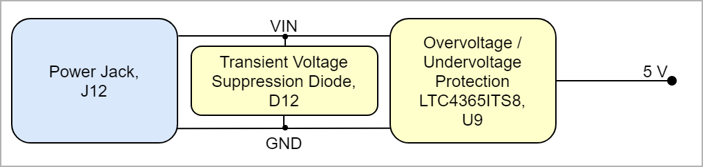
There is a transient voltage suppression diode (D12) which protects the board from voltage spikes. Additionaly, there is an overvoltage / undervoltage protection device (U9) for board protection.