...
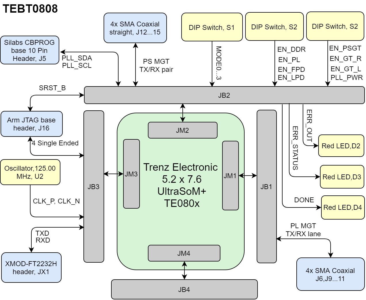
- Single 3.3V input (Direct modules power supply)
- Header for TE0790 JTAG/UART Adapter
- 20 Pin ARM JTAG header (connected to MIO JTAG 0)
- 10 Pin I2C header for Silabs Clock Builder Field Programmer
- Done, Error /and Status LEDs
- One PL GT with SMA connectors
- One PS GT with SMA connectors
- GT local loopback
- PL I/O loopbacks
- PS I/O loopbacks
- Boot Mode switches
- Power control switches to control TE080x power domains
- One pre-assembled TE0790 XMOD FTDI JTAG adapter
...
| Scroll Title |
|---|
| anchor | Figure_OV_BD |
|---|
| title | TEBT0808 block diagramBlock Diagram |
|---|
|
| Scroll Ignore |
|---|
| draw.io Diagram |
|---|
| border | false |
|---|
| viewerToolbar | true |
|---|
| |
|---|
| fitWindow | false |
|---|
| diagramDisplayName | |
|---|
| lbox | true |
|---|
| revision | 1213 |
|---|
| diagramName | TEBT0808_OV_BD |
|---|
| simpleViewer | false |
|---|
| width | |
|---|
| links | auto |
|---|
| tbstyle | hidden |
|---|
| diagramWidth | 640 |
|---|
|
|
| Scroll Only |
|---|
|
|
...
| Scroll Title |
|---|
| anchor | Figure_OV_BD |
|---|
| title | TEBT0808 main componentsMain Components |
|---|
|
| Scroll Ignore |
|---|
| draw.io Diagram |
|---|
| border | true |
|---|
| viewerToolbar | true |
|---|
| |
|---|
| fitWindow | false |
|---|
| diagramName | TEBT0808_OV_MC |
|---|
| simpleViewer | false |
|---|
| width | |
|---|
| diagramWidth | 640 |
|---|
| revision | 3 |
|---|
|
|
| Scroll Only |
|---|
|
|
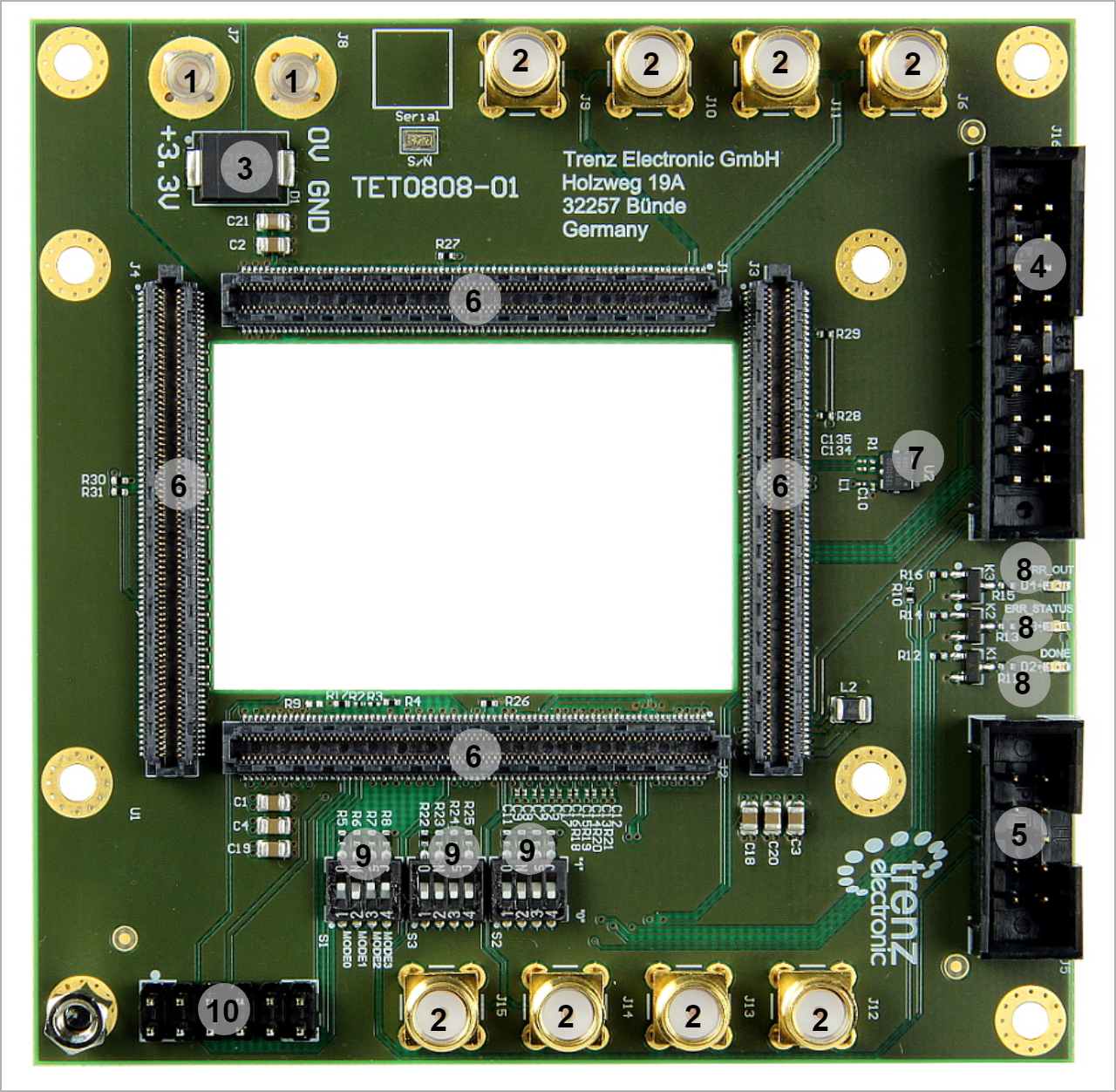
- Uninsulated 2 mm rigid socketNon-insulated Jack. J8-J7
- SMA Coaxial straight. J6- J9...15
- Surface Mount Schottky Barrier Rectifier. D1
- Box Headers, Straight/Angled J5-J16
- Board to Board Connector. J1...4
- Clock Oscillator, U2
- On-Board LED, D2...4
- DIP-Switch, S1...3
- XMOD JTAG Base, JX1
Initial Delivery State
| Page properties |
|---|
|
Notes : Only components like EEPROM, QSPI flash and DDR3 can be initialized by default at manufacture. If there is no components which might have initial data ( possible on carrier) you must keep the table empty |
...
| Scroll Title |
|---|
| anchor | Table_OV_BP |
|---|
| title | Boot processProcess. |
|---|
|
| Scroll Table Layout |
|---|
| orientation | portrait |
|---|
| sortDirection | ASC |
|---|
| repeatTableHeaders | default |
|---|
| style | |
|---|
| widths | |
|---|
| sortByColumn | 1 |
|---|
| sortEnabled | false |
|---|
| cellHighlighting | true |
|---|
|
| M3 | M2 | M1 | M0 | Bootmode Hex | Bootmode | Notes |
|---|
| ON | ON | ON | ON | 0x00xF | PS Main JTAG (TE0790 USB JTAG) |
| | ON | ON | OFF | ON | 0x20xD | SPI Flash (dual parallel, 4bit x 2, 32bit Addressing) |
| | ON | OFF | OFF | OFF | 0x8 | PJTAG(MIO29:26) |
|
|
...
| Scroll Title |
|---|
| anchor | Table_OV_RST |
|---|
| title | Reset processProcess. |
|---|
|
| Scroll Table Layout |
|---|
| orientation | portrait |
|---|
| sortDirection | ASC |
|---|
| repeatTableHeaders | default |
|---|
| style | |
|---|
| widths | |
|---|
| sortByColumn | 1 |
|---|
| sortEnabled | false |
|---|
| cellHighlighting | true |
|---|
|
Signal | B2B | Note |
|---|
PLL_RST | J2-89 |
| | SRST_B | J2-96 | connected Connected to PJTAG0_SRST - J16 |
|
Signals, Interfaces and Pins
...
| Scroll Title |
|---|
| anchor | Table_SIP_B2B |
|---|
| title | General PL I/O to B2B connectors information |
|---|
|
| Scroll Table Layout |
|---|
| orientation | portrait |
|---|
| sortDirection | ASC |
|---|
| repeatTableHeaders | default |
|---|
| style | |
|---|
| widths | |
|---|
| sortByColumn | 1 |
|---|
| sortEnabled | false |
|---|
| cellHighlighting | true |
|---|
|
| B2B Connector | Interfaces | Number of I/O | Notes |
|---|
J1
| User I/O | 22 singel endedSingle Ended, 11 Differential 8 singel endedSingle Ended, 4 Differential 8 singel endedSingle Ended, 4 Differential 8 singel endedSingle Ended, 4 Differential 3 singel endedSingle Ended | Connected to Bank 66 Connected to Bank 228 Connected to Bank 229 Connected to Bank 230 VCCO_66, PL_1V8 | J2
| Ethernet PHY | 32 singel endedSingle Ended, 16 Differential 4 singel endedSingle Ended, 16 Differential | Connected to Bank 505 Connected to Bank 128 | | Control Signals | 15 single endedSingle Ended | PLL_SEL0, PLL_SEL1, PLL_RST, EN_GTR, EN_PL, PLL_LOLN, EN_PSGT, ERR_STATUS, ERR_OUT,SRST_B, INIT_B, PROG_B, EN_FPD , EN_LPD , DONE | | Power Control Signal | 10 single endedSingle Ended | EN_PLL_PWR, PLL_FINC ,PG_PLL_1V8, LP_GOOD, PG_DDR, PG_PL, PG_FPD, PG_PSGT, PG_GT_R, PG_GT_L | | JTAG Interface | 7 single endedSingle Ended | TCK, TDI, TMS, TDO, MR, Rxd, Txd | | WANNE2 | 2 single endedSingle Ended | PLL_SCL, PLL_SDA | | Clock | 6 singel endedSingle Ended, 3 Differential | CLK0, CLK7, CLK8 | J3
| User I/O | 12 singel endedSingle Ended, 6 Differential 12 singel endedSingle Ended, 6 Differential | Connected to Bank 48 Connected to Bank 47 | | Clock | 6 singel endedSingle Ended, 3 Differential | CLK228, CLK229, CLK230 | | PJTAG Interface | 7 single endedSingle Ended | PJTAG0_TCK, PJTAG0_TDI, PJTAG0_TMS, PJTAG0_TDO, | | MIO | 27 single endedSingle Ended | MIO19..76 | | UART | 2 single endedSingle Ended | TXD, RXD | | Power pins | 4 single endedSingle Ended | PS_1V8, SI_PLL_1V8, VCCO_48, VCCO_47 | | J4 | User I/O | 48 singel endedSingle Ended, 62 Differential 4 single endedSingle Ended | Connected to Bank 64 Connected to Bank 64 | | Power pins | 4 single endedSingle Ended | VCCO_64, VCCO65 |
|
XMOD JTAG
JTAG access to the TE080x UltraSoM+ TEBT0808 is available through B2B connector JM2 .
TODO XMOD Pin Header and recommended XMOD DIP setting and used MIO on B2B connector
PJTAG
TODO Pin Header
TODO Pin Header
SMA
TODO Pin Header
Test Points
...
using XMOD JTAG adapter TE0790 adapter.
| Scroll Title |
|---|
| anchor | Table_SIP_JTG |
|---|
| title | JTAG Pins Connection |
|---|
|
| Scroll Table Layout |
|---|
| orientation | portrait |
|---|
| sortDirection | ASC |
|---|
| repeatTableHeaders | default |
|---|
| style | |
|---|
| widths | |
|---|
| sortByColumn | 1 |
|---|
| sortEnabled | false |
|---|
| cellHighlighting | true |
|---|
|
JTAG Signal | B2B Connector | Notes |
|---|
| TMS | J2- 126 |
| | TDI | J2- 122 |
| | TDO | J2- 124 |
| | TCK | J2- 120 |
|
|
There is a DIP switch on TE0790 adapter which must be set accordingly.
| Scroll Title |
|---|
| anchor | Table_SIP_Xmod_DIP |
|---|
| title | Xmod Adapter DIP-Switch Setting Description |
|---|
|
| Scroll Table Layout |
|---|
| orientation | portrait |
|---|
| sortDirection | ASC |
|---|
| repeatTableHeaders | default |
|---|
| style | |
|---|
| widths | |
|---|
| sortByColumn | 1 |
|---|
| sortEnabled | false |
|---|
| cellHighlighting | true |
|---|
|
| DIP Switch | ON | OFF | Default | Description |
|---|
| 1 | Normal mode | Adapter board CPLD update mode | ON | Update Mode JTAG access to SC CPLD only | | 2 | Do not use (illegal setting) | Normal mode | OFF | Must be always in OFF state. | | 3 | VIO connected to 3.3V | Power VIO from pin header J2 | OFF | User I/O Voltage | | 4 | Power 3.3V from USB | Power 3.3V from pin header J2 | OFF | Power on-board peripherals (FTDI chip & SC CPLD, ...) |
|
The voltages 3.3V (VCC) and VIO (variable SC CPLD I/O-voltage) can be configured by the DIP-switches 3 and 4:
| Scroll Title |
|---|
| anchor | Table_SIP_Xmod_DIP |
|---|
| title | Xmod Adapter DIP-Switch Setting Description |
|---|
|
| Scroll Table Layout |
|---|
| orientation | portrait |
|---|
| sortDirection | ASC |
|---|
| repeatTableHeaders | default |
|---|
| style | |
|---|
| widths | |
|---|
| sortByColumn | 1 |
|---|
| sortEnabled | false |
|---|
| cellHighlighting | true |
|---|
|
| DIP Switch-3 | DIP Switch-4 | 3.3V (VCC) Pin 5 | VIO Pin 6 | Description |
|---|
| OFF | OFF | 3.3V from base (input**) | VIO from base (input**) | 3.3V (pin 5) and VIO (pin 6) sourced from base | | OFF | ON | 3.3V from USB* (output**) | VIO from base (input**) | VIO sourced from base by Pin 6 | | ON | OFF | 3.3V from base (input**) | 3.3V from base (input**) | VIO and 3.3V source by base (Pin 5 and Pin 6 are shorted and both must be sourced by 3.3V) | | ON | ON | 3.3V from USB* (output**) | 3.3V from USB* (output**) | 3.3V (pin 5) and VIO (pin 6) sourced USB (Pin 5 and Pin 6 are shorted and both are 3.3V) |
|
PJTAG
PJTAG access to the TEBT0808 is available through B2B connector JM3.
| Scroll Title |
|---|
| anchor | Table_SIP_JTG |
|---|
| title | PJTAG Pins Connection |
|---|
|
| Scroll Table Layout |
|---|
| orientation | portrait |
|---|
| sortDirection | ASC |
|---|
| repeatTableHeaders | default |
|---|
| style | |
|---|
| widths | |
|---|
| sortByColumn | 1 |
|---|
| sortEnabled | false |
|---|
| cellHighlighting | true |
|---|
|
JTAG Signal | B2B Connector | Notes |
|---|
| TMS | J3- 94 |
| | TDI | J3- 90 |
| | TDO | J3- 92 |
| | TCK | J3- 88 |
| | SRST | J2- 96 | Connected to SRST_B |
|
I2C signals can be accessed through pin header J5.
| Scroll Title |
|---|
| anchor | Table_SIP_I2C |
|---|
| title | I2C Connections |
|---|
|
| Scroll Table Layout |
|---|
| orientation | portrait |
|---|
| sortDirection | ASC |
|---|
| repeatTableHeaders | default |
|---|
| style | |
|---|
| widths | |
|---|
| sortByColumn | 1 |
|---|
| sortEnabled | false |
|---|
| cellHighlighting | true |
|---|
|
Signals | B2B Connector | Pin Header | Notes |
|---|
| PLL_SCL | J2- 90 | J5- 3 |
| | PLL_SDA | J2- 92 | J5- 7 |
|
|
SMA Coaxial
| Scroll Title |
|---|
| anchor | Table_SIP_SMA |
|---|
| title | SMA Connections |
|---|
|
| Scroll Table Layout |
|---|
| orientation | portrait |
|---|
| sortDirection | ASC |
|---|
| repeatTableHeaders | default |
|---|
| style | |
|---|
| widths | |
|---|
| sortByColumn | 1 |
|---|
| sortEnabled | false |
|---|
| cellHighlighting | true |
|---|
|
Designator | Signals | B2B Connector | Notes |
|---|
| J6 | B230_TX3_P | J1-2 |
| | J9 | B230_RX3_N | J1-5 |
| | J10 | B230_RX3_P | J1-3 |
| | J11 | B230_TX3_N | J1-4 |
| | J12 | B505_TX0_N | J2-67 |
| | J13 | B505_TX0_P | J2-69 |
| | J14 | B505_RX0_N | J2-70 |
| | J15 | B505_RX0_P | J2-72 |
|
|
Test Points
| Scroll Title |
|---|
| anchor | Table_SIP_TestPoint |
|---|
| title | Test Points Information |
|---|
|
| Scroll Table Layout |
|---|
| orientation | portrait |
|---|
| sortDirection | ASC |
|---|
| repeatTableHeaders | default |
|---|
| style | |
|---|
| widths | |
|---|
| sortByColumn | 1 |
|---|
| sortEnabled | false |
|---|
| cellHighlighting | true |
|---|
|
Test Point | Signals | B2B Connector | Notes |
|---|
| 1 | DDR_1V2 | J2-135 |
| | 2 | PG_PSGT | J2-82 |
| | 3 | ERR_STATUS | J2-86 |
| | 4 | PLL_FDEC | J2-94 |
| | 5 | EN_LPD | J2-108 |
| | 6 | EN_DDR | J2-112 |
| | 7 | PG_PL | J2-104 |
| | 8 | PG_PLL_1V8 | J2-80 |
| | 9 | N_PSGT | J2-84 |
| | 10 | ERR_OUT | J2-88 |
| | 11 | EN_FPD | J2-102 |
| | 12 | LP_GOOD | J2-106 |
| | 13 | PG_FPD | J2-110 |
| | 14 | PG_DDR | J2-114 |
| | 15 | EN_PLL_PWR | J2-77 |
| | 16 | PLL_FINC | J2-81 |
| | 17 | PG_GT_R | J2-91 |
| | 18 | EN_GT_R | J2-95 |
| | 19 | EN_PL | J2-101 |
| | 20 | EN_GT_L | J2-79 |
| | 21 | PLL_SEL0 | J2-93 |
| | 22 | PG_GT_L | J2-97 |
| | 23 | INIT_B | J2-98 |
| | 24 | IN1_P | J2-4 |
| | 25 | PLL_SEL1 | J2-87 |
| | 26 | PLL_LOLN | J2-85 |
| | 27 | PLL_RST | J2-89 |
| | 28 | DX_P | J2-119 |
| | 29 | DX_N | J2-121 |
| | 30 | IN1_N | J2-6 |
| | 31 | B505_CLK0_P | J2-10 |
| | 32 | B505_CLK0_N | J2-12 |
| | 33 | B505_CLK1_P | J2-16 |
| | 34 | B505_CLK1_N | J2-18 |
| | 35 | B128_CLK1_P | J2-22 |
| | 36 | B128_CLK1_N | J2-24 |
| | 37 | CLK0_N | J2-1 |
| | 38 | CLK0_P | J2-3 |
| | 39 | CLK8_P | J2-7 |
| | 40 | CLK8_N | J2-9 |
| | 41 | CLK7_P | J2-13 |
| | 42 | CLK7_N | J2-15 |
| | 43 | IN2_P | J3-66 |
| | 44 | IN2_N | J3-68 |
| | 45 | B230_CLK1_N | J3-59 |
| | 46 | B230_CLK1_P | J3-61 |
| | 47 | B229_CLK0_N | J3-65 |
| | 48 | B229_CLK0_P | J3-67 |
| | 49 | PLL_3V3 | J3-152 |
| | 50 | GND | J3-155 |
| | 51 | PL_1V8 | J1-121 |
| | 52 | PS_1V8 | J3-147 |
| | 53 | SI_PLL_1V8 | J3-151 |
| | 54 | PROG_B | J2-100 |
| | 55...56 | GND | - |
|
|
On-board Peripherals
| Page properties |
|---|
|
Notes : - add subsection for every component which is important for design, for example:
- Two 100 Mbit Ethernet Transciever PHY
- USB PHY
- Programmable Clock Generator
- Oscillators
- eMMCs
- RTC
- FTDI
- ...
- DIP-Switches
- Buttons
- LEDs
|
...
| Scroll Title |
|---|
| anchor | Table_OBP |
|---|
| title | On board peripheralsBoard Peripherals |
|---|
|
| Scroll Table Layout |
|---|
| orientation | portrait |
|---|
| sortDirection | ASC |
|---|
| repeatTableHeaders | default |
|---|
| style | |
|---|
| widths | |
|---|
| sortByColumn | 1 |
|---|
| sortEnabled | false |
|---|
| cellHighlighting | true |
|---|
|
|
DIP Switch
...
Control signals must be set by using DIP Switch S2, S3.
| Scroll Title |
|---|
| anchor | Table_OBP_DIP |
|---|
| title | DIP Switch S2 |
|---|
|
| Scroll Table Layout |
|---|
| orientation | portrait |
|---|
| sortDirection | ASC |
|---|
| repeatTableHeaders | default |
|---|
| style | |
|---|
| widths | |
|---|
| sortByColumn | 1 |
|---|
| sortEnabled | false |
|---|
| cellHighlighting | true |
|---|
|
| Signals | B2B | S2 switch | Notes |
|---|
| EN_PSGT | J2-84 | S2A |
| | EN_GT_R | J2-95 | S2B |
| | EN_GT_L | J2-97 | S2C |
| | EN_PLL_PWR | J2-77 | S2D | connected to PG_PL |
|
...
| Scroll Title |
|---|
| anchor | Table_PWR_PR |
|---|
| title | Module power rails. |
|---|
|
| Scroll Table Layout |
|---|
| orientation | portrait |
|---|
| sortDirection | ASC |
|---|
| repeatTableHeaders | default |
|---|
| style | |
|---|
| widths | |
|---|
| sortByColumn | 1 |
|---|
| sortEnabled | false |
|---|
| cellHighlighting | true |
|---|
|
| Power Rail Name | B2B JM1 Pin | B2B JM2 Pin | B2B JM3 Pin | B2B JM4 Pin | Direction | Notes |
|---|
| 3.3V | 151,153,155,157,159 | 140,142,144,146154,156,158,160,
153,155,157,159 | 157,158,159,160 | - | Output | Carrier power supply to module power rails PL_DCDCIN. DCDCIN, LP_DCDC, GT_DCDC, PL_3V3V | VCCO_47 | - | - | 43, 44 | - | Output | Connected to 1.8 (SI_PLL_1V8) | | VCCO_48 | - | - | 15,16 | - | Output | Connected to 1.8 (SI_PLL_1V8) | | VCCO_64 | - | - | - | 58, 106 | Output | Connected to 1.8 (PL_1V8) | | VCCO_65 | - | - | - | 69, 105 | Output | Connected to 1.8 (PL_1V8) | | VCCO_66 | 90,120 | - | - | - | Output | Connected to 1.8 (PL_1V8) | | PS_1V8 | - | 99, | 147, 148 | - | Input |
| | PLL_3V3 | - | - | 152 | - | Output | 3.3V | | PL_1_V8 | 121,121 | - | - | - | Input | 1.8V for PL Banks | | SI_PLL_1V8 | - | - | 151 | - | Input |
| | DDR 1V2 | - | 135 | - | - | Inout |
| | PL_3V3 | - | - | 152 | - | Output | Connected to 3.3V | | PSBAT | - | 125 | - | - | Output | 1.2V..1.5V, abs. max 2V |
|
...
| Scroll Title |
|---|
| anchor | Table_TS_ROC |
|---|
| title | Recommended operating conditions. |
|---|
|
| Scroll Table Layout |
|---|
| orientation | portrait |
|---|
| sortDirection | ASC |
|---|
| repeatTableHeaders | default |
|---|
| style | |
|---|
| widths | |
|---|
| sortByColumn | 1 |
|---|
| sortEnabled | false |
|---|
| cellHighlighting | true |
|---|
|
| Symbols | Min | Max | Unit | Note |
|---|
| VIN | 3,14 | 3.47 | V | Important, check also TRM of the connected module | | Operating Temperatur |
|
|
|
|
|
Physical Dimensions
Module size: 90 mm × 90 mm. Please download the assembly diagram for exact numbers.
Mating height with standard connectors: 3.5 mm.
...