Versions Compared

Key

  • This line was added.
  • This line was removed.
  • Formatting was changed.

...

Scroll Title
anchorFigure_OV_BD
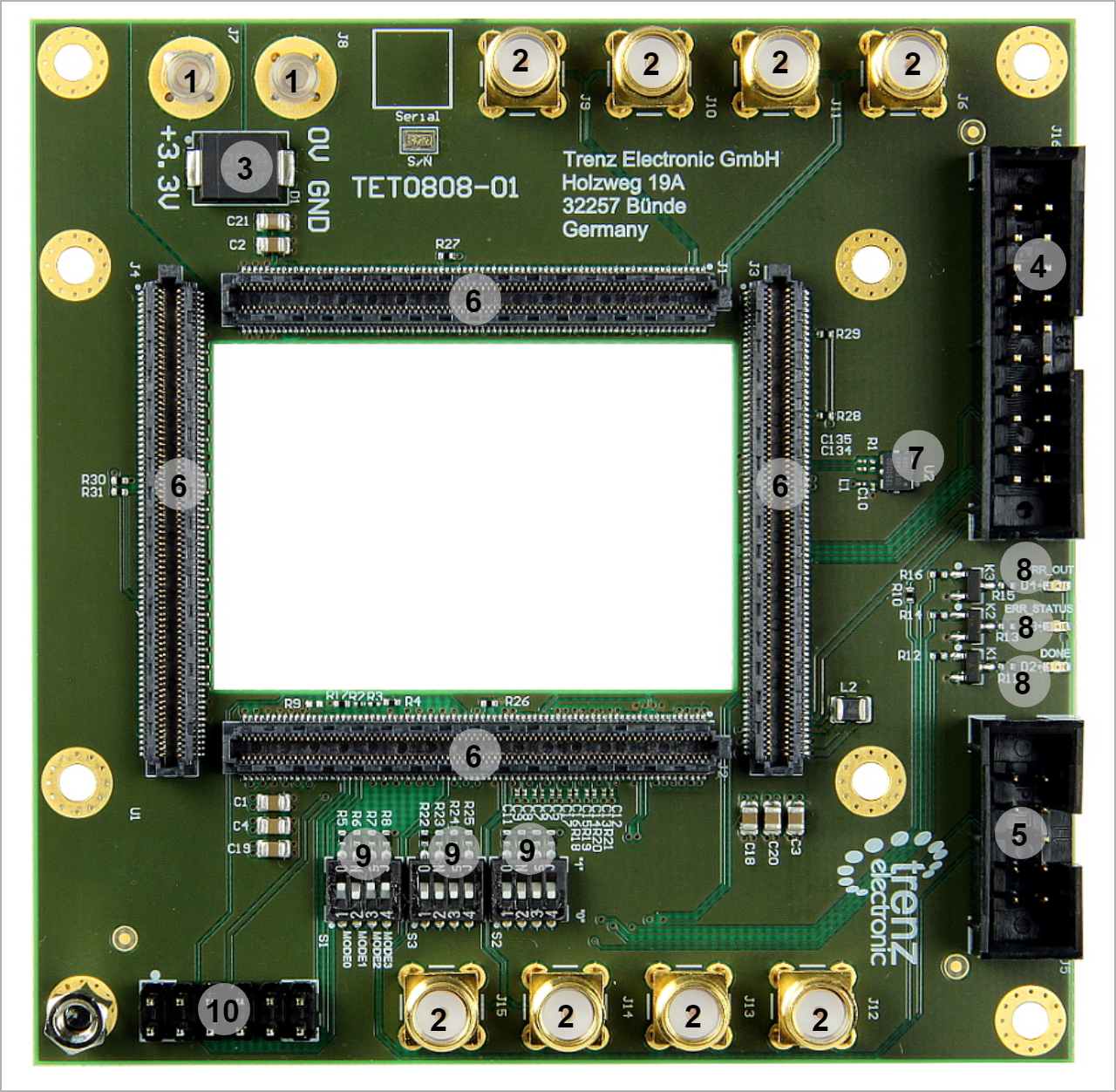
titleTEBT0808 Main Components


Scroll Ignore

draw.io Diagram
borderfalse
viewerToolbartrue
fitWindowfalse
diagramDisplayName
lboxtrue
revision34
diagramNameTEBT0808_OV_MC
simpleViewerfalse
width
linksauto
tbstylehidden
diagramWidth640


Scroll Only


  1. Non-insulated Power Jack. J8-J7
  2. SMA Coaxial straight. J6- J9...15
  3. Surface Mount Schottky Barrier Rectifier. D1
  4. ARM PJTAG Pin Header J16
  5. I2C Pin Header, J5Box Headers, Straight/Angled J5-J16
  6. Board to Board ConnectorConnectors. J1...4
  7. Clock MEMS Oscillator, U2
  8. On-Board LEDs, D2...4
  9. DIP-Switch, S1...3
  10. XMOD JTAG Base, JX1

...

Scroll Title
anchorTable_SIP_B2B
titleGeneral PL I/O to B2B connectors information

Scroll Table Layout
orientationportrait
sortDirectionASC
repeatTableHeadersdefault
style
widths
sortByColumn1
sortEnabledfalse
cellHighlightingtrue

B2B ConnectorInterfacesNumber of I/ONotes
J1

User I/O

22 Single Ended, 11 Differential

8 Single Ended, 4 Differential

8 Single Ended, 4 Differential

8 Single Ended, 4 Differential

3 Single Ended

Connected to Module FPGA, Bank 66

Connected to Module FPGA, Bank 228

Connected to Module FPGA, Bank 229

Connected to Module FPGA, Bank 230

VCCO_66, PL_1V8

J2

Ethernet PHY

32 Single Ended, 16 Differential

4 Single Ended, 16 Differential

Connected to to  Module FPGA, Bank 505

Connected to Module FPGA, Bank 128

Control Signals15 Single EndedPLL_SEL0, PLL_SEL1, PLL_RST, EN_GTR, EN_PL, PLL_LOLN, EN_PSGT, ERR_STATUS, ERR_OUT,SRST_B, INIT_B, PROG_B, EN_FPD , EN_LPD , DONE
Power Control Signal10 Single EndedEN_PLL_PWR, PLL_FINC ,PG_PLL_1V8, LP_GOOD, PG_DDR, PG_PL, PG_FPD, PG_PSGT, PG_GT_R, PG_GT_L
JTAG Interface7 Single EndedTCK, TDI, TMS, TDO, MR, Rxd, Txd
WANNE22 Single EndedPLL_SCL, PLL_SDA
Clock

6 Single Ended, 3 Differential

CLK0, CLK7, CLK8

J3


User I/O

12 Single Ended, 6 Differential

12 Single Ended, 6 Differential

Connected to Module FPGA, Bank 48

Connected to Module FPGA, Bank 47

Clock6 Single Ended, 3 DifferentialCLK228, CLK229, CLK230
PJTAG Interface7 Single EndedPJTAG0_TCK, PJTAG0_TDI, PJTAG0_TMS, PJTAG0_TDO,
MIO27 Single EndedMIO19..76
UART2 Single EndedTXD, RXD
Power pins4 Single EndedPS_1V8, SI_PLL_1V8, VCCO_48, VCCO_47
J4User I/O

48 Single Ended, 62 Differential

4 Single Ended

Connected to Module FPGA, Bank 64

Connected to Module FPGA, Bank 64

Power pins4 Single EndedVCCO_64, VCCO65


...

Scroll Title
anchorTable_SIP_Xmod_DIP
title Xmod Adapter DIP-Switch Setting Description

Scroll Table Layout
orientationportrait
sortDirectionASC
repeatTableHeadersdefault
style
widths
sortByColumn1
sortEnabledfalse
cellHighlightingtrue

DIP Switch-3DIP Switch-43.3V (VCC) Pin 5VIO Pin 6Description
OFFOFF3.3V from base (input)base VIO from base (input)3.3V (pin 5) and VIO (pin 6) sourced from base
OFFON3.3V from USB* (output)VIO from base (input)VIO sourced from base by Pin 6
ONOFF3.3V from base (input)3.3V from base (input)VIO and 3.3V source by base (Pin 5 and Pin 6 are shorted and both must be sourced by 3.3V)
ONON3.3V from USB (output)3.3V from USB* (output)

3.3V (pin 5) and VIO (pin 6) sourced USB (Pin 5 and Pin 6 are shorted and both are 3.3V)


...

Scroll Title
anchorTable_OBP_LED
titleOn-board LEDs

Scroll Table Layout
orientationportrait
sortDirectionASC
repeatTableHeadersdefault
style
widths
sortByColumn1
sortEnabledfalse
cellHighlightingtrue

DesignatorColorConnected toActive LevelNote
D2RedDONEActive
Low
HighNon User LED
D3RedERR_STATUSActive
Low
HighNon User LED
D4RedERR_OUTActive
Low
HighNon User LED


Clock Sources

Scroll Title
anchorTable_OBP_CLK
titleOsillators

Scroll Table Layout
orientationportrait
sortDirectionASC
repeatTableHeadersdefault
style
widths
sortByColumn1
sortEnabledfalse
cellHighlightingtrue

DesignatorDescriptionFrequencyNote
U2MEMS Oscillator125.00 MHz


...

Scroll Title
anchorFigure_PWR_PD
titlePower Distribution


Scroll Ignore

draw.io Diagram
borderfalse
viewerToolbartrue
fitWindowfalse
diagramDisplayName
lboxtrue
revision24
diagramNameTEBT0808_PWR_PD
simpleViewerfalse
width
linksauto
tbstylehidden
diagramWidth640


Scroll Only


...

Scroll Title
anchorTable_TS_AMR
titlePS absolute maximum ratings

Scroll Table Layout
orientationportrait
sortDirectionASC
repeatTableHeadersdefault
style
widths
sortByColumn1
sortEnabledfalse
cellHighlightingtrue

SymbolsMinMaxUnitNote
VIN-0.34V

VIN is connected directly to module

Storage Temperatur-40+85120°C


Recommended Operating Conditions

...

Scroll Title
anchorTable_TS_ROC
titleRecommended operating conditions.

Scroll Table Layout
orientationportrait
sortDirectionASC
repeatTableHeadersdefault
style
widths
sortByColumn1
sortEnabledfalse
cellHighlightingtrue

SymbolsMinMaxUnitNote
VIN3,143.47VImportant, check also TRM of the connected module
Operating Temperatur-40+85


Physical Dimensions

  • Module size: 90 mm × 90 mm.  Please download the assembly diagram for exact numbers.

  • Mating height with standard connectors: 3.5 mm.

...

Scroll Title
anchorTable_RH_HRH
titleHardware Revision History

Scroll Table Layout
orientationportrait
sortDirectionASC
repeatTableHeadersdefault
style
widths
sortByColumn1
sortEnabledfalse
cellHighlightingtrue

DateRevisionChangesDocumentation Link
2016-ß605-293001-Initial ReleaseREV01


Document Change History

Page properties
hiddentrue
idComments
  • Note this list must be only updated, if the document is online on public doc!
  • It's semi automatically, so do following
    • Add new row below first

    • Copy "Page Information Macro(date)" Macro-Preview, Metadata Version number, Author Name and description to the empty row. Important Revision number must be the same as the Wiki document revision number Update Metadata = "Page Information Macro (current-version)" Preview+1 and add Author and change description. --> this point is will be deleted on newer pdf export template

    • Metadata is only used of compatibility of older exports

...