...
| Page properties |
|---|
|
Important General Note:
|
...
| Page properties |
|---|
|
Note for Download Link of the Scroll ignore macro: |
| Scroll pdf ignore |
|---|
Table of Contents |
...
The Trenz Electronic TE0802 is an evalution modulea development board integrating a Xilinx Zynq UltraScale+ . Other assembly options for the FPGA and the memory chips are available. Please contact us for further information.
Refer to http://trenz.org/te0802-info for the current online version of this manual and other available documentation.
...
| Page properties |
|---|
|
Note:
'Key Features' description: Important components and connector or other Features of the module
→ please sort and indicate assembly options |
- MPSoC: Xilinx Zynq XCZU2CG -1SBVA484E
- SDRAM: LPDDR4-3733 8Gb 256Mx32
- Xilinx Zynq UltraScale+ MPSoC
- RAM/Storages:
- SDRAM: LPDDR4 8Gb 256Mx16x 2
- SPI
Storages:- SPI Flash 256Mb (32M x 8) 133MHz
- microSD Card
- M.2 SSD PCIe
- 133 MHz
- EEPROMs 2Kb (256 x 8)
- EEPROMs 4Kb (512 x 8)
- Display Interfaces:
- DisplayPort
- VGA
- 4 Digit 7-Segment LED Display
- 8 LEDs
- Audio:
- USB JTAG/UART microUSB
- 1GB Ethernet RJ45
- USB 3.0 Host (Type A Connector)
- microSD Card
- M.2 SSD PCIe
- 3.5 mm Earphone Jack (PWM Output)
- Display Port
- VGA
- 4 Digit 7-Segment LED Display
- 8 LEDs
Input:- 5 User Buttons
- 8 Bit Slide Switches
- Reset Button
User I/O:Communication:
- 1GB Ethernet RJ45
- USB 3.0 Host (Type A Connector)
- Debug
- Power
- Dimension: 100mm x 100mm
Block Diagram
| Page properties |
|---|
|
add drawIO object here.
|
...
| Scroll Title |
|---|
| anchor | Figure_OV_BD |
|---|
| title | TE0802 Block Diagram |
|---|
|
| Scroll Ignore |
|---|
| draw.io Diagram |
|---|
| border | truefalse |
|---|
| viewerToolbar | true |
|---|
| |
|---|
| fitWindow | false |
|---|
| diagramDisplayName | |
|---|
| lbox | true |
|---|
| revision | 4 |
|---|
| diagramName | TE0802 | diagramName | TE08202-02_OV_BD |
|---|
| simpleViewer | false |
|---|
| width | |
|---|
| links | auto |
|---|
| diagramWidthtbstyle | 611hidden |
|---|
| revisiondiagramWidth | 13638 |
|---|
|
|
| Scroll Only |
|---|
 Image Removed Image Removed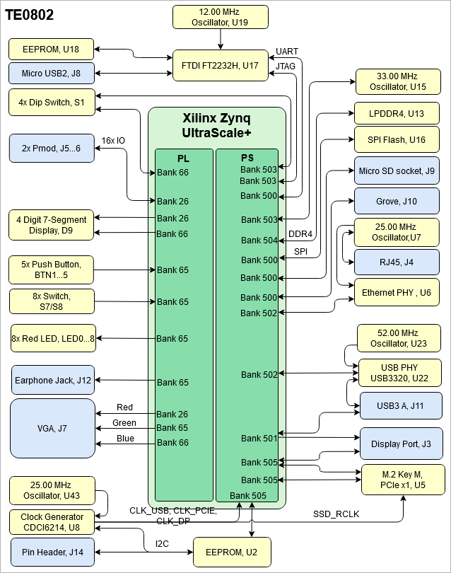 Image Added Image Added
|
|
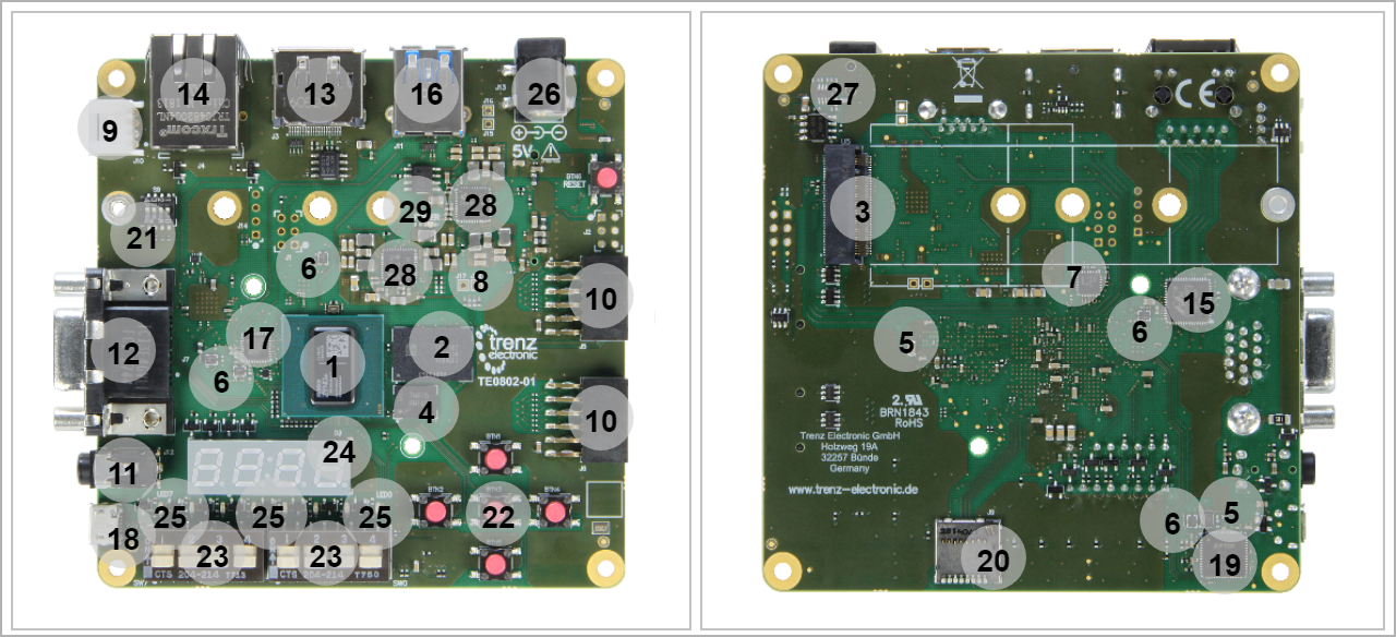
Main Components
| Page properties |
|---|
|
Notes : - Picture of the PCB (top and bottom side) with labels of important components
- Add List below
|
...
| Scroll Title |
|---|
| anchor | Figure_OV_MC |
|---|
| title | TE0802 Main Components (Picture shows Revision 01) |
|---|
|
| Scroll Ignore |
|---|
| draw.io Diagram |
|---|
| border | truefalse |
|---|
| viewerToolbar | true |
|---|
| |
|---|
| fitWindow | false |
|---|
| diagramDisplayName | |
|---|
| lbox | true |
|---|
| revision | 10 |
|---|
| diagramName | TE0802_OV_MC |
|---|
| simpleViewer | falsetrue |
|---|
| width | |
|---|
| links | auto |
|---|
| diagramWidthtbstyle | 602hidden |
|---|
| revisiondiagramWidth | 8640 |
|---|
|
|
| Scroll Only |
|---|
|
|
- Xilinx Zynq UltraScale+ MPSoc, U14
- LPDDR4 SDRAM, U13
- M.2 Key M PCIe x1, U5
- SPI Flash Memory, U16
- EEPROM, U2, U18
- Oscillator, U15, U7, U19, U23, U43
- Clock Generator, U8
- Clock Generator Programming Connector, J14
- Grove Connector, J10
- Pmod Host Socket, J5...6
- Headphone Jack, J12
- D-Sub Connector, J7
- DisplayPort, J3
- RJ45 Socket, J4
- Ethernet PHY, U6
- USB Type A, J11
- USB 2.0 PHY, U22
- Micro USB 2.0 Type B, J8
- FTDI USB 2.0 to JTAG/UART Converter, U17
- microSD Card, J9
- Slide Switch, S1
- Push Button, BTN1...5
- DIP Switch, S7...8
- 4 Digit 7-Segment LED Display, D9
- 8x LEDs (Red), LED0...7
- Power Jack, J13
- Overvoltage/Undervoltage/Reverse Supply Protector, U12
- Power Management Integrated Circuit (PMIC), U1, U9
- Power Good LED (Green), D12
...
| Scroll Title |
|---|
| anchor | Table_OV_IDS |
|---|
| title | Initial Delivery State of Programmable Devices on the Module |
|---|
|
| Scroll Table Layout |
|---|
| orientation | portrait |
|---|
| sortDirection | ASC |
|---|
| repeatTableHeaders | default | style |
|---|
| widths | sortByColumn | 1 |
|---|
| sortEnabled | false |
|---|
| cellHighlighting | true |
|---|
|
Storage device name | Content | Notes |
|---|
SPI Flash (U16) | Not programmed |
| | EEPROM (U2) | Not programmed | Except Ethernet MAC | | EEPROM (U18) | Programmed | FTDI Configuration | | LPDDR4 SDRAM (U13) | Not programmed |
|
|
Configuration Signals
| Page properties |
|---|
|
- Overview of Boot Mode, Reset, Enables.
|
Bootmode signals must be set through DIP Switch S1.
| Scroll Title |
|---|
| anchor | Table_OV_BP |
|---|
| title | Boot process.Process |
|---|
|
| Scroll Table Layout |
|---|
| orientation | portrait |
|---|
| sortDirection | ASC |
|---|
| repeatTableHeaders | default | style | widths |
|---|
| sortByColumn | 1 |
|---|
| sortEnabled | false |
|---|
| cellHighlighting | true |
|---|
|
|
| Scroll Title |
|---|
| anchor | Table_OV_RST |
|---|
| title | Reset process. |
|---|
|
| Scroll Table Layout |
|---|
| orientation | portrait |
|---|
| sortDirection | ASC |
|---|
| repeatTableHeaders | default |
|---|
style | widths | | sortByColumn | 1 |
|---|
| sortEnabled | false |
|---|
| cellHighlighting | true |
|---|
Signal | B2B | I/O | Note |
|---|
S1-2(B) | MODE0 S1-1(A) | Boot Mode |
|---|
MODE[2:0]=000 | OFF | OFF | JTAG | MODE[2:0]=001 | OFF | ON | not supported | MODE[2:0]=010 | ON | OFF | QSPI(32 bit) | MODE[2:0]=011 | ON | ON | SD0(2.0) |
|
Reset setting is available through Push Button BTN6.
| Scroll Title |
|---|
| anchor | Table_OV_RST |
|---|
| title | Reset Process |
|---|
|
| Scroll Table Layout |
|---|
| orientation | portrait |
|---|
| sortDirection | ASC |
|---|
| repeatTableHeaders | default |
|---|
| sortByColumn | 1 |
|---|
| sortEnabled | false |
|---|
| cellHighlighting | true |
|---|
|
Signal | Connected to | Note |
|---|
POR_B | BTN6, Push Button | Connected to nRESET |
|
Signals, Interfaces and Pins
| Page properties |
|---|
|
Notes : - For carrier or stand-alone boards use subsection for every connector type (add designator on description, not on the subsection title), for example:
- For modules which needs carrier use only classes and refer to B2B connector if more than one is used, for example
|
JTAG Interface
I/Os on Pin Headers and Connectors
FPGA bank number and number of I/O signals connected to the connectors:JTAG access to the TExxxx SoM through B2B connector JMX.
| Scroll Title |
|---|
| anchor | Table_SIP_JTGB2B |
|---|
| title | JTAG pins connectionGeneral I/O to Pin Header and Connectors Information |
|---|
|
| Scroll Table Layout |
|---|
| orientation | portrait |
|---|
| sortDirection | ASC |
|---|
| repeatTableHeaders | default | style | widths |
|---|
| sortByColumn | 1 |
|---|
| sortEnabled | false |
|---|
| cellHighlighting | true |
|---|
|
|
JTAG Signal | B2B Connector |
|---|
TMS | TDI | TDO | TCK | JTAG_EN |
MIO Pins
...
you must fill the table below with group of MIOs which are connected to a specific components or peripherals, you do not have to specify pins in B2B, Just mention which B2B is connected to MIOs. The rest is clear in the Schematic.
Example:
| FPGA Bank | Connector | I/O Signal Count | Voltage Level | Notes |
|---|
| Bank 503 | Micro USB, J8 (over FTDI) | 4 Single Ended | 3.3 V | JTAG | | Bank 500 | Micro USB, J8 (over FTDI) | 2 Single Ended | 3.3 V | UART | | Bank 500 | Micro SD Card, J9 | 7 Single Ended | 3.3 V |
| | Bank 502 | ETH RJ45, J4 (over ETH PHY) | 14 Single Ended | 1.8 V |
| | Bank 505, 502 | USB 3.0, J11 (USB2 over USB PHY) | 2 Differential Pairs, 12 Single Ended | -- / 1.8V |
| Bank 505, 501 | SSD M.2, U5 | 2 Differential Pairs, 5 Single Ended | -- / 3.3 V |
| | Bank 505, 501 | Display Port Connector, J3 | 2 Differential Pairs, 5 Single Ended | --/ 3.3 V |
| | Bank 26, 65, 66, | D-Sub Host Socket (VGA), J7 | 14 Single Ended | 3.3 V / 1.8 V / 1.8 V |
| | Bank 65 | Earphone, J12 | 3 Single Ended | 1.8 V |
| | Bank 500 | Grove Connector, J10 | 2 Single Ended | 3.3 V |
| | Bank 26 | Pmod Host Socket, J5 | 8 Single Ended | 3.3 V |
| | Bank 26 | Pmod Host Socket, J6 | 8 Single Ended | 3.3 V |
|
|
Micro SD Card
TE0802 is equipped with a micro SD card connector (J9).
| Scroll Title |
|---|
| anchor | Table_SIP_SD |
|---|
| title | Micro SD Card Connector Information |
|---|
|
| Scroll Table Layout |
|---|
| orientation | portrait |
|---|
| sortDirection | ASC |
|---|
| repeatTableHeaders | default |
|---|
| sortByColumn | 1 |
|---|
| sortEnabled | false |
|---|
| cellHighlighting | true |
|---|
|
| Schematic | Connected to | Notes |
|---|
| SD_DAT0 | MIO 13, FPGA Bank 500 |
| | SD_DAT1 | MIO 14, FPGA Bank 500 |
| | SD_DAT2 | MIO 15, FPGA Bank 500 |
| | SD_DAT3 | MIO 16, FPGA Bank 500 |
| | SD_CLK | MIO 22, FPGA Bank 500 |
| | SD_CMD | MIO 21, FPGA Bank 500 |
| | SD_CD | MIO 24, FPGA Bank 500 |
|
|
RJ45 Connector
TE0802 is equipped with a RJ45 connector and an Ethernet PHYs. RJ45 connector J4 is connected to Ethernet PHYs U6.
| Scroll Title |
|---|
| anchor | Table_SIP_RJ45 |
|---|
| title | RJ45 Connector Information |
|---|
|
| Scroll Table Layout |
|---|
| orientation | portrait |
|---|
| sortDirection | ASC |
|---|
| repeatTableHeaders | default |
|---|
|
|
...
SPI_CS , SPI_DQ0... SPI_DQ3
SPI_SCK
...
| anchor | Table_OBP_MIOs |
|---|
| title | MIOs pins |
|---|
...
| Page properties |
|---|
|
Notes : - add subsection for every component which is important for design, for example:
- Two 100 Mbit Ethernet Transciever PHY
- USB PHY
- Programmable Clock Generator
- Oscillators
- eMMCs
- RTC
- FTDI
- ...
- DIP-Switches
- Buttons
- LEDs
|
| Page properties |
|---|
|
Notes : In the on-board peripheral table "chip/Interface" must be linked to the corresponding chapter or subsection |
| Scroll Title |
|---|
| anchor | Table_OBP |
|---|
| title | On board peripherals |
|---|
|
| Scroll Table Layout |
|---|
| orientation | portrait |
|---|
| sortDirection | ASC |
|---|
| repeatTableHeaders | default |
|---|
| style | widths |
|---|
| sortByColumn | 1 |
|---|
| sortEnabled | false |
|---|
| cellHighlighting | true |
|---|
|
|
Quad SPI Flash Memory
| Page properties |
|---|
|
Notes : Minimum and Maximum density of quad SPI flash must be mentioned for other assembly options. |
...
| anchor | Table_OBP_SPI |
|---|
| title | Quad SPI interface MIOs and pins |
|---|
| 2 | PHY_MDI0_P | MDIP[0] |
| | 3 | PHY_MDI0_N | MDIN[0] |
| | 4 | PHY_MDI1_P | MDIP[1] |
| | 5 | PHY_MDI1_N | MDIN[1] |
| | 6 | PHY_MDI2_P | MDIP[2] |
| | 7 | PHY_MDI2_N | MDIN[2] |
| | 8 | PHY_MDI3_P | MDIP[3] |
| | 9 | PHY_MDI3_N | MDIN[3] |
|
|
USBs Sockets
TE0802 is equipped with a Micro USB2.0 B connector J8 and a USB3.0 connector J11.
FTDI FT2232 (U17) can be accessed through Micro USB 2.0 B connector (J8) for JTAG (channel A). Channel B is connected to the FPGA and can be used for UART.
| Scroll Title |
|---|
| anchor | Table_SIP_USB2 |
|---|
| title | USB2.0 B Socket Information |
|---|
|
|
...
| Scroll Title |
|---|
| anchor | Table_OBP_RTC |
|---|
| title | I2C interface MIOs and pins |
|---|
|
| Scroll Table Layout |
|---|
| orientation | portrait |
|---|
| sortDirection | ASC |
|---|
| repeatTableHeaders | default | style |
|---|
| widths | sortByColumn | 1 |
|---|
| sortEnabled | false |
|---|
| cellHighlighting | true |
|---|
|
MIO U? Pin| Connected to | Notes |
|---|
| D- | D_N | FTDI, U17 |
| | D+ | D_P | FTDI, U17 |
| | Vbus | USB_VBUS | GND |
|
|
| Scroll Title |
|---|
| anchor | Table_OBPSIP_I2C_RTCUSB3 |
|---|
| title | I2C Address for RTCUSB3.0 A Socket Information |
|---|
|
scroll| Scroll Table Layout |
|---|
| orientation | portrait |
|---|
| sortDirection | ASC |
|---|
| repeatTableHeaders | default | style | widths |
|---|
| sortByColumn | 1 |
|---|
| sortEnabled | false |
|---|
| cellHighlighting | true |
|---|
|
MIO I2C AddressDesignator |
...
|
title | anchor | Table | OBP | EEP
|---|
| title | I2C EEPROM interface MIOs and pins |
|---|
| Scroll Table Layout |
|---|
| orientation | portrait |
|---|
| sortDirection | ASC |
|---|
| repeatTableHeaders | default |
|---|
style | widths | | sortByColumn | 1 |
|---|
| sortEnabled | false |
|---|
| cellHighlighting | true |
|---|
MIO Pin | Schematic | U?? Pin | Notes| N | USB PHY, U22 |
| | D+ | USB0_D_P | USB PHY, U22 |
| | StdA_SSRX- | USB_RX2_N | FPGA Bank 505 |
| | StdA_SSRX+ | USB_RX2_P | FPGA Bank 505 |
| | StdA_SSTX- | USB_TX2_N | FPGA Bank 505 |
| | StdA_SSTX+ | USB_TX2_P | FPGA Bank 505 |
| | VBUS | VBUS | USB PHY, U22 |
|
|
SSD M.2 Connector
TE0802 is equipped with a SSD M.2 connector (U5).
| Scroll Title |
|---|
| anchor | Table_OBPSIP_I2C_EEPROMSSD |
|---|
| title | I2C address for EEPROMSSD M.2 Connector Information |
|---|
|
| Scroll Table Layout |
|---|
| orientation | portrait |
|---|
| sortDirection | ASC |
|---|
| repeatTableHeaders | default | style |
|---|
| widths | sortByColumn | 1 |
|---|
| sortEnabled | false |
|---|
| cellHighlighting | true |
|---|
|
MIO I2C AddressDesignator |
LEDs
...
| anchor | Table_OBP_LED |
|---|
| title | On-board LEDs |
|---|
| PERn0/SATA-B+ | SSD_RX3_N | Pin M22, FPGA Bank 505 |
| | PERp0/SATA-B- | SSD_RX3_P | Pin M21, FPGA Bank 505 |
| | PERn0/SATA-A+ | SSD_TXC3_N | Pin K22, FPGA Bank 505 |
| | PERp0/SATA-A- | SSD_TXC3_P | Pin M21, FPGA Bank 505 |
| | REFCLKN | SSD_RCLK_N | Pin 9, Clock Generator U8 |
| | REFCLKP | SSD_RCLK_P | Pin 10, Clock Generator U8 |
| | DAS/DSS# | SSD_DAS | MIO35, FPGA Bank 501 |
| | DEVSLP | SSD_SLEEP | MIO32, FPGA Bank 501 |
| | PERST# | SSD_PERSTn | MIO31, FPGA Bank 501 |
| | CLKREQ# | SSD_CLKRQ | MIO33, FPGA Bank 501 |
| | PEWake# | SSD_WAKE | MIO34, FPGA Bank 501 |
|
|
Display Port Connector
TE0802 is equipped with a Display Port connector (J3).
| Scroll Title |
|---|
| anchor | Table_SIP_DP |
|---|
| title | Display Port Socket Information |
|---|
|
| Scroll Table Layout |
|---|
| orientation | portrait |
|---|
| sortDirection | ASC |
|---|
| repeatTableHeaders | default |
|---|
| sortByColumn | 1 |
|---|
| sortEnabled | false |
|---|
| cellHighlighting | true |
|---|
|
| Schematic | Corresponding Signals | Connected to | Notes |
|---|
| DP_TX_L0_P/N | DP0_TX_P/N | Pin A19/A20, FPGA Bank 505 |
| | DP_TX_L1_P/N | DP1_TX_P/N | Pin C19/C20, FPGA Bank 505 |
| | DP_TX_AUX_P/N | DP_AUX_TX/RX | MIO27, MIO30, FPGA Bank 501 |
|
|
D-Sub Connector
TE0802 is equipped with a D-Sub connector (J7).
| Scroll Title |
|---|
| anchor | Table_SIP_VGA |
|---|
| title | D-Sub Connector Information |
|---|
|
| Scroll Table Layout |
|---|
| orientation | portrait |
|---|
| sortDirection | ASC |
|---|
| repeatTableHeaders | default |
|---|
| sortByColumn | 1 |
|---|
| sortEnabled | false |
|---|
| cellHighlighting | true |
|---|
|
| Schematic | Corresponding Signals | Connected to | Notes |
|---|
| VGA_RED | VGA_R0...3 | Bank 65 | Red Channel | | VGA_GREEN | VGA_G0...3 | Bank 65 | Green Channel | | VGA_BLUE | VGA_B0...3 | Bank 66 | Blue Channel | | VGA_RGB_HSYNC | VGA_HS | Bank 26 | Horizontal Sync | | VGA_RGB_VSYNC | VGA_VS | Bank 26 | Vertical Sync |
|
Headphone Connector
TE0802 is equipped with a headphone connector (J12).
| Scroll Title |
|---|
| anchor | Table_SIP_HP |
|---|
| title | Headphone Connector Information |
|---|
|
| Scroll Table Layout |
|---|
| orientation | portrait |
|---|
| sortDirection | ASC |
|---|
| repeatTableHeaders | default |
|---|
| sortByColumn | 1 |
|---|
| sortEnabled | false |
|---|
| cellHighlighting | true |
|---|
|
| Schematic | Connected to | Notes |
|---|
| JACKSNS | Pin F3, FPGA Bank 65 |
| | PWM_R | Pin F4, FPGA Bank 65 |
| | PWM_L | Pin E3, FPGA Bank 65 |
|
|
Grove Connector
TE0802 is equipped with a grove connector (J10).
| Scroll Title |
|---|
| anchor | Table_SIP_Grove |
|---|
| title | Grove Connector Information |
|---|
|
| Scroll Table Layout |
|---|
| orientation | portrait |
|---|
| sortDirection | ASC |
|---|
| repeatTableHeaders | default |
|---|
| sortByColumn | 1 |
|---|
| sortEnabled | false |
|---|
| cellHighlighting | true |
|---|
|
| Schematic | Connected to | Notes |
|---|
| Grove_SCL0 | MIO18, FPGA Bank 500 |
| | Grove_SDA0 | MIO19, FPGA Bank 500 |
|
|
Pmod Sockets
TE0802 has 2 Pmod 2x6 host sockets which are connected to the FPGA.
| Scroll Title |
|---|
| anchor | Table_SIP_PMOD |
|---|
| title | Pmod SMD Host Socket Information |
|---|
|
| Scroll Table Layout |
|---|
| orientation | portrait |
|---|
| sortDirection | ASC |
|---|
| repeatTableHeaders | default |
|---|
| sortByColumn | 1 |
|---|
| sortEnabled | false |
|---|
| cellHighlighting | true |
|---|
|
| Designator | Signals | Connected to | Notes |
|---|
| J5 | PMOD_A0...7 | Bank 26 |
| | J6 | PMOD_B0...7 | Bank 26 |
|
|
Test Points
| Scroll Title |
|---|
| anchor | Table_SIP_TestPoint |
|---|
| title | Test Points Information |
|---|
|
| Scroll Table Layout |
|---|
| orientation | portrait |
|---|
| sortDirection | ASC |
|---|
| repeatTableHeaders | default |
|---|
| style | |
|---|
| widths | |
|---|
| sortByColumn | 1 |
|---|
| sortEnabled | false |
|---|
| cellHighlighting | true |
|---|
|
Test Point | Signals | Notes |
|---|
| TP1 | +1.1V_LPDDR4 |
| | TP2 | +1.8V_MGTRAVTT |
| | TP3 | +1.8V_PL |
| | TP4 | FT_B_TX |
| | TP5 | DP_TX_PWR |
| | TP6 | GND |
| | TP7 | GND |
| | TP8 | PMIC2_SDA |
| | TP9 | PMIC2_TP |
| | TP10 | ONKEY2 |
| | TP11 | PMIC2_SCL |
| | TP12 | DP_TX_HPD |
| | TP13 | DP_TX_PWR |
| | TP14 | INT_SCL1 |
| | TP15 | INT_SDA1 |
| | TP16 | FT_B_RX |
| | TP17 | CLOCKDIST_OE |
| | TP18 | +0.85V_VCCINT |
| | TP19 | +3.3V |
| | TP20 | +1.8V_PS |
| | TP21 | ERR_STATUS |
| | TP22 | +1.2V_PSPLL |
| | TP23 | GND |
| | TP24 | GND |
| | TP25 | PMIC1_SCA |
| | TP26 | PMIC1_SDA |
| | TP27 | ONKEY1 |
| | TP28 | PMIC1_TP |
| | TP29 | POR_B |
| | TP30 | PSBATT |
| | TP31 | SRST_B |
| | TP32 | DONE |
| | TP33 | INIT_B |
| | TP34 | VBUS |
| | TP35 | USB_VBUS |
| | TP36 | PROG_B |
| | TP37 | ERR_OUT |
|
|
On-board Peripherals
| Page properties |
|---|
|
Notes : - add subsection for every component which is important for design, for example:
- Two 100 Mbit Ethernet Transciever PHY
- USB PHY
- Programmable Clock Generator
- Oscillators
- eMMCs
- RTC
- FTDI
- ...
- DIP-Switches
- Buttons
- LEDs
|
| Page properties |
|---|
|
Notes : In the on-board peripheral table "chip/Interface" must be linked to the corresponding chapter or subsection |
| Scroll Title |
|---|
| anchor | Table_OBP |
|---|
| title | On-board Peripherals |
|---|
|
| Scroll Table Layout |
|---|
| orientation | portrait |
|---|
| sortDirection | ASC |
|---|
| repeatTableHeaders | default |
|---|
| sortByColumn | 1 |
|---|
| sortEnabled | false |
|---|
| cellHighlighting | true |
|---|
|
|
Quad SPI Flash Memory
| Page properties |
|---|
|
Notes : Minimum and Maximum density of quad SPI flash must be mentioned for other assembly options. |
he TE0802 evaluation board has one single QSPI flash connected as x4. Flash size depends on the assembly option, default 32MB
| Scroll Title |
|---|
| anchor | Table_OBP_SPI |
|---|
| title | Quad SPI Interface MIOs and Pins |
|---|
|
| Scroll Table Layout |
|---|
| orientation | portrait |
|---|
| sortDirection | ASC |
|---|
| repeatTableHeaders | default |
|---|
| sortByColumn | 1 |
|---|
| sortEnabled | false |
|---|
| cellHighlighting | true |
|---|
|
| MIO Pin | Schematic | U16 Pin | Notes |
|---|
| MIO0 | MIO0 | B2 | SPI_CLK | | MIO1 | MIO1 | D2 | SPI_DQ1 | | MIO2 | MIO2 | C4 | SPI_DQ2 | | MIO3 | MIO3 | D4 | SPI_DQ3 | | MIO4 | MIO4 | D3 | SPI_DQ0 | | MIO5 | MIO5 | C2 | SPI_CS |
|
LPDDR4 SDRAM
| Page properties |
|---|
|
Notes : Minimum and Maximum density of DDR3 SDRAM must be mentioned for other assembly options. (pay attention to supported address length for DDR3) |
The TE0802 evaluation board has 1 GByte volatile LPDDR4 SDRAM IC (U13) for storing user application code and data. The details depends on the assembly option.
- Part number: IS43LQ32256A-062BLI
- Supply voltage: 1.06 -1.17 V
- Speed: 1600 MHz
- Temperature: -40 to +85 C
EEPROM
| Scroll Title |
|---|
| anchor | Table_OBP_FPGA_EEP |
|---|
| title | I2C FPGA EEPROM Interface MIOs and Pins |
|---|
|
| Scroll Table Layout |
|---|
| orientation | portrait |
|---|
| sortDirection | ASC |
|---|
| repeatTableHeaders | default |
|---|
| sortByColumn | 1 |
|---|
| sortEnabled | false |
|---|
| cellHighlighting | true |
|---|
|
| MIO Pin | Schematic | U2 Pin | Notes |
|---|
| MIO8 | Int_SCL1 | SCL |
| | MIO9 | Int_SDA1 | SDA |
|
|
| Scroll Title |
|---|
| anchor | Table_OBP_I2C_FPGA_EEP |
|---|
| title | I2C Address for FPGA EEPROM |
|---|
|
| Scroll Table Layout |
|---|
| orientation | portrait |
|---|
| sortDirection | ASC |
|---|
| repeatTableHeaders | default |
|---|
| sortByColumn | 1 |
|---|
| sortEnabled | false |
|---|
| cellHighlighting | true |
|---|
|
| Type | I2C Address | Designator | Notes |
|---|
| 4AA025E48T-I/OT | 0x50 | U2 | EEPROM with MAC |
|
| Scroll Title |
|---|
| anchor | Table_OBP_FTDI_EEP |
|---|
| title | I2C FTDI EEPROM Interface Pins |
|---|
|
| Scroll Table Layout |
|---|
| orientation | portrait |
|---|
| sortDirection | ASC |
|---|
| repeatTableHeaders | default |
|---|
| sortByColumn | 1 |
|---|
| sortEnabled | false |
|---|
| cellHighlighting | true |
|---|
|
| Pin | Schematic | U18 Pin | Notes |
|---|
| CS | EECS | 1 | FTDI | | CLK | EECLK | 2 | FTDI | | DIN/DO | EEDATA | 3/4 | FTDI |
|
USB ULPI PHY
The TE802 is equipped with a USB ULPI PHY.
| Scroll Title |
|---|
| anchor | Table_OBP_USB |
|---|
| title | USB ULPI PHY Connections and Pins |
|---|
|
| Scroll Table Layout |
|---|
| orientation | portrait |
|---|
| sortDirection | ASC |
|---|
| repeatTableHeaders | default |
|---|
| sortByColumn | 1 |
|---|
| sortEnabled | false |
|---|
| cellHighlighting | true |
|---|
|
| USB PHY Pin | Signal Schematic Names | Connected to | Note |
|---|
DATA0 | USB0_DATA0 | MIO56, FPGA Bank 502 |
| | DATA1 | USB0_DATA1 | MIO57, FPGA Bank 502 |
| | DATA2 | USB0_DATA2 | MIO54, FPGA Bank 502 |
| | DATA3 | USB0_DATA3 | MIO59, FPGA Bank 502 |
| | DATA4 | USB0_DATA4 | MIO60, FPGA Bank 502 |
| | DATA5 | USB0_DATA5 | MIO61, FPGA Bank 502 |
| | DATA6 | USB0_DATA6 | MIO62, FPGA Bank 502 |
| | DATA7 | USB0_DATA7 | MIO63, FPGA Bank 502 |
| | DIR | USB0_DIR | MIO53, FPGA Bank 502 |
| | NXT | USB0_NXP | MIO55, FPGA Bank 502 |
| | STP | USB0_STP | MIO58, FPGA Bank 502 |
| | RESETB | USB0_RST_N | MIO38, FPGA Bank 501 |
| | CPEN | USB0_VBUS_EN | Pin 1, U21 (Current-limited Power Switch) |
| | VBUS | VBUS | Pin 8, U21 (Current-limited Power Switch). Pin 1, J11 (USB Connector) |
| | ID | USB0_ID | Pulled-down to GND |
| | DP | USB0_D_P | Pin 3, J11 (USB Connector) |
| | DM | USB0_D_N | Pin 2, J11 (USB Connector) |
| | REFCLK | USB0_RCLK | Pin 3, U23 (Oscillator) |
| | CLKOUT | USB0_CLK | MIO52, FPGA Bank 502 |
|
|
Ethernet PHY
The TE0802 is equipped with an Ethernet PHY (U6) which is connected to RJ45 (J4) connector.
| Scroll Title |
|---|
| anchor | Table_OBP_ETH |
|---|
| title | Ethernet PHY Connections and Pins |
|---|
|
| Scroll Table Layout |
|---|
| orientation | portrait |
|---|
| sortDirection | ASC |
|---|
| repeatTableHeaders | default |
|---|
| sortByColumn | 1 |
|---|
| sortEnabled | false |
|---|
| cellHighlighting | true |
|---|
|
| Ethernet PHY Pin | Signal Schematic Names | ETH | Note |
|---|
| TXD0 | ETH_TXD0 | MIO65, FPGA Bank 502 |
| | TXD1 | ETH_TXD1 | MIO66, FPGA Bank 502 |
| | TXD2 | ETH_TXD2 | MIO67, FPGA Bank 502 |
| | TXD3 | ETH_TXD3 | MIO68, FPGA Bank 502 |
| | TX_CTRL | ETH_TXCTL | MIO69, FPGA Bank 502 |
| | TX_CLK | ETH_CLK | MIO64, FPGA Bank 502 |
| | MDIO | ETH_MDIO | MIO77, FPGA Bank 502 | Pulled-up to +1.8V_PS. | | MDC | ETH_MDC | MIO76, FPGA Bank 502 |
| | MDIP[0] | PHY_MDI0_P | Pin2, J4 (RJ45) |
| | MDIN[0] | PHY_MDI0_N | Pin3, J4 (RJ45) |
| | MDIP[1] | PHY_MDI1_P | Pin4, J4 (RJ45) |
| | MDIN[1] | PHY_MDI1_N | Pin5, J4 (RJ45) |
| | MDIP[2] | PHY_MDI2_P | Pin6, J4 (RJ45) |
| | MDIN[2] | PHY_MDI2_N | Pin7, J4 (RJ45) |
| | MDIP[3] | PHY_MDI3_P | Pin8, J4 (RJ45) |
| | MDIN[3] | PHY_MDI3_N | Pin9, J4 (RJ45) |
| | LED[0] | PHY_LED0 | LED, J4 (RJ45) |
| | LED[1] | PHY_LED1 | LED, J4 (RJ45) |
| | CONFIG | - | - | Pulled-up to +1.8V_PS. | | XTAL_IN | ETH_XTAL_IN | Pin 3, U7 (Oscillator) |
| | RESETn | ETH_RST | MIO37, FPGA Bank 501 | Pulled-up to +1.8V_PS. | | RX_CLK | ETH_RXCK | MIO70, FPGA Bank 502 |
| | RX_CTRL | ETH_RXCTL | MIO75, FPGA Bank 502 |
| | RXD[0] | ETH_RXD0 | MIO71, FPGA Bank 502 |
| | RXD[1] | ETH_RXD1 | MIO72, FPGA Bank 502 |
| | RXD[2] | ETH_RXD2 | MIO73, FPGA Bank 502 |
| | RXD[3] | ETH_RXD3 | MIO74, FPGA Bank 502 |
|
|
FTDI FT2232H
The FTDI chip U17 converts signals from USB 2.0 to a variety of standard serial and parallel interfaces. Refer to the FTDI data sheet for more information about the capacity of the FT2232H chip.
Channel A of FTDI FT2232H chip is used in MPPSE mode for JTAG. Channel B is used in UART mode.
The configuration of FTDI FT2232H chip is pre-programmed on the EEPROM U18.
| Scroll Title |
|---|
| anchor | Table_OBP_FTDI |
|---|
| title | FTDI Chip Interfaces and Pins |
|---|
|
| Scroll Table Layout |
|---|
| orientation | portrait |
|---|
| sortDirection | ASC |
|---|
| repeatTableHeaders | default |
|---|
| sortByColumn | 1 |
|---|
| sortEnabled | false |
|---|
| cellHighlighting | true |
|---|
|
| FTDI Chip Pin | Signal Schematic Name | Connected to | Notes |
|---|
| ADBUS0 | TCK | Pin H13, FPGA Bank 503 | JTAG Interface | | ADBUS1 | TDI | Pin H12, FPGA Bank 503 | JTAG Interface | | ADBUS2 | TDO | Pin J13, FPGA Bank 503 | JTAG Interface | | ADBUS3 | TMS | Pin J12, FPGA Bank 503 | JTAG Interface | | BDBUS0 | FT_B_TX | MIO10, FPGA Bank 500 | UART | | BDBUS1 | FT_B_RX | MIO11, FPGA Bank 500 | UART | | EECS | EECS | Pin 1, U18 (EEPROM) |
| | EECLK | EECLK | Pin 2, U18 (EEPROM) |
| | EEDATA | EEDATA | Pin 3/4, U18 (EEPROM) |
| | OSCI | - | Pin 3, U19 (Oscillator) |
| | DM | D_N | Pin 2, J8 (Micro USB 2.0) |
| | DP | D_P | Pin 3, J8 (Micro USB 2.0) |
|
|
Clock Generator
The TE0802 is equipped with a clock generator (U8).
| Scroll Title |
|---|
| anchor | Table_OBP_CLK_GEN |
|---|
| title | Clock Generator Connections and Pins |
|---|
|
| Scroll Table Layout |
|---|
| orientation | portrait |
|---|
| sortDirection | ASC |
|---|
| repeatTableHeaders | default |
|---|
| sortByColumn | 1 |
|---|
| sortEnabled | false |
|---|
| cellHighlighting | true |
|---|
|
| Clock Generator Pin | Signal Schematic Names | Connected to | Note |
|---|
| REFP | - | Pin 3, U43 (Oscillator) |
| | REFSEL | REFSEL | - | Pulled-up to +3.3V. | | RESETN/SYNC | CLK_GEN_RESET | Pin B5, FPGA Bank 26 | Pulled-up to +3.3V. | | EEPROMSEL | EEPROMSEL | - | Pulled-up to +3.3V. | | SDA/GPIO2 | CLK_GEN_SDA | - (Default) MIO9, FPGA Bank 500 (R185/196 required) Pin 2, J14 (Pin Header required) | Pulled-up to +3.3V. (Default) Pulled-up to +3.3V. Pulled-up to +3.3V. | | SCL/GPIO3 | CLK_GEN_SCL | - (Default) MIO8, FPGA Bank 500 (R185/196 required) Pin 3, J14 (Pin Header required) | Pulled-up to +3.3V. (Default) Pulled-up to +3.3V. Pulled-up to +3.3V. | | OE/GPIO4 | - | - | Pulled-up to +3.3V. | Y1P | CLK_Y1_P / CLK_DP_P | Pin G19, FPGA Bank 505 | 27 MHz | | Y1N | CLK_Y1_N / CLK_DP_N | Pin G20, FPGA Bank 505 | 27 MHz | Y2P | CLK_Y2_P / CLK_USB_P | Pin J19, FPGA Bank 505 | 26 MHz | | Y2N | CLK_Y2_N / CLK_USB_N | Pin J20, FPGA Bank 505 | 26 MHz | Y3P | CLK_Y3_P / CLK_PCIe_P | Pin L19, FPGA Bank 505 | 100 MHz | | Y3N | CLK_Y3_N / CLK_PCIe_N | Pin L20, FPGA Bank 505 | 100 MHz | Y4P | CLK_Y4_P / SSD_RCLK_P | Pin 55, U5 (M.2) | 100 MHz | | Y4N | CLK_Y4_N / SSD_RCLK_N | Pin 53, U5 (M.2) | 100 MHz |
|
Clock Sources
| Scroll Title |
|---|
| anchor | Table_OBP_CLK |
|---|
| title | Oscillators |
|---|
|
| Scroll Table Layout |
|---|
| orientation | portrait |
|---|
| sortDirection | ASC |
|---|
| repeatTableHeaders | default |
|---|
| sortByColumn | 1 |
|---|
| sortEnabled | false |
|---|
| cellHighlighting | true |
|---|
|
| Designator | Signal Schematic Names | Connected to | Description | Frequency | Note |
|---|
| U7 | ETH_XTAL_IN | Pin 34, U6 (Ethernet PHY) | Clock for Ethernet | 25 MHz |
| | U15 | PS_CLK | Pin H14, FPGA Bank 503 | Clock for FPGA | 33 MHz |
| | U23 | USB_CLK / USB0_RCLK | Pin 26, U22 (USB PHY) | Clock for USB | 52 MHz |
| | U43 | - | Pin 5, U8 (Clock Generator) | Clock for Clock Generator | 25 MHz |
|
|
7-Segment Display
The TE0802 has a 4-Digit-7-Segment LED display.
| Scroll Title |
|---|
| anchor | Table_OBP_7SEG |
|---|
| title | 7-Segment LED Pins |
|---|
|
| Scroll Table Layout |
|---|
| orientation | portrait |
|---|
| sortDirection | ASC |
|---|
| repeatTableHeaders | default |
|---|
| sortByColumn | 1 |
|---|
| sortEnabled | false |
|---|
| cellHighlighting | true |
|---|
|
| Pin | Schematic | Connected to | Notes |
|---|
| A/L1 | CA / SEG_CA | Pin E4, FPGA Bank 65 |
| | B/L2 | CB / SEG_CB | Pin D3, FPGA Bank 65 |
| | C/L3 | CC / SEG_CC | Pin N5, FPGA Bank 65 |
| | D | CD / SEG_CD | Pin P5, FPGA Bank 65 |
| | E | CE / SEG_CE | Pin N4, FPGA Bank 65 |
| | F | CF / SEG_CF | Pin C3, FPGA Bank 65 |
| | G | CG / SEG_CG | Pin R5, FPGA Bank 65 |
| | DP | CDP / SEG_CDP | Pin N3, FPGA Bank 65 |
| | A1 | SEG_AN1 | Pin A9, FPGA Bank 26 |
| | A2 | SEG_AN2 | Pin B9, FPGA Bank 26 |
| | A3 | SEG_AN3 | Pin A7, FPGA Bank 26 |
| | A4 | SEG_AN4 | Pin B6, FPGA Bank 26 |
| | L1-L3 | SEG_AN | Pin A8, FPGA Bank 26 |
|
|
User LED
| Scroll Title |
|---|
| anchor | Table_OBP_LED |
|---|
| title | On-board LEDs |
|---|
|
| Scroll Table Layout |
|---|
| orientation | portrait |
|---|
| sortDirection | ASC |
|---|
| repeatTableHeaders | default |
|---|
| sortByColumn | 1 |
|---|
| sortEnabled | false |
|---|
| cellHighlighting | true |
|---|
|
| Schematic | Color | Connected to | Active Level | Note |
|---|
| LED0...7 | Red | Bank 65 | High |
| | D12 | Green | U9, PMIC | High | POWER_OK |
|
Push Button
| Scroll Title |
|---|
| anchor | Table_OBP_PBTN |
|---|
| title | On-board Push Buttons |
|---|
|
| Scroll Table Layout |
|---|
| orientation | portrait |
|---|
| sortDirection | ASC |
|---|
| repeatTableHeaders | default |
|---|
| sortByColumn | 1 |
|---|
| sortEnabled | false |
|---|
| cellHighlighting | true |
|---|
|
| Designator | Schematic | Connected to | Functionality | Note |
|---|
| BTN_1 | USER_BTN_UP | Pin U2, FPGA Bank 65 | User Push Button | Pulled-up to +1.8V_PL. | | BTN_2 | USER_BTN_LEFT | Pin R1, FPGA Bank 65 | User Push Button | Pulled-up to +1.8V_PL. | | BTN_3 | USER_BTN_OK | Pin T1, FPGA Bank 65 | User Push Button | Pulled-up to +1.8V_PL. | | BTN_4 | USER_BTN_RIGHT | Pin U1, FPGA Bank 65 | User Push Button | Pulled-up to +1.8V_PL. | | BTN_5 | USER_BTN_DOWN | Pin T2, FPGA Bank 65 | User Push Button | Pulled-up to +1.8V_PL. | | BTN_6 | POR_B | Pin 38, U1 (PMIC), Pin 38, U9 (PMIC), Pin K12, FPGA Bank 503 | Reset Button | Pulled-up to +3.3V. |
|
DIP Switch
...
DDR3 SDRAM
| Page properties |
|---|
|
Notes : Minimum and Maximum density of DDR3 SDRAM must be mentioned for other assembly options. (pay attention to supported address length for DDR3) |
The TE???? SoM has ??? GByte volatile DDR3 SDRAM IC for storing user application code and data.
- Part number:
- Supply voltage:
- Speed:
- NOR Flash
- Temperature:
...
| Scroll Title |
|---|
| anchor | Table_OBP_ETHDIP_SWITCH |
|---|
| title | Ethernet PHY to Zynq SoC connectionsDIP Switches |
|---|
|
| Scroll Table Layout |
|---|
| orientation | portrait |
|---|
| sortDirection | ASC |
|---|
| repeatTableHeaders | default | style | widths |
|---|
| sortByColumn | 1 |
|---|
| sortEnabled | false |
|---|
| cellHighlighting | true |
|---|
|
| Designator | Schematic | Connected to | Functionality | Note |
|---|
| S1-1(A) | MODE0 | Pin J16, FPGA Bank 503 | DIP | Pulled-down to GND. | | S1-2(B) | MODE1 | Pin H15, FPGA Bank |
Signal Name | ETH1 | ETH2 | Signal Description | |
CAN Transceiver
...
| anchor | Table_OBP_CAN |
|---|
| title | CAN Tranciever interface MIOs |
|---|
...
| 503 | DIP | Pulled-down to GND. | | S1-3(C) | USER_CFG0 | Pin A4, FPGA Bank 66 | DIP | Pulled-down to GND. | | S1-4(D) | USER_CFG1 | Pin B4, FPGA Bank 66 | DIP | Pulled-down to GND. | | S7-1(A) | USER_SW7 | Pin M5, FPGA Bank 65 | DIP | Pulled-up to +1.8V_PL. | | S7-2(B) | USER_SW6 | Pin M4, FPGA Bank 65 | DIP | Pulled-up to +1.8V_PL. | | S7-3(C) | USER_SW5 | Pin J2, FPGA Bank 65 | DIP | Pulled-up to +1.8V_PL. | | S7-4(D) | USER_SW4 | Pin K1, FPGA Bank 65 | DIP | Pulled-up to +1.8V_PL. | | S8-1(A) | USER_SW3 | Pin L1, FPGA Bank 65 | DIP | Pulled-up to +1.8V_PL. | | S8-2(B) | USER_SW2 | Pin M1, FPGA Bank 65 | DIP | Pulled-up to +1.8V_PL. | | S8-3(C) | USER_SW1 | Pin P2, FPGA Bank 65 | DIP | Pulled-up to +1.8V_PL. | | S8-4(D) | USER_SW0 | Pin P3, FPGA Bank 65 | DIP | Pulled-up to +1.8V_PL. |
|
...
| anchor | Table_OBP_CLK |
|---|
| title | Osillators |
|---|
...
Power and Power-On Sequence
...
| Scroll Title |
|---|
| anchor | Table_PWR_PC |
|---|
| title | Power Consumption |
|---|
|
| Scroll Table Layout |
|---|
| orientation | portrait |
|---|
| sortDirection | ASC |
|---|
| repeatTableHeaders | default | style |
|---|
| widths | sortByColumn | 1 |
|---|
| sortEnabled | false |
|---|
| cellHighlighting | true |
|---|
|
| Power Input Pin | Typical Current |
|---|
| VIN | TBD* |
|
...
| Scroll Title |
|---|
| anchor | Figure_PWR_PD |
|---|
| title | Power Distribution |
|---|
|
| Scroll Ignore |
|---|
| draw.io Diagram |
|---|
| border | truefalse |
|---|
| viewerToolbar | true |
|---|
| |
|---|
| fitWindow | false |
|---|
| diagramDisplayName | |
|---|
| lbox | true |
|---|
| revision | 4 |
|---|
| diagramName | TE0802_PWR_PD |
|---|
| simpleViewer | false |
|---|
| width | |
|---|
| links | auto |
|---|
| tbstyle | hidden |
|---|
| diagramWidth | 561 | revision641 | 2 |
|---|
|
|
| Scroll Only |
|---|
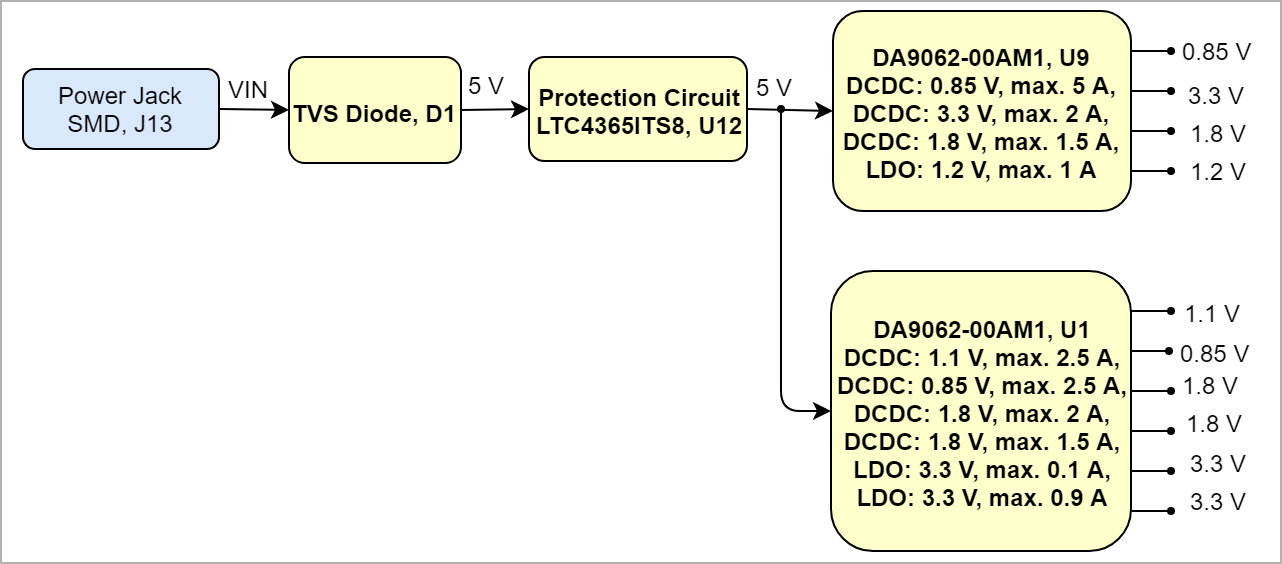 Image Modified Image Modified
|
|
Power-On Sequence
...
| anchor | Figure_PWR_PS |
|---|
| title | Power Sequency |
|---|
| Scroll Ignore |
|---|
Create DrawIO object here: Attention if you copy from other page, objects are only linked. |
| Scroll Only |
|---|
image link to the generate DrawIO PNG file of this page. This is a workaround until scroll pdf export bug is fixed |
PMICs will be reset after pressing Push Button BTN6 (POR_B).
Power Rails
| Scroll Title |
|---|
| anchor | Table_PWR_PR |
|---|
| title | Module power rails.Power Rails |
|---|
|
| Scroll Table Layout |
|---|
| orientation | portrait |
|---|
| sortDirection | ASC |
|---|
| repeatTableHeaders | default | style |
|---|
| widths | sortByColumn | 1 |
|---|
| sortEnabled | false |
|---|
| cellHighlighting | true |
|---|
|
| Power Rail Name | B2B Connector JM1 Pin | B2B Connector JM2 Pin | B2B Connector JM3 Pin | Direction | Notes | Direction | Notes |
|---|
| VIN | IN | Supply Voltage | | +5V | Out | J1...2 | | +3.3V | Out | J14, J10 |
|
Bank Voltages
| Scroll Title |
|---|
| anchor | Table_PWR_BV |
|---|
| title | Zynq SoC bank voltages.Bank Voltages |
|---|
|
| Scroll Table Layout |
|---|
| orientation | portrait |
|---|
| sortDirection | ASC |
|---|
| repeatTableHeaders | default | style | widths |
|---|
| sortByColumn | 1 |
|---|
| sortEnabled | false |
|---|
| cellHighlighting | true |
|---|
|
| Schematic Name | | Notes |
|---|
| Bank | 50326 | +3.3V | 3.3 V |
| | Bank | 2665 | + | 31. | 3V8V_PL | 31. | 3 8 V |
| | Bank | 6566 | +1.8V_PL | 1.8 V |
| | Bank 500 | +3.3V | 3.3 V |
| | Bank 501 | +3.3V | 3.3 V |
| | Bank 502 | +1.8V_ | PS1.8 PS | 1.8 V |
| | Bank 503 | +3.3V | 3.3 V |
| | Bank 504 | +1.1V_LPDDR4 | 1.1 V |
| | Bank 505 | +0.85V_MGTRAVCC | +1.8V_MGTRAVTT | 0.85 | V1.8 V | ??? |
|
|
Technical Specifications
Absolute Maximum Ratings
| Scroll Title |
|---|
| anchor | Table_TS_AMR |
|---|
| title | PS absolute maximum ratingsAbsolute Maximum Ratings |
|---|
|
| Scroll Table Layout |
|---|
| orientation | portrait |
|---|
| sortDirection | ASC |
|---|
| repeatTableHeaders | default | style |
|---|
| widths | sortByColumn | 1 |
|---|
| sortEnabled | false |
|---|
| cellHighlighting | true |
|---|
|
| Symbols | Description | Min | Max | Unit |
|---|
| VIN | Input Supply Voltage (J13) |
4 | 5| -3.5 | 7 | V | | T_STG | Storage Temperature | -40 | 85 | °C |
|
Recommended Operating Conditions
...
| Scroll Title |
|---|
| anchor | Table_TS_ROC |
|---|
| title | Recommended operating conditions.Operating Conditions |
|---|
|
| Scroll Table Layout |
|---|
| orientation | portrait |
|---|
| sortDirection | ASC |
|---|
| repeatTableHeaders | default | style |
|---|
| widths | sortByColumn | 1 |
|---|
| sortEnabled | false |
|---|
| cellHighlighting | true |
|---|
|
| Parameter | Min | Max | Units | Reference Document | VIN | 4 | 5.5 | V | | Units | Reference Document |
|---|
| VIN | 4 | 5.5 | V | Schematic "POWER" (Component: LTC4365ITS8) | | T_STG | 0 | 85 | °C | Zynq Ultrascale+ Data sheet |
|
Physical Dimensions
Module size: 100 mm × 100 mm. Please download the assembly diagram for exact numbers.
PCB thickness: 1,.48 mm
| Page properties |
|---|
|
In 'Physical Dimension' section, top and bottom view of module must be inserted, information regarding physical dimensions can be obtained through webpage for product in Shop.Trenz, (Download> Documents> Assembly part) for every SoM. For Example: for Module TE0728, Physical Dimension information can be captured by snipping tools from the link below: https://www.trenz-electronic.de/fileadmin/docs/Trenz_Electronic/Modules_and_Module_Carriers/5.2x7.6/TE0745/REV02/Documents/AD-TE0745-02-30-1I.PDF
|
...
| Scroll Title |
|---|
| anchor | Figure_TS_PD |
|---|
| title | Physical Dimension in mm |
|---|
|
| Scroll Ignore |
|---|
| draw.io Diagram |
|---|
| border | false |
|---|
| viewerToolbar | true |
|---|
| |
|---|
| fitWindow | false |
|---|
| diagramDisplayName | |
|---|
| lbox | true |
|---|
| revision | 1 |
|---|
| diagramName | TE0802_TS_PD |
|---|
| simpleViewer | false |
|---|
| width | 639 |
|---|
| links | auto |
|---|
| tbstyle | hidden |
|---|
| diagramWidth | 1228 |
|---|
|
Create DrawIO object here: Attention if you copy from other page, objects are only linked. |
| Scroll Only |
|---|
| scroll-pdf | true |
|---|
| scroll-office | true |
|---|
| scroll-chm | true |
|---|
| scroll-docbook | true |
|---|
| scroll-eclipsehelp | true |
|---|
| scroll-epub | true |
|---|
| scroll-html | true |
|---|
| image link to the generate DrawIO PNG file of this page. This is a workaround until scroll pdf export bug is fixed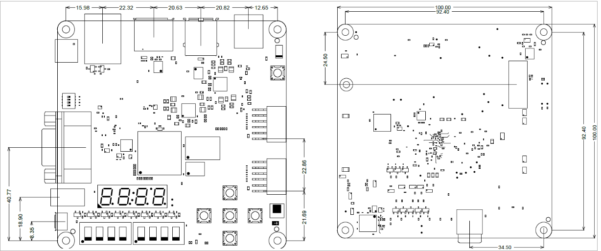 Image Added Image Added |
|
Currently Offered Variants
...
| Scroll Title |
|---|
| anchor | Table_VCP_SO |
|---|
| title | Trenz Electronic Shop Overview |
|---|
|
| Scroll Table Layout |
|---|
| orientation | portrait |
|---|
| sortDirection | ASC |
|---|
| repeatTableHeaders | default | style |
|---|
| widths | sortByColumn | 1 |
|---|
| sortEnabled | false |
|---|
| cellHighlighting | true |
|---|
|
|
Revision History
Hardware Revision History
...
| Scroll Title |
|---|
| anchor | Table_RH_HRH |
|---|
| title | Hardware Revision History |
|---|
|
| Scroll Table Layout |
|---|
| orientation | portrait |
|---|
| sortDirection | ASC |
|---|
| repeatTableHeaders | default | style | widths |
|---|
| sortByColumn | 1 |
|---|
| sortEnabled | false |
|---|
| cellHighlighting | true |
|---|
|
|
| Date | Revision | Changes | Documentation Link |
|---|
- | | | sortByColumn | 1 |
|---|
| sortEnabled | false |
|---|
| cellHighlighting | true |
|---|
|
| Date | Revision | Changes | Documentation Link |
|---|
| 2019-04-29 | 02 | - Added suppressor 1SMA5.0AT3G on power input
- Changed OV and UV protection range
- Changed VGA schematic
- USB page: VBUS resistor changed on 1K
| REV02 |
| 2018-10-17 | 01 | Release | REV01 |
Hardware revision number can be found on the PCB board together with the module model number separated by the dash.
| Scroll Title |
|---|
| anchor | Figure_RV_HRN |
|---|
| title | Board hardware revision number. |
|---|
| _RV_HRN | | title | Board Hardware Revision Number |
|---|
|
| Scroll Ignore |
|---|
| draw.io Diagram |
|---|
| border | false |
|---|
| viewerToolbar | true |
|---|
| |
|---|
| fitWindow | false |
|---|
| diagramDisplayName | |
|---|
| lbox | true |
|---|
| revision | 4 |
|---|
| diagramName | TE0802_RV_HRN |
|---|
| simpleViewer | true |
|---|
| width | |
|---|
| links | auto |
|---|
| tbstyle | hidden |
|---|
| diagramWidth | 128 |
|---|
|
|
| Scroll Only |
|---|
 Image Added Image Added
|
| Scroll Ignore |
|---|
Create DrawIO object here: Attention if you copy from other page, objects are only linked. |
| Scroll Only |
|---|
image link to the generate DrawIO PNG file of this page. This is a workaround until scroll pdf export bug is fixed |
|
Document Change History
| Page properties |
|---|
|
- Note this list must be only updated, if the document is online on public doc!
- It's semi automatically, so do following
Add new row below first Copy "Page Information Macro(date)" Macro-Preview, Metadata Version number, Author Name and description to the empty row. Important Revision number must be the same as the Wiki document revision number Update Metadata = "Page Information Macro (current-version)" Preview+1 and add Author and change description. --> this point is will be deleted on newer pdf export template - Metadata is only used of compatibility of older exports
|
...
| Scroll Title |
|---|
| anchor | Table_RH_DCH |
|---|
| title | Document change history.Change History |
|---|
|
| Scroll Table Layout |
|---|
| orientation | portrait |
|---|
| sortDirection | ASC |
|---|
| repeatTableHeaders | default | style |
|---|
| widths | sortByColumn | 1 |
|---|
| sortEnabled | false |
|---|
| cellHighlighting | true |
|---|
|
| Date | Revision | Contributor | Description |
|---|
| Page info |
|---|
| infoType | Modified date |
|---|
| dateFormat | yyyy-MM-dd |
|---|
| type | Flat |
|---|
|
| | Page info |
|---|
| infoType | Current version |
|---|
| prefix | v. |
|---|
| type | Flat |
|---|
| showVersions | false |
|---|
|
| | Page info |
|---|
| infoType | Modified by |
|---|
| type | Flat |
|---|
| showVersions | false |
|---|
|
Initial Release | | | 2020-11-19 | v.65 | Pedram Babakhani | | -- | all | | Page info |
|---|
| infoType | Modified users |
|---|
| type | Flat |
|---|
| showVersions | false |
|---|
|
| |
|
...