...
| Page properties |
|---|
|
Important General Note:
|
...
| Page properties |
|---|
|
Note for Download Link of the Scroll ignore macro: |
| Scroll pdf ignore |
|---|
Table of Contents |
...
The Trenz Electronic TE0802 is an evalution modulea development board integrating a Xilinx Zynq UltraScale+ . Other assembly options for the FPGA and the memory chips are available. Please contact us for further information.
Refer to http://trenz.org/te0802-info for the current online version of this manual and other available documentation.
...
| Page properties |
|---|
|
Note:
'Key Features' description: Important components and connector or other Features of the module
→ please sort and indicate assembly options |
- MPSoC: Xilinx Zynq XCZU2CG -1SBVA484E
- SDRAM: LPDDR4-3733 8Gb 256Mx32
- Xilinx Zynq UltraScale+ MPSoC
- RAM/Storages:
- SDRAM: LPDDR4 8Gb 256Mx16x 2
- SPI Flash
Storages:- SPI Flash 256Mb (32M x 8) 133 MHz
- EEPROMs 2Kb (256 x 8)
- EEPROMs 4Kb (512 x 8)
- Interfaces:
- USB JTAG/UART microUSB
- 1GB Ethernet RJ45
- USB 3.0 Host (Type A Connector)
- microSD Card
- M.2 SSD PCIe
- 3.5 mm Earphone Jack (PWM Output)
- Display
Interfaces: - Port
- DisplayPort
- VGA
- 4 Digit 7-Segment LED Display
- 8 LEDs
- Audio:
- Input:
- 5 User Buttons
- 8 Bit Slide Switches
- Reset Button
User I/O:Communication:
- 1GB Ethernet RJ45
- USB 3.0 Host (Type A Connector)
Debug - Power
- Dimension: 100mm x 100mm
Block Diagram
| Page properties |
|---|
|
add drawIO object here.
|
...
| Scroll Title |
|---|
| anchor | Figure_OV_BD |
|---|
| title | TE0802 Block Diagram |
|---|
|
| Scroll Ignore |
|---|
| draw.io Diagram |
|---|
| border | truefalse |
|---|
| viewerToolbar | true |
|---|
| |
|---|
| fitWindow | false |
|---|
| diagramDisplayName | |
|---|
| lbox | true |
|---|
| revision | 4 |
|---|
| diagramName | TE08202-02TE0802_OV_BD |
|---|
| simpleViewer | false |
|---|
| width | |
|---|
| links | auto |
|---|
| diagramWidthtbstyle | 611hidden |
|---|
| revisiondiagramWidth | 14638 |
|---|
|
|
| Scroll Only |
|---|
 Image Removed Image Removed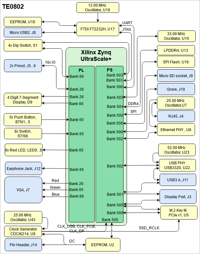 Image Added Image Added
|
|
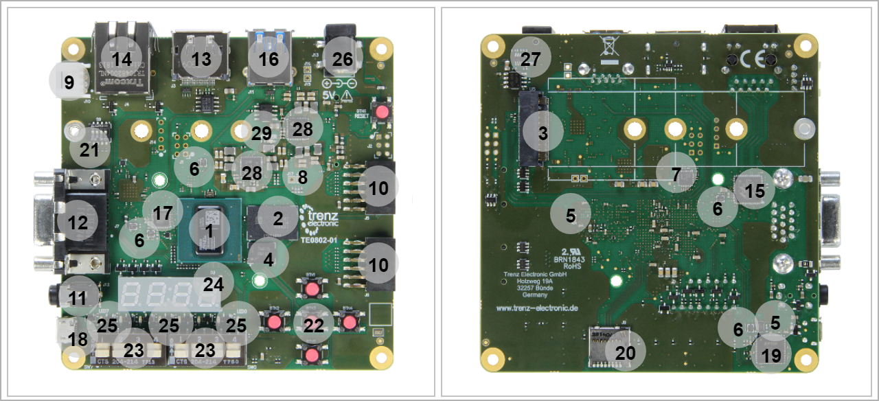
Main Components
| Page properties |
|---|
|
Notes : - Picture of the PCB (top and bottom side) with labels of important components
- Add List below
|
...
| Scroll Title |
|---|
| anchor | Figure_OV_MC |
|---|
| title | TE0802 Main Components (Picture shows Revision 01) |
|---|
|
| Scroll Ignore |
|---|
| draw.io Diagram |
|---|
| border | truefalse |
|---|
| viewerToolbar | true |
|---|
| |
|---|
| fitWindow | false |
|---|
| diagramDisplayName | |
|---|
| lbox | true |
|---|
| revision | 10 |
|---|
| diagramName | TE0802_ | diagramName | TE0802_OV_MC |
|---|
| simpleViewer | falsetrue |
|---|
| width |
|---|
| diagramWidth | 602 |
|---|
| | links | auto |
|---|
| tbstyle | hidden |
|---|
| diagramWidth | 640 | revision | 8 |
|---|
|
|
| Scroll Only |
|---|
|
|
- Xilinx Zynq UltraScale+ MPSoc, U14
- LPDDR4 SDRAM, U13
- M.2 Key M PCIe x1, U5
- SPI Flash Memory, U16
- EEPROM, U2, U18
- Oscillator, U15, U7, U19, U23, U43
- Clock Generator, U8
- Clock Generator Programming Connector, J14
- Grove Connector, J10
- Pmod Host Socket, J5...6
- Headphone Jack, J12
- D-Sub Connector, J7
- DisplayPort, J3
- RJ45 Socket, J4
- Ethernet PHY, U6
- USB Type A, J11
- USB 2.0 PHY, U22
- Micro USB 2.0 Type B, J8
- FTDI USB 2.0 to JTAG/UART Converter, U17
- microSD Card, J9
- Slide Switch, S1
- Push Button, BTN1...5
- DIP Switch, S7...8
- 4 Digit 7-Segment LED Display, D9
- 8x LEDs (Red), LED0...7
- Power Jack, J13
- Overvoltage/Undervoltage/Reverse Supply Protector, U12
- Power Management Integrated Circuit (PMIC), U1, U9
- Power Good LED (Green), D12
...
| Scroll Title |
|---|
| anchor | Table_OV_IDS |
|---|
| title | Initial Delivery State of Programmable Devices on the Module |
|---|
|
| Scroll Table Layout |
|---|
| orientation | portrait |
|---|
| sortDirection | ASC |
|---|
| repeatTableHeaders | default | style | widths |
|---|
| sortByColumn | 1 |
|---|
| sortEnabled | false |
|---|
| cellHighlighting | true |
|---|
|
Storage device name | Content | Notes |
|---|
SPI Flash (U16) | Not programmed |
| | EEPROM (U2) | Not programmed | Except Ethernet MAC | | EEPROM (U18) | Programmed | FTDI Configuration | | LPDDR4 SDRAM (U13) | Not programmed |
|
|
Configuration Signals
| Page properties |
|---|
|
- Overview of Boot Mode, Reset, Enables.
|
Bootmode signals must be set through DIP Switch S1.
| Scroll Title |
|---|
| anchor | Table_OV_BP |
|---|
| title | Boot process.Process |
|---|
|
| Scroll Table Layout |
|---|
| orientation | portrait |
|---|
| sortDirection | ASC |
|---|
| repeatTableHeaders | default | style | widths |
|---|
| sortByColumn | 1 |
|---|
| sortEnabled | false |
|---|
| cellHighlighting | true |
|---|
|
MODE Signal State | MODE1 S1-2(B) | MODE0 |
|---|
MODE1100101 | QSPI(24b)110111
|
Reset setting is available through Push Button BTN6.
| Scroll Title |
|---|
| anchor | Table_OV_RST |
|---|
| title | Reset process.Process |
|---|
|
| Scroll Table Layout |
|---|
| orientation | portrait |
|---|
| sortDirection | ASC |
|---|
| repeatTableHeaders | default | style | widths |
|---|
| sortByColumn | 1 |
|---|
| sortEnabled | false |
|---|
| cellHighlighting | true |
|---|
|
Signal | Connected to | Note |
|---|
POR_B | BTN6, Push Button | Connected to nRESET |
|
Signals, Interfaces and Pins
...
| Scroll Title |
|---|
| anchor | Table_SIP_B2B |
|---|
| title | General I/O to Pin Header and Connectors Information |
|---|
|
| Scroll Table Layout |
|---|
| orientation | portrait |
|---|
| sortDirection | ASC |
|---|
| repeatTableHeaders | default | style | widths |
|---|
| sortByColumn | 1 |
|---|
| sortEnabled | false |
|---|
| cellHighlighting | true |
|---|
|
| FPGA Bank | Connector | I/O Signal Count | Voltage Level | Notes |
|---|
| Bank 503 |
J8, ()J9Micro SD Card)J4, (RJ45) | Bank 505 | J11, (USB 3.0) | 2 Differential Pairs | 0.85 V | U5, (SSD M.2) | Bank 505 | J3, (Display Port Connector) | | over FTDI) | 4 Single Ended | 3.3 V | JTAG | | Bank 500 | Micro USB, J8 (over FTDI) | 2 Single Ended | 3.3 V | UART | | Bank 500 | Micro SD Card, J9 | 7 |
2 Differential Pairs | 0.85 V | Bank 26 | J7, (D-Sub Host Socket) | 2 65, 66,J7, (D-Sub Host Socket) | | 502 | ETH RJ45, J4 (over ETH PHY) | 14 |
12 65J12 Headphone Single Ended1.8 V | Bank 500 | J10, (Grove Connector| .0, J11 (USB2 over USB PHY) | 2 Differential Pairs, 12 Single Ended |
3.3 V | Bank 26 | J5 (Pmod Host Socket) | 8 Single Ended | | -- / 1.8V |
| Bank 505, 501 | SSD M.2, U5 | 2 Differential Pairs, 5 Single Ended | -- / 3.3 V |
| | Bank 505, 501 | Display Port Connector, J3 | 2 Differential Pairs, 5 Single Ended | --/ 3.3 V |
| | Bank 26 |
J6 (Pmod | , 65, 66, | D-Sub Host Socket (VGA), J7 |
8 V |
Micro USB 2.0 Connector
FTDI FT2232 (U17) can be accessed through micro USB 2.0 B connector (J8) for JTAG (channel A). Channel B is connected to the FPGA and can be used for UART.
Micro SD Card Connector
| V / 1.8 V / 1.8 V |
| | Bank 65 | Earphone, J12 | 3 Single Ended | 1.8 V |
| | Bank 500 | Grove Connector, J10 | 2 Single Ended | 3.3 V |
| | Bank 26 | Pmod Host Socket, J5 | 8 Single Ended | 3.3 V |
| | Bank 26 | Pmod Host Socket, J6 | 8 Single Ended | 3.3 V |
|
|
Micro SD Card
TE0802 TEI0802 is equipped with a micro SD card connector (J9).
| Scroll Title |
|---|
| anchor | Table_SIP_VGASD |
|---|
| title | Display Port Socket Micro SD Card Connector Information |
|---|
|
| Scroll Table Layout |
|---|
| orientation | portrait |
|---|
| sortDirection | ASC |
|---|
| repeatTableHeaders | default | style |
|---|
| widths | sortByColumn | 1 |
|---|
| sortEnabled | false |
|---|
| cellHighlighting | true |
|---|
|
| Schematic | Corresponding Signals | Connected to | Notes |
|---|
|
RJ45 Connector
TEI0802 is equipped with a RJ45 connector and an Ethernet PHYs. RJ45 connectors J4 is connected to Ethernet PHYs U6.
...
| anchor | Table_SIP_RJ45 |
|---|
| title | RJ45 Connector Information |
|---|
| SD_DAT0 | MIO 13, FPGA Bank 500 |
| | SD_DAT1 | MIO 14, FPGA Bank 500 |
| | SD_DAT2 | MIO 15, FPGA Bank 500 |
| | SD_DAT3 | MIO 16, FPGA Bank 500 |
| | SD_CLK | MIO 22, FPGA Bank 500 |
| | SD_CMD | MIO 21, FPGA Bank 500 |
| | SD_CD | MIO 24, FPGA Bank 500 |
|
|
RJ45 Connector
TE0802 is equipped with a RJ45 connector and an Ethernet PHYs. RJ45 connector J4 is connected to Ethernet PHYs U6
...
USB Connector
TEI0802 is equipped with a USB connector (J11).
| Scroll Title |
|---|
| anchor | Table_SIP_VGARJ45 |
|---|
| title | USB Socket RJ45 Connector Information |
|---|
|
| Scroll Table Layout |
|---|
| orientation | portrait |
|---|
| sortDirection | ASC |
|---|
| repeatTableHeaders | default | style |
|---|
| widths | sortByColumn | 1 |
|---|
| sortEnabled | false |
|---|
| cellHighlighting | true |
|---|
|
| Corresponding Signals | Connected to |
...
...
TEI0802 is equipped with a SSD M.2 connector (U5).
...
| anchor | Table_SIP_VGA |
|---|
| title | SSD M.2 Connector Information |
|---|
| PHY_MDI0_P | MDIP[0] |
| | 3 | PHY_MDI0_N | MDIN[0] |
| | 4 | PHY_MDI1_P | MDIP[1] |
| | 5 | PHY_MDI1_N | MDIN[1] |
| | 6 | PHY_MDI2_P | MDIP[2] |
| | 7 | PHY_MDI2_N | MDIN[2] |
| | 8 | PHY_MDI3_P | MDIP[3] |
| | 9 | PHY_MDI3_N | MDIN[3] |
|
|
USBs Sockets
TE0802 is equipped with a Micro USB2.0 B connector J8 and a USB3.0 connector J11.
FTDI FT2232 (U17) can be accessed through Micro USB 2.0 B connector (J8) for JTAG (channel A). Channel B is connected to the FPGA and can be used for UART.
...
Display Port Connector
TEI0802 is equipped with a Display Port connector (J3).
| scroll-title |
|---|
| anchor | Table_SIP_VGAUSB2 |
|---|
| title | Display Port USB2.0 B Socket Information |
|---|
|
| Scroll Table Layout |
|---|
| orientation | portrait |
|---|
| sortDirection | ASC |
|---|
| repeatTableHeaders | default | style |
|---|
| widths | sortByColumn | 1 |
|---|
| sortEnabled | false |
|---|
| cellHighlighting | true |
|---|
|
| Corresponding Signals | DP_TX_L0_P/N | DP0_TX_P/N | Bank 505 | DP_TX_L1_P/N | DP1_TX_P/N | Bank 505 | DP_TX_AUX_P/N | DP_AUX_TX/RX | Bank 501 | |
D-Sub Connector
TEI0802 is equipped with a D-Sub connector (J7).
|
|---|
| D- | D_N | FTDI, U17 |
| | D+ | D_P | FTDI, U17 |
| | Vbus | USB_VBUS | GND |
|
|
| Scroll Title |
|---|
| anchor | Table_SIP_VGAUSB3 |
|---|
| title | D-Sub Connector USB3.0 A Socket Information |
|---|
|
| Scroll Table Layout |
|---|
| orientation | portrait |
|---|
| sortDirection | ASC |
|---|
| repeatTableHeaders | default | style | widths |
|---|
| sortByColumn | 1 |
|---|
| sortEnabled | false |
|---|
| cellHighlighting | true |
|---|
|
| Schematic | Corresponding Signals| VGA_RED | VGA_R0...3 | Bank 65 | Red Channel | | VGA_GREEN | VGA_G0...3 | Bank 65 | Green Channel | | VGA_BLUE | VGA_B0...3 | Bank 66 | Blue Channel | | VGA_RGB_HSYNC | VGA_HS | Bank 26 | Horizontal Sync | | VGA_RGB_VSYNC | VGA_VS | Bank 26 | Vertical Sync | |
Headphone Connector
| D- | USB0_D_N | USB PHY, U22 |
| | D+ | USB0_D_P | USB PHY, U22 |
| | StdA_SSRX- | USB_RX2_N | FPGA Bank 505 |
| | StdA_SSRX+ | USB_RX2_P | FPGA Bank 505 |
| | StdA_SSTX- | USB_TX2_N | FPGA Bank 505 |
| | StdA_SSTX+ | USB_TX2_P | FPGA Bank 505 |
| | VBUS | VBUS | USB PHY, U22 |
|
|
SSD M.2 Connector
TE0802 is equipped with a SSD M.2 connector (U5TEI0802 is equipped with a headphone connector (J12).
| Scroll Title |
|---|
| anchor | Table_SIP_VGASSD |
|---|
| title | Headphone SSD M.2 Connector Information |
|---|
|
| Scroll Table Layout |
|---|
| orientation | portrait |
|---|
| sortDirection | ASC |
|---|
| repeatTableHeaders | default | style | widths |
|---|
| sortByColumn | 1 |
|---|
| sortEnabled | false |
|---|
| cellHighlighting | true |
|---|
|
|
Grove Connector
TEI0802 is equipped with a grove connector (J10).
...
| anchor | Table_SIP_VGA |
|---|
| title | Grove Connector Information |
|---|
| PERn0/SATA-B+ | SSD_RX3_N | Pin M22, FPGA Bank 505 |
| | PERp0/SATA-B- | SSD_RX3_P | Pin M21, FPGA Bank 505 |
| | PERn0/SATA-A+ | SSD_TXC3_N | Pin K22, FPGA Bank 505 |
| | PERp0/SATA-A- | SSD_TXC3_P | Pin M21, FPGA Bank 505 |
| | REFCLKN | SSD_RCLK_N | Pin 9, Clock Generator U8 |
| | REFCLKP | SSD_RCLK_P | Pin 10, Clock Generator U8 |
| | DAS/DSS# | SSD_DAS | MIO35, FPGA Bank 501 |
| | DEVSLP | SSD_SLEEP | MIO32, FPGA Bank 501 |
| | PERST# | SSD_PERSTn | MIO31, FPGA Bank 501 |
| | CLKREQ# | SSD_CLKRQ | MIO33, FPGA Bank 501 |
| | PEWake# | SSD_WAKE | MIO34, FPGA Bank 501 |
|
|
Display Port Connector
TE0802 is equipped with a Display Port connector (J3)
...
Pmod Host Socket
TEI0802 has 2 Pmod 2x6 host sockets which are connected to the FPGA.
| Scroll Title |
|---|
| anchor | Table_SIP_SMDDP |
|---|
| title | Pmod SMD Host Display Port Socket Information |
|---|
|
| Scroll Table Layout |
|---|
| orientation | portrait |
|---|
| sortDirection | ASC |
|---|
| repeatTableHeaders | default | style |
|---|
| widths | sortByColumn | 1 |
|---|
| sortEnabled | false |
|---|
| cellHighlighting | true |
|---|
|
Designator| Schematic | Corresponding Signals | Connected |
|---|
to J5 | PMOD_A0...7 | Bank 26 | J6 | PMOD_B0...7 | Bank 26 | |
On-board Peripherals
| Page properties |
|---|
|
Notes : - add subsection for every component which is important for design, for example:
- Two 100 Mbit Ethernet Transciever PHY
- USB PHY
- Programmable Clock Generator
- Oscillators
- eMMCs
- RTC
- FTDI
- ...
- DIP-Switches
- Buttons
- LEDs
|
| Page properties |
|---|
|
Notes : In the on-board peripheral table "chip/Interface" must be linked to the corresponding chapter or subsection |
...
| anchor | Table_OBP |
|---|
| title | On board peripherals |
|---|
...
| DP_TX_L0_P/N | DP0_TX_P/N | Pin A19/A20, FPGA Bank 505 |
| | DP_TX_L1_P/N | DP1_TX_P/N | Pin C19/C20, FPGA Bank 505 |
| | DP_TX_AUX_P/N | DP_AUX_TX/RX | MIO27, MIO30, FPGA Bank 501 |
|
|
D-Sub Connector
TE0802 is equipped with a D-Sub connector (J7).
| Scroll Title |
|---|
| anchor | Table_SIP_VGA |
|---|
| title | D-Sub Connector Information |
|---|
|
| Scroll Table Layout |
|---|
| orientation | portrait |
|---|
| sortDirection | ASC |
|---|
| repeatTableHeaders | default |
|---|
| sortByColumn | 1 |
|---|
| sortEnabled | false |
|---|
| cellHighlighting | true |
|---|
|
| Schematic | Corresponding Signals | Connected to | Notes |
|---|
| VGA_RED | VGA_R0...3 | Bank 65 | Red Channel | | VGA_GREEN | VGA_G0...3 | Bank 65 | Green Channel | | VGA_BLUE | VGA_B0...3 | Bank 66 | Blue Channel | | VGA_RGB_HSYNC | VGA_HS | Bank 26 | Horizontal Sync | | VGA_RGB_VSYNC | VGA_VS | Bank 26 | Vertical Sync |
|
Headphone Connector
TE0802 is equipped with a headphone connector (J12).
| Scroll Title |
|---|
| anchor | Table_SIP_HP |
|---|
| title | Headphone Connector Information |
|---|
|
| Scroll Table Layout |
|---|
| orientation | portrait |
|---|
| sortDirection | ASC |
|---|
| repeatTableHeaders | default |
|---|
| sortByColumn | 1 |
|---|
| sortEnabled | false |
|---|
| cellHighlighting | true |
|---|
|
| Schematic | Connected to | Notes |
|---|
| JACKSNS | Pin F3, FPGA Bank 65 |
| | PWM_R | Pin F4, FPGA Bank 65 |
| | PWM_L | Pin E3, FPGA Bank 65 |
|
|
Grove Connector
TE0802 is equipped with a grove connector (J10).
| Scroll Title |
|---|
| anchor | Table_SIP_Grove |
|---|
| title | Grove Connector Information |
|---|
|
...
Quad SPI Flash Memory
| Page properties |
|---|
|
Notes : Minimum and Maximum density of quad SPI flash must be mentioned for other assembly options. |
| Scroll Title |
|---|
| anchor | Table_OBP_SPI |
|---|
| title | Quad SPI Interface MIOs and Pins |
|---|
|
| Scroll Table Layout |
|---|
| orientation | portrait |
|---|
| sortDirection | ASC |
|---|
| repeatTableHeaders | default | style |
|---|
| widths | sortByColumn | 1 |
|---|
| sortEnabled | false |
|---|
| cellHighlighting | true |
|---|
|
MIO PinU16 Pin| MIO0 | MIO0 | B2 | SPI_CLK | | MIO1 | MIO1 | D2 | SPI_DQ1 | | MIO2 | MIO2 | C4 | SPI_DQ2 | | MIO3 | MIO3 | D4 | SPI_DQ3 | | MIO4 | MIO4 | D3 | SPI_DQ0 | | MIO5 | MIO5 | C2 | SPI_CS | |
LPDDR4 SDRAM
| Page properties |
|---|
|
Notes : Minimum and Maximum density of DDR3 SDRAM must be mentioned for other assembly options. (pay attention to supported address length for DDR3) |
The TE0802 evaluation board has 1 GByte volatile LPDDR4 SDRAM IC for storing user application code and data. The details depends on the assembly option.
- Part number:
- Supply voltage:
- Speed:
- NOR Flash
- Temperature:
EEPROM
| Grove_SCL0 | MIO18, FPGA Bank 500 |
| | Grove_SDA0 | MIO19, FPGA Bank 500 |
|
|
Pmod Sockets
TE0802 has 2 Pmod 2x6 host sockets which are connected to the FPGA.
| Scroll Title |
|---|
| anchor | Table_SIP_PMOD |
|---|
| title | Pmod SMD Host Socket Information |
|---|
|
| Scroll Table Layout |
|---|
| orientation | portrait |
|---|
| sortDirection | ASC |
|---|
| repeatTableHeaders | default |
|---|
| sortByColumn | 1 |
|---|
| sortEnabled | false |
|---|
| cellHighlighting | true |
|---|
|
| Designator | Signals | Connected to | Notes |
|---|
| J5 | PMOD_A0...7 | Bank 26 |
| | J6 | PMOD_B0...7 | Bank 26 |
|
|
Test Points
| Scroll Title |
|---|
| anchor | Table_OBPSIP_EEPTestPoint |
|---|
| title | I2C EEPROM interface MIOs and pinsTest Points Information |
|---|
|
| Scroll Table Layout |
|---|
| orientation | portrait |
|---|
| sortDirection | ASC |
|---|
| repeatTableHeaders | default |
|---|
| style | |
|---|
| widths | |
|---|
| sortByColumn | 1 |
|---|
| sortEnabled | false |
|---|
| cellHighlighting | true |
|---|
|
|
| Scroll Title |
|---|
| anchor | Table_OBP_I2C_EEPROM |
|---|
| title | I2C Address for EEPROM |
|---|
|
| Scroll Table Layout |
|---|
| orientation | portrait |
|---|
| sortDirection | ASC |
|---|
| repeatTableHeaders | default |
|---|
style | widths | | sortByColumn | 1 |
|---|
| sortEnabled | false |
|---|
| cellHighlighting | true |
|---|
| MIO Pin | I2C Address | Designator | Notes |
|---|
MIO8...9 | 0x50 | U2 |
USB PHY
The TEI0802 is equipped with a USB PHY.
...
| anchor | Table_OBP_USB |
|---|
| title | USB PHY Connections and Pins |
|---|
...
Ethernet PHY
The TEI0802 is equipped with an Ethernet PHY (U6) which is connected to RJ45 (J) connector.
...
| anchor | Table_OBP_ETH |
|---|
| title | Ethernet PHY Connections and Pins |
|---|
...
| TP1 | +1.1V_LPDDR4 |
| | TP2 | +1.8V_MGTRAVTT |
| | TP3 | +1.8V_PL |
| | TP4 | FT_B_TX |
| | TP5 | DP_TX_PWR |
| | TP6 | GND |
| | TP7 | GND |
| | TP8 | PMIC2_SDA |
| | TP9 | PMIC2_TP |
| | TP10 | ONKEY2 |
| | TP11 | PMIC2_SCL |
| | TP12 | DP_TX_HPD |
| | TP13 | DP_TX_PWR |
| | TP14 | INT_SCL1 |
| | TP15 | INT_SDA1 |
| | TP16 | FT_B_RX |
| | TP17 | CLOCKDIST_OE |
| | TP18 | +0.85V_VCCINT |
| | TP19 | +3.3V |
| | TP20 | +1.8V_PS |
| | TP21 | ERR_STATUS |
| | TP22 | +1.2V_PSPLL |
| | TP23 | GND |
| | TP24 | GND |
| | TP25 | PMIC1_SCA |
| | TP26 | PMIC1_SDA |
| | TP27 | ONKEY1 |
| | TP28 | PMIC1_TP |
| | TP29 | POR_B |
| | TP30 | PSBATT |
| | TP31 | SRST_B |
| | TP32 | DONE |
| | TP33 | INIT_B |
| | TP34 | VBUS |
| | TP35 | USB_VBUS |
| | TP36 | PROG_B |
| | TP37 | ERR_OUT |
|
|
On-board Peripherals
| Page properties |
|---|
|
Notes : - add subsection for every component which is important for design, for example:
- Two 100 Mbit Ethernet Transciever PHY
- USB PHY
- Programmable Clock Generator
- Oscillators
- eMMCs
- RTC
- FTDI
- ...
- DIP-Switches
- Buttons
- LEDs
|
| Page properties |
|---|
|
Notes : In the on-board peripheral table "chip/Interface" must be linked to the corresponding chapter or subsection |
| Scroll Title |
|---|
| anchor | Table_OBP |
|---|
| title | On-board Peripherals |
|---|
|
| Scroll Table Layout |
|---|
| orientation | portrait |
|---|
| sortDirection | ASC |
|---|
| repeatTableHeaders | default |
|---|
| sortByColumn | 1 |
|---|
| sortEnabled | false |
|---|
| cellHighlighting | true |
|---|
|
|
Quad SPI Flash Memory
| Page properties |
|---|
|
Notes : Minimum and Maximum density of quad SPI flash must be mentioned for other assembly options. |
he TE0802 evaluation board has one single QSPI flash connected as x4. Flash size depends on the assembly option, default 32MB
| Scroll Title |
|---|
| anchor | Table_OBP_SPI |
|---|
| title | Quad SPI Interface MIOs |
|---|
|
...
RJ45 - Green LED, J
...
RJ45 - Yellow LED, J
...
FTDI FT2232
The FTDI chip U17 converts signals from USB 2.0 to a variety of standard serial and parallel interfaces. Refer to the FTDI data sheet for more information about the capacity of the FT2232H chip.
Channel A of FTDI FT2232H chip is used in MPPSE mode for JTAG. Channel B is used in UART mode.
The configuration of FTDI FT2232H chip is pre-programmed on the EEPROM U18.
| Scroll Title |
|---|
| anchor | Table_OBP_FTDI |
|---|
| title | FTDI Chip Interfaces and Pins |
|---|
|
| Scroll Table Layout |
|---|
| orientation | portrait |
|---|
| sortDirection | ASC |
|---|
| repeatTableHeaders | default | style | widths |
|---|
| sortByColumn | 1 |
|---|
| sortEnabled | false |
|---|
| cellHighlighting | true |
|---|
|
FTDI Chip Signal NameConnected toADBUS0TCK| Bank | JTAG interface | | ADBUS1 | TDI | Bank | | ADBUS2 | TDO | Bank | | ADBUS3 | TMS | Bank | | BDBUS0 | FT_B_TX | Bank | UART | | BDBUS1 | FT_B_RX | Bank | UART | EECS | EECS | EEPROM, U18 | EECLK | EECLK | EEPROM, U18 | EEDATA | EEDATA | EEPROM, U18 | OSCI | - | 12 MHz Oscillator, U19 | DM | D_N | Micro USB 2.0, J8 | DP | D_P | Micro USB 2.0, J8 | |
Clock Generator
The TEI0802 is equipped with a clock generator (U8).
| B2 | SPI_CLK | | MIO1 | MIO1 | D2 | SPI_DQ1 | | MIO2 | MIO2 | C4 | SPI_DQ2 | | MIO3 | MIO3 | D4 | SPI_DQ3 | | MIO4 | MIO4 | D3 | SPI_DQ0 | | MIO5 | MIO5 | C2 | SPI_CS |
|
LPDDR4 SDRAM
| Page properties |
|---|
|
Notes : Minimum and Maximum density of DDR3 SDRAM must be mentioned for other assembly options. (pay attention to supported address length for DDR3) |
The TE0802 evaluation board has 1 GByte volatile LPDDR4 SDRAM IC (U13) for storing user application code and data. The details depends on the assembly option.
- Part number: IS43LQ32256A-062BLI
- Supply voltage: 1.06 -1.17 V
- Speed: 1600 MHz
- Temperature: -40 to +85 C
EEPROM
| Scroll Title |
|---|
| anchor | Table_OBP_FPGA_EEP |
|---|
| title | I2C FPGA EEPROM Interface MIOs |
|---|
|
| Scroll Title |
|---|
| anchor | Table_OBP_CLK_GEN |
|---|
| title | Clock Generator Connections and Pins |
|---|
|
| Scroll Table Layout |
|---|
| orientation | portrait |
|---|
| sortDirection | ASC |
|---|
| repeatTableHeaders | default | style | widths |
|---|
| sortByColumn | 1 |
|---|
| sortEnabled | false |
|---|
| cellHighlighting | true |
|---|
|
Clock Generator | Signal Schematic Names | Note | |
...
| Schematic | U2 Pin | Notes |
|---|
| MIO8 | Int_SCL1 | SCL |
| | MIO9 | Int_SDA1 | SDA |
|
|
| Scroll Title |
|---|
| anchor | Table_OBP_I2C_FPGA_CLKEEP |
|---|
| title | OscillatorsI2C Address for FPGA EEPROM |
|---|
|
| Scroll Table Layout |
|---|
| orientation | portrait |
|---|
| sortDirection | ASC |
|---|
| repeatTableHeaders | default | style |
|---|
| widths | sortByColumn | 1 |
|---|
| sortEnabled | false |
|---|
| cellHighlighting | true |
|---|
|
DesignatorDescriptionFrequency| Note | U43 | Clock for Clock Generator | 25 MHz | U15 | 33 MHz | U7 | 25 MHz | U23 | Clock for USB | 52 MHz | |
7-Segment Display
The TEI0802 has a 4-Digit-7-Segment LED display.
| Notes |
|---|
| 4AA025E48T-I/OT | 0x50 | U2 | EEPROM with MAC |
|
| Scroll Title |
|---|
| anchor | Table_OBP_FTDI_7SEGEEP |
|---|
| title | 7-Segment LED I2C FTDI EEPROM Interface Pins |
|---|
|
| Scroll Table Layout |
|---|
| orientation | portrait |
|---|
| sortDirection | ASC |
|---|
| repeatTableHeaders | default | style | widths |
|---|
| sortByColumn | 1 |
|---|
| sortEnabled | false |
|---|
| cellHighlighting | true |
|---|
|
Connected to | A/L1 | SEG_CA | B/L2 | SEG_CB | C/L3 | SEG_CC | D | SEG_CD | E | SEG_CE | F | SEG_CF | G | SEG_CG | DP | SEG_CDP | A1 | SEG_AN | A2 | SEG_AN4 | A3 | SEG_AN3 | A4 | SEG_AN2 | L1-L3 | SEG_AN1 | |
User LEDs
| CS | EECS | 1 | FTDI | | CLK | EECLK | 2 | FTDI | | DIN/DO | EEDATA | 3/4 | FTDI |
|
USB ULPI PHY
The TE802 is equipped with a USB ULPI PHY.
| Scroll Title |
|---|
| anchor | Table_OBP_USB |
|---|
| title | USB ULPI PHY Connections and Pins |
|---|
|
| Scroll Table Layout |
|---|
| orientation | portrait |
|---|
| sortDirection | ASC |
|---|
| repeatTableHeaders | default |
|---|
|
|
| Scroll Title |
|---|
| anchor | Table_OBP_LED |
|---|
| title | On-board LEDs |
|---|
|
| Scroll Table Layout |
|---|
| orientation | portrait |
|---|
| sortDirection | ASC |
|---|
| repeatTableHeaders | default |
|---|
| style | widths |
|---|
| sortByColumn | 1 |
|---|
| sortEnabled | false |
|---|
| cellHighlighting | true |
|---|
|
| USB PHY Pin | Signal Schematic Names |
|---|
Color | Active Level | LED0...7 | Red | Bank 65 | High | D12 | Green | U9, PMIC | High | |
Push Buttons
...
| anchor | Table_OBP_PBTN |
|---|
| title | On-board Push Buttons |
|---|
...
DATA0 | USB0_DATA0 | MIO56, FPGA Bank 502 |
| | DATA1 | USB0_DATA1 | MIO57, FPGA Bank 502 |
| | DATA2 | USB0_DATA2 | MIO54, FPGA Bank 502 |
| | DATA3 | USB0_DATA3 | MIO59, FPGA Bank 502 |
| | DATA4 | USB0_DATA4 | MIO60, FPGA Bank 502 |
| | DATA5 | USB0_DATA5 | MIO61, FPGA Bank 502 |
| | DATA6 | USB0_DATA6 | MIO62, FPGA Bank 502 |
| | DATA7 | USB0_DATA7 | MIO63, FPGA Bank 502 |
| | DIR | USB0_DIR | MIO53, FPGA Bank 502 |
| | NXT | USB0_NXP | MIO55, FPGA Bank 502 |
| | STP | USB0_STP | MIO58, FPGA Bank 502 |
| | RESETB | USB0_RST_N | MIO38, FPGA Bank 501 |
| | CPEN | USB0_VBUS_EN | Pin 1, U21 (Current-limited Power Switch) |
| | VBUS | VBUS | Pin 8, U21 (Current-limited Power Switch). Pin 1, J11 (USB Connector) |
| | ID | USB0_ID | Pulled-down to GND |
| | DP | USB0_D_P | Pin 3, J11 (USB Connector) |
| | DM | USB0_D_N | Pin 2, J11 (USB Connector) |
| | REFCLK | USB0_RCLK | Pin 3, U23 (Oscillator) |
| | CLKOUT | USB0_CLK | MIO52, FPGA Bank 502 |
|
|
Ethernet PHY
The TE0802 is equipped with an Ethernet PHY (U6) which is connected to RJ45 (J4) connector.
...
DIP Switch
...
| anchor | Table_OBP_DIP_SWITCH |
|---|
| title | DIP Switch |
|---|
...
Switch
| Scroll Title |
|---|
| anchor | Table_OBP_SWITCHETH |
|---|
| title | SwitchEthernet PHY Connections and Pins |
|---|
|
| Scroll Table Layout |
|---|
| orientation | portrait |
|---|
| sortDirection | ASC |
|---|
| repeatTableHeaders | default | style | widths |
|---|
| sortByColumn | 1 |
|---|
| sortEnabled | false |
|---|
| cellHighlighting | true |
|---|
|
| Ethernet PHY Pin | Signal Schematic Names |
|---|
ColorConnected toActive Level | Note | |
Power and Power-On Sequence
...
In 'Power and Power-on Sequence' section there are three important digrams which must be drawn:
- Power on-sequence
- Power distribution
- Voltage monitoring circuit
| Note |
|---|
For more information regarding how to draw diagram, Please refer to "Diagram Drawing Guidline" . |
Power Supply
Power supply with minimum current capability of 3 A for system startup is recommended.
Power Consumption
...
| anchor | Table_PWR_PC |
|---|
| title | Power Consumption |
|---|
...
* TBD - To Be Determined
Power Distribution Dependencies
...
| anchor | Figure_PWR_PD |
|---|
| title | Power Distribution |
|---|
...
| Scroll Only |
|---|
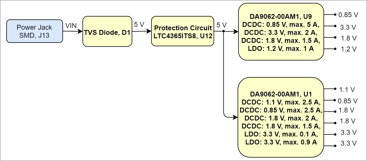 Image Removed Image Removed
|
Power-On Sequence
...
| anchor | Figure_PWR_PS |
|---|
| title | Power Sequency |
|---|
| Scroll Ignore |
|---|
Create DrawIO object here: Attention if you copy from other page, objects are only linked. |
| Scroll Only |
|---|
image link to the generate DrawIO PNG file of this page. This is a workaround until scroll pdf export bug is fixed |
| TXD0 | ETH_TXD0 | MIO65, FPGA Bank 502 |
| | TXD1 | ETH_TXD1 | MIO66, FPGA Bank 502 |
| | TXD2 | ETH_TXD2 | MIO67, FPGA Bank 502 |
| | TXD3 | ETH_TXD3 | MIO68, FPGA Bank 502 |
| | TX_CTRL | ETH_TXCTL | MIO69, FPGA Bank 502 |
| | TX_CLK | ETH_CLK | MIO64, FPGA Bank 502 |
| | MDIO | ETH_MDIO | MIO77, FPGA Bank 502 | Pulled-up to +1.8V_PS. | | MDC | ETH_MDC | MIO76, FPGA Bank 502 |
| | MDIP[0] | PHY_MDI0_P | Pin2, J4 (RJ45) |
| | MDIN[0] | PHY_MDI0_N | Pin3, J4 (RJ45) |
| | MDIP[1] | PHY_MDI1_P | Pin4, J4 (RJ45) |
| | MDIN[1] | PHY_MDI1_N | Pin5, J4 (RJ45) |
| | MDIP[2] | PHY_MDI2_P | Pin6, J4 (RJ45) |
| | MDIN[2] | PHY_MDI2_N | Pin7, J4 (RJ45) |
| | MDIP[3] | PHY_MDI3_P | Pin8, J4 (RJ45) |
| | MDIN[3] | PHY_MDI3_N | Pin9, J4 (RJ45) |
| | LED[0] | PHY_LED0 | LED, J4 (RJ45) |
| | LED[1] | PHY_LED1 | LED, J4 (RJ45) |
| | CONFIG | - | - | Pulled-up to +1.8V_PS. | | XTAL_IN | ETH_XTAL_IN | Pin 3, U7 (Oscillator) |
| | RESETn | ETH_RST | MIO37, FPGA Bank 501 | Pulled-up to +1.8V_PS. | | RX_CLK | ETH_RXCK | MIO70, FPGA Bank 502 |
| | RX_CTRL | ETH_RXCTL | MIO75, FPGA Bank 502 |
| | RXD[0] | ETH_RXD0 | MIO71, FPGA Bank 502 |
| | RXD[1] | ETH_RXD1 | MIO72, FPGA Bank 502 |
| | RXD[2] | ETH_RXD2 | MIO73, FPGA Bank 502 |
| | RXD[3] | ETH_RXD3 | MIO74, FPGA Bank 502 |
|
|
FTDI FT2232H
The FTDI chip U17 converts signals from USB 2.0 to a variety of standard serial and parallel interfaces. Refer to the FTDI data sheet for more information about the capacity of the FT2232H chip.
Channel A of FTDI FT2232H chip is used in MPPSE mode for JTAG. Channel B is used in UART mode.
The configuration of FTDI FT2232H chip is pre-programmed on the EEPROM U18.
Power Rails
...
| anchor | Table_PWR_PR |
|---|
| title | Module power rails. |
|---|
...
B2B Connector
JM1 Pin
...
B2B Connector
JM2 Pin
...
B2B Connector
JM3 Pin
...
Bank Voltages
| Scroll Title |
|---|
| anchor | Table_PWROBP_BVFTDI |
|---|
| title | Zynq SoC bank voltages.FTDI Chip Interfaces and Pins |
|---|
|
| Scroll Table Layout |
|---|
| orientation | portrait |
|---|
| sortDirection | ASC |
|---|
| repeatTableHeaders | default | style |
|---|
| widths | sortByColumn | 1 |
|---|
| sortEnabled | false |
|---|
| cellHighlighting | true |
|---|
|
Bank | FTDI Chip Pin | Signal Schematic Name |
|---|
VoltageBank 503 | +3.3V | 3.3 V | Bank 26 | +3.3V | 3.3 V | Bank 65 | +1.8V_PL | 1.8 V | Bank 500 | +3.3V | 3.3 V | Bank 501 | +3.3V | 3.3 V | Bank 502 | +1.8V_PS | 1.8 V | Bank 504 | +1.1V_LPDDR4 | 1.1 V | | Bank 505 | +0.85V_MGTRAVCC +1.8V_MGTRAVTT | 0.85 V 1.8 V | ??? | |
Technical Specifications
Absolute Maximum Ratings
...
| anchor | Table_TS_AMR |
|---|
| title | PS absolute maximum ratings |
|---|
| ADBUS0 | TCK | Pin H13, FPGA Bank 503 | JTAG Interface | | ADBUS1 | TDI | Pin H12, FPGA Bank 503 | JTAG Interface | | ADBUS2 | TDO | Pin J13, FPGA Bank 503 | JTAG Interface | | ADBUS3 | TMS | Pin J12, FPGA Bank 503 | JTAG Interface | | BDBUS0 | FT_B_TX | MIO10, FPGA Bank 500 | UART | | BDBUS1 | FT_B_RX | MIO11, FPGA Bank 500 | UART | | EECS | EECS | Pin 1, U18 (EEPROM) |
| | EECLK | EECLK | Pin 2, U18 (EEPROM) |
| | EEDATA | EEDATA | Pin 3/4, U18 (EEPROM) |
| | OSCI | - | Pin 3, U19 (Oscillator) |
| | DM | D_N | Pin 2, J8 (Micro USB 2.0) |
| | DP | D_P | Pin 3, J8 (Micro USB 2.0) |
|
|
Clock Generator
The TE0802 is equipped with a clock generator (U8).
| Scroll Title |
|---|
| anchor | Table_OBP_CLK_GEN |
|---|
| title | Clock Generator Connections and Pins |
|---|
|
...
Recommended Operating Conditions
Operating temperature range depends also on customer design and cooling solution. Please contact us for options.
| Scroll Title |
|---|
| anchor | Table_TS_ROC |
|---|
| title | Recommended operating conditions. |
|---|
|
| Scroll Table Layout |
|---|
| orientation | portrait |
|---|
| sortDirection | ASC |
|---|
| repeatTableHeaders | default | style | widths |
|---|
| sortByColumn | 1 |
|---|
| sortEnabled | false |
|---|
| cellHighlighting | true |
|---|
|
|
| Parameter | Min | Max | Units | Reference Document |
|---|
VIN | 4 | 5.5 | V |
Physical Dimensions
Module size: 100 mm × 100 mm. Please download the assembly diagram for exact numbers.
PCB thickness: 1,48 mm
| Clock Generator Pin | Signal Schematic Names | Connected to | Note |
|---|
| REFP | - | Pin 3, U43 (Oscillator) |
| | REFSEL | REFSEL | - | Pulled-up to +3.3V. | | RESETN/SYNC | CLK_GEN_RESET | Pin B5, FPGA Bank 26 | Pulled-up to +3.3V. | | EEPROMSEL | EEPROMSEL | - | Pulled-up to +3.3V. | | SDA/GPIO2 | CLK_GEN_SDA | - (Default) MIO9, FPGA Bank 500 (R185/196 required) Pin 2, J14 (Pin Header required) | Pulled-up to +3.3V. (Default) Pulled-up to +3.3V. Pulled-up to +3.3V. | | SCL/GPIO3 | CLK_GEN_SCL | - (Default) MIO8, FPGA Bank 500 (R185/196 required) Pin 3, J14 (Pin Header required) | Pulled-up to +3.3V. (Default) Pulled-up to +3.3V. Pulled-up to +3.3V. | | OE/GPIO4 | - | - | Pulled-up to +3.3V. | Y1P | CLK_Y1_P / CLK_DP_P | Pin G19, FPGA Bank 505 | 27 MHz | | Y1N | CLK_Y1_N / CLK_DP_N | Pin G20, FPGA Bank 505 | 27 MHz | Y2P | CLK_Y2_P / CLK_USB_P | Pin J19, FPGA Bank 505 | 26 MHz | | Y2N | CLK_Y2_N / CLK_USB_N | Pin J20, FPGA Bank 505 | 26 MHz | Y3P | CLK_Y3_P / CLK_PCIe_P | Pin L19, FPGA Bank 505 | 100 MHz | | Y3N | CLK_Y3_N / CLK_PCIe_N | Pin L20, FPGA Bank 505 | 100 MHz | Y4P | CLK_Y4_P / SSD_RCLK_P | Pin 55, U5 (M.2) | 100 MHz | | Y4N | CLK_Y4_N / SSD_RCLK_N | Pin 53, U5 (M.2) | 100 MHz |
|
Clock Sources
| Scroll Title |
|---|
| anchor | Table_OBP_CLK |
|---|
| title | Oscillators |
|---|
|
| Scroll Table Layout |
|---|
| orientation | portrait |
|---|
| sortDirection | ASC |
|---|
| repeatTableHeaders | default |
|---|
| sortByColumn | 1 |
|---|
| sortEnabled | false |
|---|
| cellHighlighting | true |
|---|
|
| Designator | Signal Schematic Names | Connected to | Description | Frequency | Note |
|---|
| U7 | ETH_XTAL_IN | Pin 34, U6 (Ethernet PHY) | Clock for Ethernet | 25 MHz |
| | U15 | PS_CLK | Pin H14, FPGA Bank 503 | Clock for FPGA | 33 MHz |
| | U23 | USB_CLK / USB0_RCLK | Pin 26, U22 (USB PHY) | Clock for USB | 52 MHz |
| | U43 | - | Pin 5, U8 (Clock Generator) | Clock for Clock Generator | 25 MHz |
|
|
7-Segment Display
The TE0802 has a 4-Digit-7-Segment LED display.
| Scroll Title |
|---|
| anchor | Table_OBP_7SEG |
|---|
| title | 7-Segment LED Pins |
|---|
|
| Scroll Table Layout |
|---|
| orientation | portrait |
|---|
| sortDirection | ASC |
|---|
| repeatTableHeaders | default |
|---|
| sortByColumn | 1 |
|---|
| sortEnabled | false |
|---|
| cellHighlighting | true |
|---|
|
| Pin | Schematic | Connected to | Notes |
|---|
| A/L1 | CA / SEG_CA | Pin E4, FPGA Bank 65 |
| | B/L2 | CB / SEG_CB | Pin D3, FPGA Bank 65 |
| | C/L3 | CC / SEG_CC | Pin N5, FPGA Bank 65 |
| | D | CD / SEG_CD | Pin P5, FPGA Bank 65 |
| | E | CE / SEG_CE | Pin N4, FPGA Bank 65 |
| | F | CF / SEG_CF | Pin C3, FPGA Bank 65 |
| | G | CG / SEG_CG | Pin R5, FPGA Bank 65 |
| | DP | CDP / SEG_CDP | Pin N3, FPGA Bank 65 |
| | A1 | SEG_AN1 | Pin A9, FPGA Bank 26 |
| | A2 | SEG_AN2 | Pin B9, FPGA Bank 26 |
| | A3 | SEG_AN3 | Pin A7, FPGA Bank 26 |
| | A4 | SEG_AN4 | Pin B6, FPGA Bank 26 |
| | L1-L3 | SEG_AN | Pin A8, FPGA Bank 26 |
|
|
User LED
| Scroll Title |
|---|
| anchor | Table_OBP_LED |
|---|
| title | On-board LEDs |
|---|
|
| Scroll Table Layout |
|---|
| orientation | portrait |
|---|
| sortDirection | ASC |
|---|
| repeatTableHeaders | default |
|---|
| sortByColumn | 1 |
|---|
| sortEnabled | false |
|---|
| cellHighlighting | true |
|---|
|
| Schematic | Color | Connected to | Active Level | Note |
|---|
| LED0...7 | Red | Bank 65 | High |
| | D12 | Green | U9, PMIC | High | POWER_OK |
|
Push Button
| Scroll Title |
|---|
| anchor | Table_OBP_PBTN |
|---|
| title | On-board Push Buttons |
|---|
|
| Scroll Table Layout |
|---|
| orientation | portrait |
|---|
| sortDirection | ASC |
|---|
| repeatTableHeaders | default |
|---|
| sortByColumn | 1 |
|---|
| sortEnabled | false |
|---|
| cellHighlighting | true |
|---|
|
| Designator | Schematic | Connected to | Functionality | Note |
|---|
| BTN_1 | USER_BTN_UP | Pin U2, FPGA Bank 65 | User Push Button | Pulled-up to +1.8V_PL. | | BTN_2 | USER_BTN_LEFT | Pin R1, FPGA Bank 65 | User Push Button | Pulled-up to +1.8V_PL. | | BTN_3 | USER_BTN_OK | Pin T1, FPGA Bank 65 | User Push Button | Pulled-up to +1.8V_PL. | | BTN_4 | USER_BTN_RIGHT | Pin U1, FPGA Bank 65 | User Push Button | Pulled-up to +1.8V_PL. | | BTN_5 | USER_BTN_DOWN | Pin T2, FPGA Bank 65 | User Push Button | Pulled-up to +1.8V_PL. | | BTN_6 | POR_B | Pin 38, U1 (PMIC), Pin 38, U9 (PMIC), Pin K12, FPGA Bank 503 | Reset Button | Pulled-up to +3.3V. |
|
DIP Switch
| Scroll Title |
|---|
| anchor | Table_OBP_DIP_SWITCH |
|---|
| title | DIP Switches |
|---|
|
| Scroll Table Layout |
|---|
| orientation | portrait |
|---|
| sortDirection | ASC |
|---|
| repeatTableHeaders | default |
|---|
| sortByColumn | 1 |
|---|
| sortEnabled | false |
|---|
| cellHighlighting | true |
|---|
|
| Designator | Schematic | Connected to | Functionality | Note |
|---|
| S1-1(A) | MODE0 | Pin J16, FPGA Bank 503 | DIP | Pulled-down to GND. | | S1-2(B) | MODE1 | Pin H15, FPGA Bank 503 | DIP | Pulled-down to GND. | | S1-3(C) | USER_CFG0 | Pin A4, FPGA Bank 66 | DIP | Pulled-down to GND. | | S1-4(D) | USER_CFG1 | Pin B4, FPGA Bank 66 | DIP | Pulled-down to GND. | | S7-1(A) | USER_SW7 | Pin M5, FPGA Bank 65 | DIP | Pulled-up to +1.8V_PL. | | S7-2(B) | USER_SW6 | Pin M4, FPGA Bank 65 | DIP | Pulled-up to +1.8V_PL. | | S7-3(C) | USER_SW5 | Pin J2, FPGA Bank 65 | DIP | Pulled-up to +1.8V_PL. | | S7-4(D) | USER_SW4 | Pin K1, FPGA Bank 65 | DIP | Pulled-up to +1.8V_PL. | | S8-1(A) | USER_SW3 | Pin L1, FPGA Bank 65 | DIP | Pulled-up to +1.8V_PL. | | S8-2(B) | USER_SW2 | Pin M1, FPGA Bank 65 | DIP | Pulled-up to +1.8V_PL. | | S8-3(C) | USER_SW1 | Pin P2, FPGA Bank 65 | DIP | Pulled-up to +1.8V_PL. | | S8-4(D) | USER_SW0 | Pin P3, FPGA Bank 65 | DIP | Pulled-up to +1.8V_PL. |
|
Power and Power-On Sequence
| Page properties |
|---|
|
In 'Power and Power-on Sequence' section there are three important digrams which must be drawn: - Power on-sequence
- Power distribution
- Voltage monitoring circuit
|
Power Supply
Power supply with minimum current capability of 3 A for system startup is recommended.
Power Consumption
| Scroll Title |
|---|
| anchor | Table_PWR_PC |
|---|
| title | Power Consumption |
|---|
|
| Scroll Table Layout |
|---|
| orientation | portrait |
|---|
| sortDirection | ASC |
|---|
| repeatTableHeaders | default |
|---|
| sortByColumn | 1 |
|---|
| sortEnabled | false |
|---|
| cellHighlighting | true |
|---|
|
| Power Input Pin | Typical Current |
|---|
| VIN | TBD* |
|
* TBD - To Be Determined
Power Distribution Dependencies
| Scroll Title |
|---|
| anchor | Figure_PWR_PD |
|---|
| title | Power Distribution |
|---|
|
| Scroll Ignore |
|---|
| draw.io Diagram |
|---|
| border | false |
|---|
| viewerToolbar | true |
|---|
| |
|---|
| fitWindow | false |
|---|
| diagramDisplayName | |
|---|
| lbox | true |
|---|
| revision | 4 |
|---|
| diagramName | TE0802_PWR_PD |
|---|
| simpleViewer | false |
|---|
| width | |
|---|
| links | auto |
|---|
| tbstyle | hidden |
|---|
| diagramWidth | 641 |
|---|
|
|
| Scroll Only |
|---|
Image Added |
|
Power-On Sequence
PMICs will be reset after pressing Push Button BTN6 (POR_B).
Power Rails
| Scroll Title |
|---|
| anchor | Table_PWR_PR |
|---|
| title | Module Power Rails |
|---|
|
| Scroll Table Layout |
|---|
| orientation | portrait |
|---|
| sortDirection | ASC |
|---|
| repeatTableHeaders | default |
|---|
| sortByColumn | 1 |
|---|
| sortEnabled | false |
|---|
| cellHighlighting | true |
|---|
|
| Power Rail Name | Direction | Notes |
|---|
| VIN | IN | Supply Voltage | | +5V | Out | J1...2 | | +3.3V | Out | J14, J10 |
|
Bank Voltages
| Scroll Title |
|---|
| anchor | Table_PWR_BV |
|---|
| title | SoC Bank Voltages |
|---|
|
| Scroll Table Layout |
|---|
| orientation | portrait |
|---|
| sortDirection | ASC |
|---|
| repeatTableHeaders | default |
|---|
| sortByColumn | 1 |
|---|
| sortEnabled | false |
|---|
| cellHighlighting | true |
|---|
|
| Schematic Name | | Notes |
|---|
| Bank 26 | +3.3V | 3.3 V |
| | Bank 65 | +1.8V_PL | 1.8 V |
| | Bank 66 | +1.8V_PL | 1.8 V |
| | Bank 500 | +3.3V | 3.3 V |
| | Bank 501 | +3.3V | 3.3 V |
| | Bank 502 | +1.8V_PS | 1.8 V |
| | Bank 503 | +3.3V | 3.3 V |
| | Bank 504 | +1.1V_LPDDR4 | 1.1 V |
| | Bank 505 | +0.85V_MGTRAVCC | 0.85 V |
|
|
Technical Specifications
Absolute Maximum Ratings
| Scroll Title |
|---|
| anchor | Table_TS_AMR |
|---|
| title | Absolute Maximum Ratings |
|---|
|
| Scroll Table Layout |
|---|
| orientation | portrait |
|---|
| sortDirection | ASC |
|---|
| repeatTableHeaders | default |
|---|
| sortByColumn | 1 |
|---|
| sortEnabled | false |
|---|
| cellHighlighting | true |
|---|
|
| Symbols | Description | Min | Max | Unit |
|---|
| VIN | Input Supply Voltage (J13) | -3.5 | 7 | V | | T_STG | Storage Temperature | -40 | 85 | °C |
|
Recommended Operating Conditions
Operating temperature range depends also on customer design and cooling solution. Please contact us for options.
| Scroll Title |
|---|
| anchor | Table_TS_ROC |
|---|
| title | Recommended Operating Conditions |
|---|
|
| Scroll Table Layout |
|---|
| orientation | portrait |
|---|
| sortDirection | ASC |
|---|
| repeatTableHeaders | default |
|---|
| sortByColumn | 1 |
|---|
| sortEnabled | false |
|---|
| cellHighlighting | true |
|---|
|
| Parameter | Min | Max | Units | Reference Document |
|---|
| VIN | 4 | 5.5 | V | Schematic "POWER" (Component: LTC4365ITS8) | | T_STG | 0 | 85 | °C | Zynq Ultrascale+ Data sheet |
|
Physical Dimensions
Module size: 100 mm × 100 mm. Please download the assembly diagram for exact numbers.
PCB thickness: 1.48 mm
| Page properties |
|---|
|
In 'Physical |
| Page properties |
|---|
|
In 'Physical Dimension' section, top and bottom view of module must be inserted, information regarding physical dimensions can be obtained through webpage for product in Shop.Trenz, (Download> Documents> Assembly part) for every SoM. For Example: for Module TE0728, Physical Dimension information can be captured by snipping tools from the link below: https://www.trenz-electronic.de/fileadmin/docs/Trenz_Electronic/Modules_and_Module_Carriers/5.2x7.6/TE0745/REV02/Documents/AD-TE0745-02-30-1I.PDF
|
| Scroll Title |
|---|
| anchor | Figure_TS_PD |
|---|
| title | Physical Dimension in mm |
|---|
|
| Scroll Ignore |
|---|
| draw.io Diagram |
|---|
| border | false |
|---|
| viewerToolbar | true |
|---|
| |
|---|
| fitWindow | false |
|---|
| diagramDisplayName | |
|---|
| lbox | true |
|---|
| revision | 1 |
|---|
| diagramName | TE0802_TS_PD |
|---|
| simpleViewer | false |
|---|
| width | 639 |
|---|
| links | auto |
|---|
| tbstyle | hidden |
|---|
| diagramWidth | 1228 |
|---|
|
|
|
| Scroll Title |
|---|
| anchor | Figure_TS_PD |
|---|
| title | Physical Dimension |
|---|
|
| Scroll Ignore |
|---|
Create DrawIO object here: Attention if you copy from other page, objects are only linked. |
| Scroll Only |
|---|
| scroll-pdf | true |
|---|
| scroll-office | true |
|---|
| scroll-chm | true |
|---|
| scroll-docbook | true |
|---|
| scroll-eclipsehelp | true |
|---|
| scroll-epub | true |
|---|
| scroll-html | true |
|---|
| image link to the generate DrawIO PNG file of this page. This is a workaround until scroll pdf export bug is fixed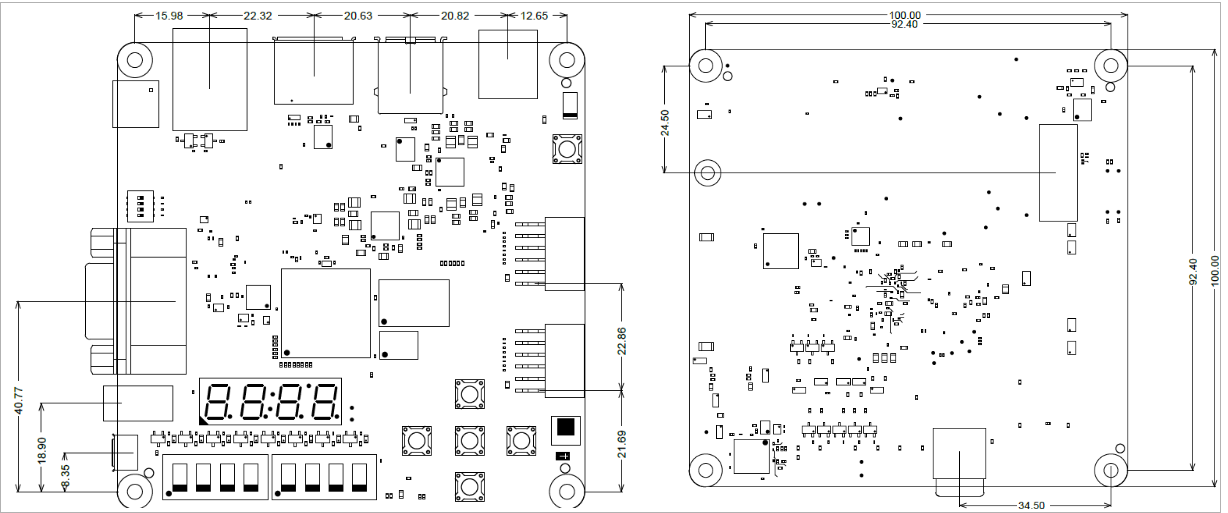 Image Added Image Added |
|
Currently Offered Variants
| Page properties |
|---|
|
Set correct link to the shop page overview table of the product on English and German. Example for TE0728: ENG Page: https://shop.trenz-electronic.de/en/Products/Trenz-Electronic/TE07XX-Zynq-SoC/TE0728-Zynq-SoC/ DEU Page: https://shop.trenz-electronic.de/de/Produkte/Trenz-Electronic/TE07XX-Zynq-SoC/TE0728-Zynq-SoC/ /TE0728-Zynq-SoC/ For Baseboards or modules, where no overview page is available (and revision number is coded in the direct link) use shop search link, e.g. TE0706: ENG Page: https://shop.trenz-electronic.de/en/search?sSearch=TE0706 DEU Page: https://shop.trenz-electronic.de/de/Produkte/Trenz-Electronic/TE07XX-Zynq-SoC/TE0728-Zynq-SoC/search?sSearch=TE0706 |
| Scroll Title |
|---|
| anchor | Table_VCP_SO |
|---|
| title | Trenz Electronic Shop Overview |
|---|
|
| Scroll Table Layout |
|---|
| orientation | portrait |
|---|
| sortDirection | ASC |
|---|
| repeatTableHeaders | default |
|---|
| sortByColumn | 1 |
|---|
| sortEnabled | false |
|---|
| cellHighlighting | true |
|---|
|
|
Revision History
Hardware Revision History
| Page properties |
|---|
|
Set correct links to download arrierFor Baseboards or modules, where no overview page is available (and revision number is coded in the direct link) use shop search link, e.g. TE0706 REV02: ENG Page: TE0706-02 -> https://shop.trenz-electronic.de/enDownload/search?sSearch=TE0706 DEU Page: https://shop.trenz-electronic.de/de/search?sSearch=TE0706path=Trenz_Electronic/Modules_and_Module_Carriers/4x5/4x5_Carriers/TE0706/REV02/Documents Note: |
| Scroll Title |
|---|
| anchor | Table_VCPRH_SOHRH |
|---|
| title | Trenz Electronic Shop Overview Hardware Revision History |
|---|
|
| Scroll Table Layout |
|---|
| orientation | portrait |
|---|
| sortDirection | ASC |
|---|
| repeatTableHeaders | default | style |
|---|
| widths | sortByColumn | 1 |
|---|
| sortEnabled | false |
|---|
| cellHighlighting | true |
|---|
|
|
| Trenz shop TE0728 overview page |
|---|
| English page | German page |
Revision History
Hardware Revision History
...
Set correct links to download arrier, e.g. TE0706 REV02:
TE0706-02 -> https://shop.trenz-electronic.de/Download/?path=Trenz_Electronic/Modules_and_Module_Carriers/4x5/4x5_Carriers/TE0706/REV02/Documents
Note:
| Date | Revision | Changes | Documentation Link |
|---|
| 2019-04-29 | 02 | - Added suppressor 1SMA5.0AT3G on power input
- Changed OV and UV protection range
- Changed VGA schematic
- USB page: VBUS resistor changed on 1K
| REV02 | | 2018-10-17 | 01 | Release | REV01 |
|
Hardware revision number can be found on the PCB board together with the module model number separated by the dash.
...
| Scroll Title |
|---|
| anchor | TableFigure_RHRV_HRHHRN |
|---|
| title | Board Hardware Revision HistoryNumber |
|---|
|
tablelayoutorientationportraitsortDirectionASCrepeatTableHeadersdefaultstyle | widths |
|---|
| sortByColumn | 1 |
|---|
| sortEnabled | false |
|---|
cellHighlightingDateRevisionChanges | Documentation Link | - |
Hardware revision number can be found on the PCB board together with the module model number separated by the dash.
| diagramName | TE0802_RV_HRN |
|---|
| simpleViewer | true |
|---|
| width | |
|---|
| links | auto |
|---|
| tbstyle | hidden |
|---|
| diagramWidth | 128 |
|---|
|
|
| Scroll Only |
|---|
 Image Added Image Added
|
|
| Scroll Title |
|---|
| anchor | Figure_RV_HRN |
|---|
| title | Board hardware revision number. |
|---|
|
| Scroll Ignore |
|---|
Create DrawIO object here: Attention if you copy from other page, objects are only linked. |
| Scroll Only |
|---|
image link to the generate DrawIO PNG file of this page. This is a workaround until scroll pdf export bug is fixed |
|
Document Change History
| Page properties |
|---|
|
- Note this list must be only updated, if the document is online on public doc!
- It's semi automatically, so do following
Add new row below first Copy "Page Information Macro(date)" Macro-Preview, Metadata Version number, Author Name and description to the empty row. Important Revision number must be the same as the Wiki document revision number Update Metadata = "Page Information Macro (current-version)" Preview+1 and add Author and change description. --> this point is will be deleted on newer pdf export template - Metadata is only used of compatibility of older exports
|
...
| Scroll Title |
|---|
| anchor | Table_RH_DCH |
|---|
| title | Document change history.Change History |
|---|
|
| Scroll Table Layout |
|---|
| orientation | portrait |
|---|
| sortDirection | ASC |
|---|
| repeatTableHeaders | default | style | widths |
|---|
| sortByColumn | 1 |
|---|
| sortEnabled | false |
|---|
| cellHighlighting | true |
|---|
|
| Date | Revision | Contributor | Description |
|---|
| Page info |
|---|
| infoType | Modified date |
|---|
| dateFormat | yyyy-MM-dd |
|---|
| type | Flat |
|---|
|
| | Page info |
|---|
| infoType | Current version |
|---|
| prefix | v. |
|---|
| type | Flat |
|---|
| showVersions | false |
|---|
|
| | Page info |
|---|
| infoType | Modified by |
|---|
| type | Flat |
|---|
| showVersions | false |
|---|
|
Initial Release | | | 2020-11-19 | v.65 | Pedram Babakhani | | -- | all | | Page info |
|---|
| infoType | Modified users |
|---|
| type | Flat |
|---|
| showVersions | false |
|---|
|
| |
|
...