...
| Scroll Title |
|---|
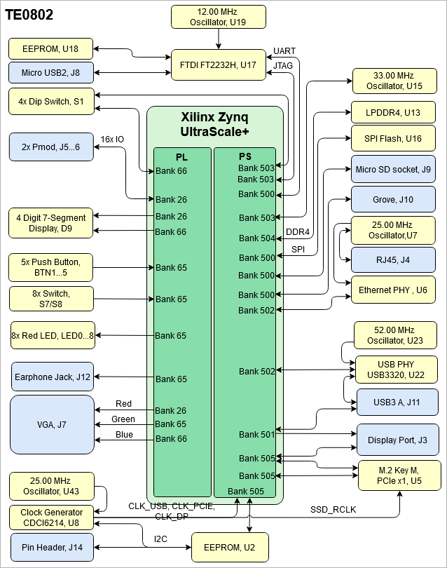
| anchor | Figure_OV_BD |
|---|
| title | TE0802 Block Diagram |
|---|
|
| Scroll Ignore |
|---|
| draw.io Diagram |
|---|
| border | false |
|---|
| viewerToolbar | true |
|---|
| |
|---|
| fitWindow | false |
|---|
| diagramDisplayName | |
|---|
| lbox | true |
|---|
| revision | 24 |
|---|
| diagramName | TE0802_OV_BD |
|---|
| simpleViewer | false |
|---|
| width | |
|---|
| links | auto |
|---|
| tbstyle | hidden |
|---|
| diagramWidth | 638 |
|---|
|
|
| Scroll Only |
|---|
|
|
...
Bootmode signals must be set through DIP Switch S9S1.
| Scroll Title |
|---|
| anchor | Table_OV_BP |
|---|
| title | Boot Process |
|---|
|
| Scroll Table Layout |
|---|
| orientation | portrait |
|---|
| sortDirection | ASC |
|---|
| repeatTableHeaders | default |
|---|
| sortByColumn | 1 |
|---|
| sortEnabled | false |
|---|
| cellHighlighting | true |
|---|
|
MODE Signal State | MODE1 S1-2(B) | MODE0 S1-1(A) | Boot Mode |
|---|
MODE[2:0]=000 | OFF | OFF | JTAG | MODE[2:0]=001 | OFF | ON | not supported | MODE[2:0]=010 | ON | OFF | QSPI(32 bit) | MODE[2:0]=011 | ON | ON | SD0(2.0) |
|
...
| Scroll Title |
|---|
| anchor | Table_OBP |
|---|
| title | On-board Peripherals |
|---|
|
| Scroll Table Layout |
|---|
| orientation | portrait |
|---|
| sortDirection | ASC |
|---|
| repeatTableHeaders | default |
|---|
| sortByColumn | 1 |
|---|
| sortEnabled | false |
|---|
| cellHighlighting | true |
|---|
|
|
Quad SPI Flash Memory
| Page properties |
|---|
|
Notes : Minimum and Maximum density of quad SPI flash must be mentioned for other assembly options. |
...
| Scroll Title |
|---|
| anchor | Table_OBP_DIP_SWITCH |
|---|
| title | DIP Switches |
|---|
|
| Scroll Table Layout |
|---|
| orientation | portrait |
|---|
| sortDirection | ASC |
|---|
| repeatTableHeaders | default |
|---|
| sortByColumn | 1 |
|---|
| sortEnabled | false |
|---|
| cellHighlighting | true |
|---|
|
| Designator | Schematic | Connected to | Functionality | Note |
|---|
| S1AS1-1(A) | MODE0 | Pin J16, FPGA Bank 503 | DIP | Pulled-down to GND. | | S1BS1-2(B) | MODE1 | Pin H15, FPGA Bank 503 | DIP | Pulled-down to GND. | | S1CS1-3(C) | USER_CFG0 | Pin A4, FPGA Bank 66 | DIP | Pulled-down to GND. | | S1DS1-4(D) | USER_CFG1 | Pin B4, FPGA Bank 66 | DIP | Pulled-down to GND. | | S7AS7-1(A) | USER_SW7 | Pin M5, FPGA Bank 65 | DIP | Pulled-up to +1.8V_PL. | | S7BS7-2(B) | USER_SW6 | Pin M4, FPGA Bank 65 | DIP | Pulled-up to +1.8V_PL. | | S7CS7-3(C) | USER_SW5 | Pin J2, FPGA Bank 65 | DIP | Pulled-up to +1.8V_PL. | | S7DS7-4(D) | USER_SW4 | Pin K1, FPGA Bank 65 | DIP | Pulled-up to +1.8V_PL. | | S8AS8-1(A) | USER_SW3 | Pin L1, FPGA Bank 65 | DIP | Pulled-up to +1.8V_PL. | | S8BS8-2(B) | USER_SW2 | Pin M1, FPGA Bank 65 | DIP | Pulled-up to +1.8V_PL. | | S8CS8-3(C) | USER_SW1 | Pin P2, FPGA Bank 65 | DIP | Pulled-up to +1.8V_PL. | | S8DS8-4(D) | USER_SW0 | Pin P3, FPGA Bank 65 | DIP | Pulled-up to +1.8V_PL. |
|
...
| Scroll Title |
|---|
| anchor | Table_RH_DCH |
|---|
| title | Document Change History |
|---|
|
| Scroll Table Layout |
|---|
| orientation | portrait |
|---|
| sortDirection | ASC |
|---|
| repeatTableHeaders | default |
|---|
| sortByColumn | 1 |
|---|
| sortEnabled | false |
|---|
| cellHighlighting | true |
|---|
|
| Date | Revision | Contributor | Description |
|---|
| Page info |
|---|
| infoType | Modified date |
|---|
| dateFormat | yyyy-MM-dd |
|---|
| type | Flat |
|---|
|
| | Page info |
|---|
| infoType | Current version |
|---|
| prefix | v. |
|---|
| type | Flat |
|---|
| showVersions | false |
|---|
|
| | Page info |
|---|
| infoType | Modified by |
|---|
| type | Flat |
|---|
| showVersions | false |
|---|
|
Technical Specifications updated | | | 2020-11-19 | v.65 | Pedram Babakhani | | -- | all | | Page info |
|---|
| infoType | Modified users |
|---|
| type | Flat |
|---|
| showVersions | false |
|---|
|
| |
|
...