...
- MPSoC: Xilinx Zynq XCZU2CG-1SBVA484E
- SDRAM: LPDDR4-3733 8Gb 256Mx32
- Storages:
- SPI Flash 256Mb (32M x 8) 133MHz
- microSD Card
- M.2 SSD PCIe
- Display Interfaces:
- DisplayPort
- VGA
- 4 Digit 7-Segment LED Display
- 8 LEDs
- Audio:
- Input:
- 5 User Buttons
- 8 Bit Slide Switches
- Reset Button
- User I/O:
- Communication:
- 1GB Ethernet RJ45
- USB Host 3.0 Host (Type A Connector)
- Debug
- Power
Block Diagram
| Page properties |
|---|
|
add drawIO object here.
|
...
| Scroll Title |
|---|
| anchor | Figure_OV_MC |
|---|
| title | TExxxx main componentsTE0802 Main Components (Picture shows Revision 01) |
|---|
|
| Scroll Ignore |
|---|
| draw.io Diagram |
|---|
| border | true |
|---|
| viewerToolbar | true |
|---|
| |
|---|
| fitWindow | false |
|---|
| diagramName | TE0802_OV_MC |
|---|
| simpleViewer | false |
|---|
| width | |
|---|
| diagramWidth | 610602 |
|---|
| revision | 78 |
|---|
|
|
| Scroll Only |
|---|
image link to the generate DrawIO PNG file of this page. This is a workaround until scroll pdf export bug is fixed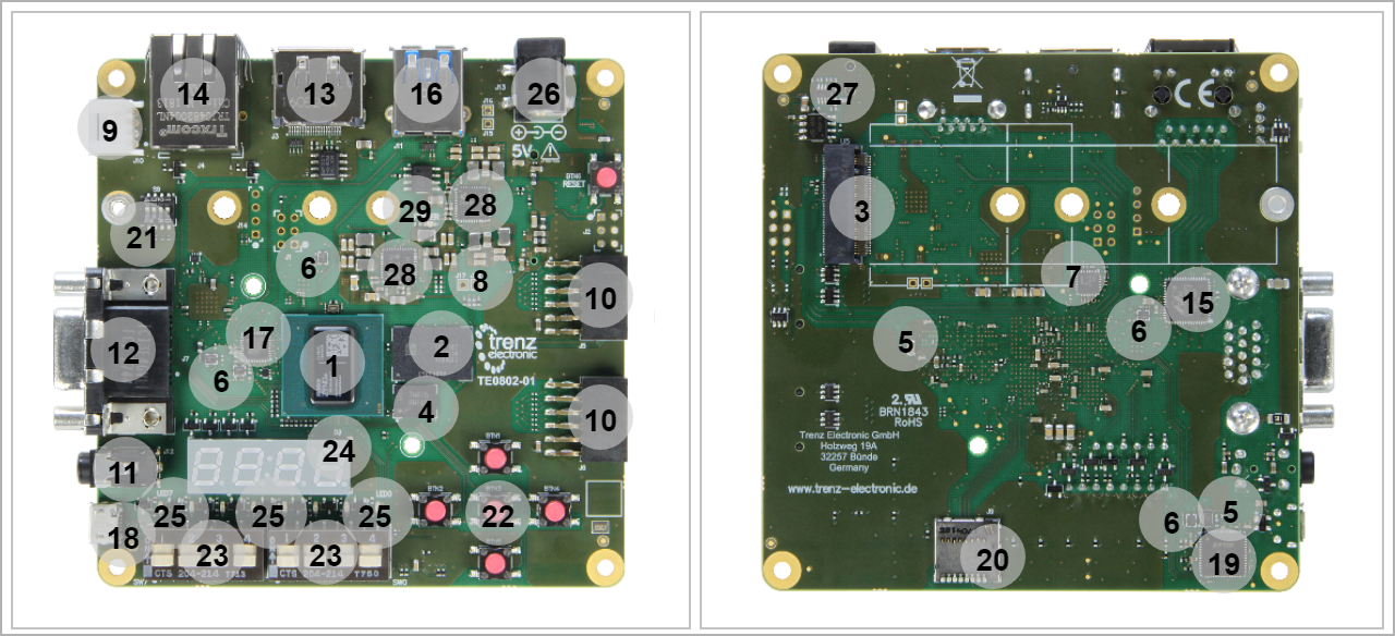 Image Added Image Added |
|
- Xilinx Zynq UltraScale+ MPSoc, U14
- LPDDR4 SDRAM, U13
- M.2 Key M PCIe x1, U5
- SPI Flash Memory, U16
- EEPROM, U2, U18
- Oscillator, U15, U7, U19, U23, U43
- Clock Generator, U8
- Clock Generator Programming Connector, J14
- Grove Connector, J10
- Pmod Host Socket, J5...6
- Headphone Jack, J12
- D-Sub Connector, J7
- DisplayPort, J3
- RJ45 Socket, J4
- Ethernet PHY, U6
- USB Type A, J11
- USB 2.0 PHY, U22
- Micro USB 2.0 Type B, J8
- FTDI USB 2.0 to JTAG/UART Converter, U17
- microSD Card, J9
- Slide Switch, S1
- Push Button, BTN1...5
- DIP Switch, S7...8
- 4 Digit 7-Segment LED Display, D9
- 8x LEDs (Red), LED0...7
- Power Jack, J13
- Overvoltage/Undervoltage/Reverse Supply Protector, U12
- Power Management Integrated Circuit (PMIC), U1, U9
- Power Good LED (Green), D12
...
| Scroll Title |
|---|
| anchor | Table_OV_IDS |
|---|
| title | Initial delivery state of programmable devices Delivery State of Programmable Devices on the moduleModule |
|---|
|
| Scroll Table Layout |
|---|
| orientation | portrait |
|---|
| sortDirection | ASC |
|---|
| repeatTableHeaders | default |
|---|
| style | |
|---|
| widths | |
|---|
| sortByColumn | 1 |
|---|
| sortEnabled | false |
|---|
| cellHighlighting | true |
|---|
|
Storage device name | Content | Notes |
|---|
Quad SPI Flash (U16) | Not programmed |
| | EEPROM (U2) | Not programmed | Except Ethernet MAC | | EEPROM (U18) | Programmed | FTDI Configuration | | LPDDR4 SDRAM (U13) | Not programmed | DDR3 SDRAM | System Controller CPLD |
|
|
Configuration Signals
| Page properties |
|---|
|
- Overview of Boot Mode, Reset, Enables.
|
...
| Page properties |
|---|
|
Notes : - For carrier or stand-alone boards use subsection for every connector type (add designator on description, not on the subsection title), for example:
- For modules which needs carrier use only classes and refer to B2B connector if more than one is used, for example
|
Board to Board (B2B) I/Os
JTAG Interface
JTAG access to the TExxxx SoM through B2B connector JMX.FPGA bank number and number of I/O signals connected to the B2B connector:
| Scroll Title |
|---|
| anchor | Table_SIP_B2BJTG |
|---|
| title | General PL I/O to B2B connectors informationJTAG pins connection |
|---|
|
| Scroll Table Layout |
|---|
| orientation | portrait |
|---|
| sortDirection | ASC |
|---|
| repeatTableHeaders | default |
|---|
| style | |
|---|
| widths | |
|---|
| sortByColumn | 1 |
|---|
| sortEnabled | false |
|---|
| cellHighlighting | true |
|---|
|
FPGA Bank| I/O Signal Count | Voltage Level | Notes | |
...
JTAG access to the TExxxx SoM through B2B connector JMX.
...
| anchor | Table_SIP_JTG |
|---|
| title | JTAG pins connection |
|---|
MIO Pins
| Page properties |
|---|
|
you must fill the table below with group of |
...
JTAG Signal
...
B2B Connector
...
MIO Pins
| Page properties |
|---|
|
you must fill the table below with group of MIOs which are connected to a specific components or peripherals, you do not have to specify pins in B2B, Just mention which B2B is connected to MIOs. The rest is clear in the Schematic. Example: | MIO Pin | Connected to | B2B | Notes |
|---|
| MIO12...14 | SPI_CS , SPI_DQ0... SPI_DQ3 SPI_SCK | J2 | QSPI |
|
...
Power supply with minimum current capability of xx 3 A for system startup is recommended.
...
| Scroll Title |
|---|
| anchor | Figure_PWR_PD |
|---|
| title | Power Distribution |
|---|
|
| Scroll Ignore |
|---|
| draw.io Diagram |
|---|
| border | true |
|---|
| viewerToolbar | true |
|---|
| |
|---|
| fitWindow | false |
|---|
| diagramName | TE0802_PWR_PD |
|---|
| simpleViewer | false |
|---|
| width | |
|---|
| diagramWidth | 561 |
|---|
| revision | 2 |
|---|
|
Create DrawIO object here: Attention if you copy from other page, objects are only linked. |
| Scroll Only |
|---|
image link to the generate DrawIO PNG file of this page. This is a workaround until scroll pdf export bug is fixed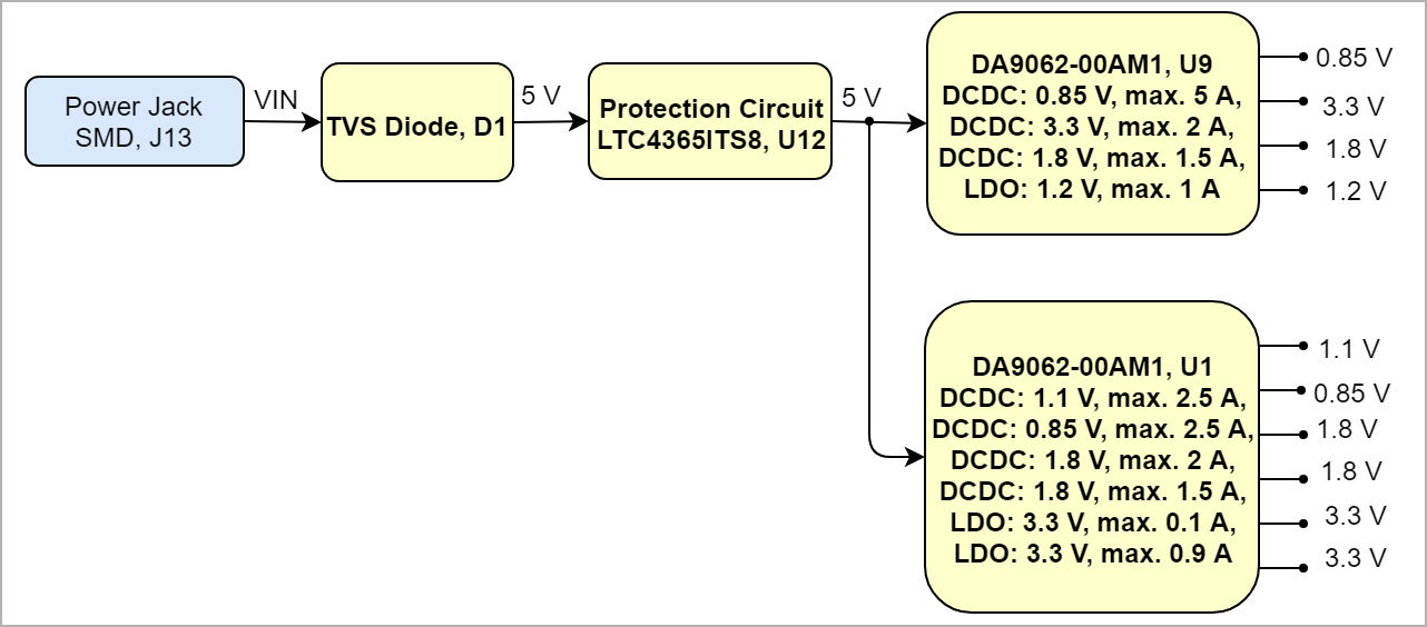 Image Added Image Added |
|
Power-On Sequence
| Scroll Title |
|---|
| anchor | Figure_PWR_PS |
|---|
| title | Power Sequency |
|---|
|
| Scroll Ignore |
|---|
Create DrawIO object here: Attention if you copy from other page, objects are only linked. |
| Scroll Only |
|---|
image link to the generate DrawIO PNG file of this page. This is a workaround until scroll pdf export bug is fixed |
|
...
Power Rails
| Scroll Title |
|---|
| anchor | FigureTable_PWR_VMCPR |
|---|
| title | Voltage Monitor CircuitModule power rails. |
|---|
|
| ignore |
Create DrawIO object here: Attention if you copy from other page, objects are only linked. |
| Scroll Only |
|---|
image link to the generate DrawIO PNG file of this page. This is a workaround until scroll pdf export bug is fixed |
Power Rails
| tablelayout |
|---|
| orientation | portrait |
|---|
| sortDirection | ASC |
|---|
| repeatTableHeaders | default |
|---|
| style | |
|---|
|
|
| Scroll Title |
|---|
| anchor | Table_PWR_PR |
|---|
| title | Module power rails. |
|---|
|
| Scroll Table Layout |
|---|
| orientation | portrait |
|---|
| sortDirection | ASC |
|---|
| repeatTableHeaders | default |
|---|
| style | widths | |
|---|
| sortByColumn | 1 |
|---|
| sortEnabled | false |
|---|
| cellHighlighting | true |
|---|
|
| Power Rail Name | B2B Connector JM1 Pin | B2B Connector JM2 Pin | B2B Connector JM3 Pin | Direction | Notes |
|---|
|
|
|
|
|
|
|
|
|
|
|
|
|
|
|
|
|
|
|
|
|
|
|
|
|
...
| Scroll Title |
|---|
| anchor | Table_PWR_BV |
|---|
| title | Zynq SoC bank voltages. |
|---|
|
| Scroll Table Layout |
|---|
| orientation | portrait |
|---|
| sortDirection | ASC |
|---|
| repeatTableHeaders | default |
|---|
| style | |
|---|
| widths | |
|---|
| sortByColumn | 1 |
|---|
| sortEnabled | false |
|---|
| cellHighlighting | true |
|---|
|
|
...
...
|
|---|
| Bank 503 | +3.3V | 3.3 V |
| | Bank 26 | +3.3V | 3.3 V |
| | Bank 65 | +1.8V_PL | 1.8 V |
| | Bank 500 | +3.3V | 3.3 V |
| | Bank 501 | +3.3V | 3.3 V |
| | Bank 502 | +1.8V_PS | 1.8 V |
| | Bank 504 | +1.1V_LPDDR4 | 1.1 V |
| | Bank 505 | +0.85V_MGTRAVCC +1.8V_MGTRAVTT | 0.85 V 1.8 V | ??? |
|
use "include page" macro and link to the general B2B connector page of the module series,
...
? x ? modules use two or three Samtec Micro Tiger Eye Connector on the bottom side.
3 x REF-??????? (compatible to ????????), (?? pins, ?? per row)
Operating Temperature: -??°C ~ ??°C
Current Rating: ??A per ContactNumber of Positions: ??
Number of Rows: ??
Technical Specifications
Absolute Maximum Ratings
| Scroll Title |
|---|
| anchor | Table_TS_AMR |
|---|
| title | PS absolute maximum ratings |
|---|
|
| Scroll Table Layout |
|---|
| orientation | portrait |
|---|
| sortDirection | ASC |
|---|
| repeatTableHeaders | default |
|---|
| style | |
|---|
| widths | |
|---|
| sortByColumn | 1 |
|---|
| sortEnabled | false |
|---|
| cellHighlighting | true |
|---|
|
| Symbols | Description | Min | Max | Unit |
|---|
| VIN | Input Supply Voltage (J13) | 4 | 5.5 | V | V | V | V | V | V | V | V |
|
Recommended Operating Conditions
...
| Scroll Title |
|---|
| anchor | Table_TS_ROC |
|---|
| title | Recommended operating conditions. |
|---|
|
| Scroll Table Layout |
|---|
| orientation | portrait |
|---|
| sortDirection | ASC |
|---|
| repeatTableHeaders | default |
|---|
| style | |
|---|
| widths | |
|---|
| sortByColumn | 1 |
|---|
| sortEnabled | false |
|---|
| cellHighlighting | true |
|---|
|
| Parameter | Min | Max | Units | Reference Document | V | See ???? datasheets. | V | See Xilinx ???? datasheet. | V | See Xilinx ???? datasheet. | V | See Xilinx ???? datasheet. | V | See Xilinx ???? datasheet. | V | See Xilinx ???? datasheet. | V | See Xilinx ???? datasheet. | °C | See Xilinx ???? datasheet. | °C | See Xilinx ???? datasheet. | | Max | Units | Reference Document |
|---|
| VIN | 4 | 5.5 | V |
|
|
Physical Dimensions
Module size:
...
100 mm ×
...
100 mm. Please download the assembly diagram for exact numbers.
...
Mating height with standard connectors: ? mm.
PCB thickness: ?? 1,48 mm.
| Page properties |
|---|
|
In 'Physical Dimension' section, top and bottom view of module must be inserted, information regarding physical dimensions can be obtained through webpage for product in Shop.Trenz, (Download> Documents> Assembly part) for every SoM. For Example: for Module TE0728, Physical Dimension information can be captured by snipping tools from the link below: https://www.trenz-electronic.de/fileadmin/docs/Trenz_Electronic/Modules_and_Module_Carriers/5.2x7.6/TE0745/REV02/Documents/AD-TE0745-02-30-1I.PDF
|
...
| Scroll Title |
|---|
| anchor | Table_RH_DCH |
|---|
| title | Document change history. |
|---|
|
| Scroll Table Layout |
|---|
| orientation | portrait |
|---|
| sortDirection | ASC |
|---|
| repeatTableHeaders | default |
|---|
| style | |
|---|
| widths | |
|---|
| sortByColumn | 1 |
|---|
| sortEnabled | false |
|---|
| cellHighlighting | true |
|---|
|
| Date | Revision | Contributor | Description |
|---|
| Page info |
|---|
| infoType | Modified date |
|---|
| dateFormat | yyyy-MM-dd |
|---|
| type | Flat |
|---|
|
| | Page info |
|---|
| infoType | Current version |
|---|
| prefix | v. |
|---|
| type | Flat |
|---|
| showVersions | false |
|---|
|
| | Page info |
|---|
| infoType | Modified by |
|---|
| type | Flat |
|---|
| showVersions | false |
|---|
|
| | -- | all | | Page info |
|---|
| infoType | Modified users |
|---|
| type | Flat |
|---|
| showVersions | false |
|---|
|
| |
|
...