...
TEI0802 is equipped with a Micro USB2.0 B connector J8 and a USB3.0 connector J11.
FTDI FT2232 (U17) can be accessed through Micro USB 2.0 B connector (J8) for JTAG (channel A). Channel B is connected to the FPGA and can be used for UART.
| Scroll Title |
|---|
| anchor | Table_SIP_USBUSB2 |
|---|
| title | USB USB2.0 B Socket Information |
|---|
|
| Scroll Table Layout |
|---|
| orientation | portrait |
|---|
| sortDirection | ASC |
|---|
| repeatTableHeaders | default |
|---|
| sortByColumn | 1 |
|---|
| sortEnabled | false |
|---|
| cellHighlighting | true |
|---|
|
| Corresponding Signals | USB0_D_N | USB0_DATA0...7 | MIO 52...63 FPGA Bank 502 | D+ | USB0_D_P | USB0_DATA0...7 | MIO 52...63 FPGA Bank 502 | StdA_SSRX- | USB_RX2_N | - | FPGA Bank 505 | | D_N | FTDI, U17 |
| | D+ | D_P | FTDI, U17 |
| | Vbus | USB_VBUS | GND |
StdA_SSRX+ | USB_RX2_P | - | FPGA Bank 505 | StdA_SSTX- | U3D2_N | USB_TX2_N | FPGA Bank 505 | StdA_SSTX+ | U3D2_P | USB_TX2_P | FPGA Bank 505
|
| Scroll Title |
|---|
| anchor | Table_SIP_USBUSB3 |
|---|
| title | USB USB3.0 A Socket Information |
|---|
|
| Scroll Table Layout |
|---|
| orientation | portrait |
|---|
| sortDirection | ASC |
|---|
| repeatTableHeaders | default |
|---|
| sortByColumn | 1 |
|---|
| sortEnabled | false |
|---|
| cellHighlighting | true |
|---|
|
Corresponding Signals | Connected to | Notes |
|---|
| D- | USB0_D_N | USB PHY, U22 |
| | D+ | USB0_D_P | USB PHY, U22 |
| | StdA_SSRX- | USB_RX2_N |
- | FPGA Bank 505 |
| | StdA_SSRX+ | USB_RX2_P |
-U3D2_N | | USB_TX2_N | FPGA Bank 505 |
| | StdA_SSTX+ |
U3D2_P | USB_TX2_P | FPGA Bank 505 |
| | VBUS | VBUS | USB PHY, U22 |
|
|
SSD M.2
TEI0802 is equipped with a SSD M.2 connector (U5).
...
| Scroll Title |
|---|
| anchor | Table_OBP |
|---|
| title | On-board Peripherals |
|---|
|
| Scroll Table Layout |
|---|
| orientation | portrait |
|---|
| sortDirection | ASC |
|---|
| repeatTableHeaders | default |
|---|
| sortByColumn | 1 |
|---|
| sortEnabled | false |
|---|
| cellHighlighting | true |
|---|
|
|
Quad SPI Flash Memory
| Page properties |
|---|
|
Notes : Minimum and Maximum density of quad SPI flash must be mentioned for other assembly options. |
...
| Scroll Title |
|---|
| anchor | Table_OBP_CLK_GEN |
|---|
| title | Clock Generator Connections and Pins |
|---|
|
| Scroll Table Layout |
|---|
| orientation | portrait |
|---|
| sortDirection | ASC |
|---|
| repeatTableHeaders | default |
|---|
| sortByColumn | 1 |
|---|
| sortEnabled | false |
|---|
| cellHighlighting | true |
|---|
|
| Clock Generator Pin | Signal Schematic Names | Connected to | Note |
|---|
| REFP | - | Pin 3, U43 (Oscillator) |
| | REFSEL | REFSEL | - | Pulled-up to +3.3V. | | RESETN/SYNC | CLK_GEN_RESET | Pin B5, FPGA Bank 26 | Pulled-up to +3.3V. | | EEPROMSEL | EEPROMSEL | - | Pulled-up to +3.3V. | | SDA/GPIO2 | CLK_GEN_SDA | - (Default) MIO9, FPGA Bank 500 (R185/196 required) Pin 2, J14 (Pin Header required) | Pulled-up to +3.3V. (Default) Pulled-up to +3.3V. Pulled-up to +3.3V. | | SCL/GPIO3 | CLK_GEN_SCL | - (Default) MIO8, FPGA Bank 500 (R185/196 required) Pin 3, J14 (Pin Header required) | Pulled-up to +3.3V. (Default) Pulled-up to +3.3V. Pulled-up to +3.3V. | | OE/GPIO4 | - | - | Pulled-up to +3.3V. | Y1P | CLK_Y1_P / CLK_DP_P | Pin G19, FPGA Bank 505 | 27 MHz | | Y1N | CLK_Y1_N / CLK_DP_N | Pin G20, FPGA Bank 505 | 27 MHz | Y2P | CLK_Y2_P / CLK_USB_P | Pin J19, FPGA Bank 505 | 26 MHz | | Y2N | CLK_Y2_N / CLK_USB_N | Pin J20, FPGA Bank 505 | 26 MHz | Y3P | CLK_Y3_P / CLK_PCIe_P | Pin L19, FPGA Bank 505 | 100 MHz | | Y3N | CLK_Y3_N / CLK_PCIe_N | Pin L20, FPGA Bank 505 | 100 MHz | Y4P | CLK_Y4_P / SSD_RCLK_P | Pin 55, U5 (M.2) | 100 MHz | | Y4N | CLK_Y4_N / SSD_RCLK_N | Pin 53, U5 (M.2) | 100 MHz |
|
...
Clock Sources
| Scroll Title |
|---|
| anchor | Table_OBP_CLK |
|---|
| title | Oscillators |
|---|
|
| Scroll Table Layout |
|---|
| orientation | portrait |
|---|
| sortDirection | ASC |
|---|
| repeatTableHeaders | default |
|---|
| sortByColumn | 1 |
|---|
| sortEnabled | false |
|---|
| cellHighlighting | true |
|---|
|
| Designator | Signal Schematic Names | Connected to | Description | Frequency | Note |
|---|
| U7 | ETH_XTAL_IN | Pin 34, U6 (Ethernet PHY) | Clock for Ethernet | 25 MHz |
| | U15 | PS_CLK | Pin H14, FPGA Bank 503 | Clock for FPGA | 33 MHz |
| | U23 | USB_CLK / USB0_RCLK | Pin 26, U22 (USB PHY) | Clock for USB | 52 MHz |
| | U43 | - | Pin 5, U8 (Clock Generator) | Clock for Clock Generator | 25 MHz |
|
|
...
| Scroll Title |
|---|
| anchor | Figure_PWR_PD |
|---|
| title | Power Distribution |
|---|
|
| Scroll Ignore |
|---|
| draw.io Diagram |
|---|
| border | false |
|---|
| viewerToolbar | true |
|---|
| |
|---|
| fitWindow | false |
|---|
| diagramDisplayName | |
|---|
| lbox | true |
|---|
| revision | 2 |
|---|
| diagramName | TE0802_PWR_PD |
|---|
| simpleViewer | true |
|---|
| width | |
|---|
| links | auto |
|---|
| tbstyle | hidden |
|---|
| diagramWidth | 561 |
|---|
|
|
| Scroll Only |
|---|
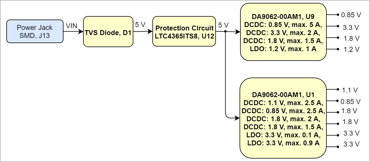 Image Modified Image Modified
|
|
Power-On Sequence
...
Module size: 100 mm × 100 mm. Please download the assembly diagram for exact numbers.
PCB thickness: 1,.48 mm
| Page properties |
|---|
|
In 'Physical Dimension' section, top and bottom view of module must be inserted, information regarding physical dimensions can be obtained through webpage for product in Shop.Trenz, (Download> Documents> Assembly part) for every SoM. For Example: for Module TE0728, Physical Dimension information can be captured by snipping tools from the link below: https://www.trenz-electronic.de/fileadmin/docs/Trenz_Electronic/Modules_and_Module_Carriers/5.2x7.6/TE0745/REV02/Documents/AD-TE0745-02-30-1I.PDF
|
...