...
| Scroll Title |
|---|
| anchor | Figure_OV_MC |
|---|
| title | TEBA0714 main components |
|---|
|
| Scroll Ignore |
|---|
| draw.io Diagram |
|---|
| border | false |
|---|
| viewerToolbar | true |
|---|
| |
|---|
| fitWindow | false |
|---|
| diagramDisplayName | |
|---|
| lbox | true |
|---|
| revision | 3 |
|---|
| diagramName | TEBA0714_OV_MC |
|---|
| simpleViewer | false |
|---|
| width | |
|---|
| links | auto |
|---|
| tbstyle | hidden |
|---|
| diagramWidth | 641 |
|---|
|
|
| Scroll Only |
|---|
|
|
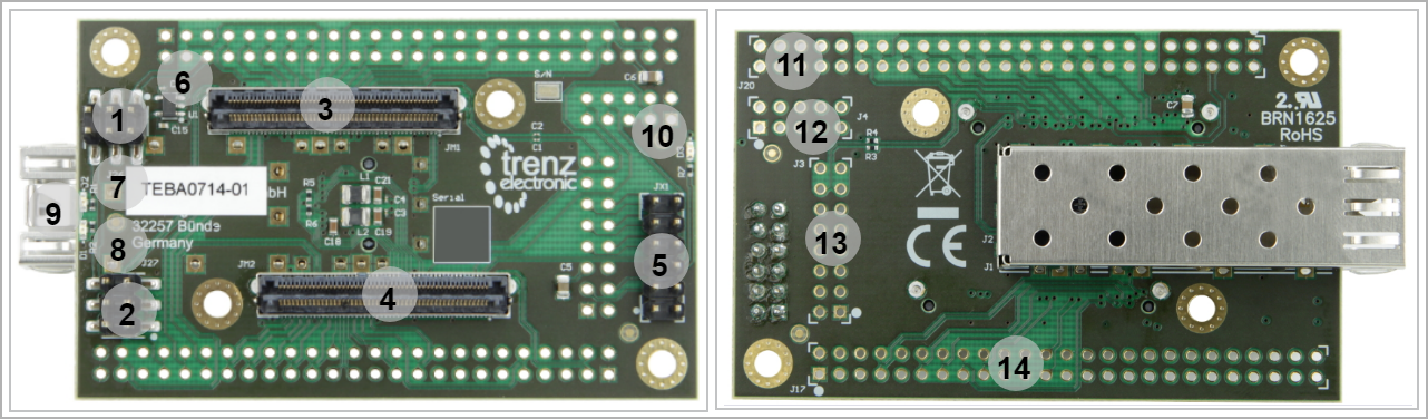
- 6-pin header J26 for selecting PL-bank I/O voltage
- 6-pin header J27 for selecting XMOD/JTAG VCCIO
- Samtec Razor Beam™ LSHM-150 B2B connector, JM1
- Samtec Razor Beam™ LSHM-150 B2B connector, JM2
- XMOD header, JX1
- Ultra small SMT coaxial connector, J5
- Ultra small SMT coaxial connector, J6
- Ultra small SMT coaxial connector, J7
- Ultra small SMT coaxial connector, J8
- User LED D1 (green)
- User LED D2 (red)
- LED D3 (red) indicating FPGA's 'Programming DONE'-signal
- SFP+ Connector, J1
- 10-pin header solder pads J4 for access to SoM's PL I/O-banks (LVDS pairs possible)
- 16-pin header solder pads J3, JTAG/UART header with ADC and MGT clock input
- 50-pin header solder pads J20 for access to SoM's PL I/O-banks (LVDS pairs possible)
- 50-pin header solder pads J17 for access to SoM's PL I/O-banks (LVDS pairs possible)
Initial Delivery State
| Page properties |
|---|
|
Notes : Only components like EEPROM, QSPI flash and DDR3 can be initialized by default at manufacture. If there is no components which might have initial data ( possible on carrier) you must keep the table empty |
- VCCIO voltage selection jumpers are all set to 1.8 V.
- Pin headers (not soldered to the board, but included in the package as separate component)
| Scroll Title |
|---|
| anchor | Table_OV_IDS |
|---|
| title | Initial delivery state of programmable devices on the module |
|---|
|
| Scroll Table Layout |
|---|
| orientation | portrait |
|---|
| sortDirection | ASC |
|---|
| repeatTableHeaders | default |
|---|
| style | |
|---|
| widths | |
|---|
| sortByColumn | 1 |
|---|
| sortEnabled | false |
|---|
| cellHighlighting | true |
|---|
|
Storage device name | Content | Notes |
|---|
- | - | - |
|
...
| Scroll Title |
|---|
| anchor | Table_SIP_B2B |
|---|
| title | General PL I/O to B2B connectors information |
|---|
|
| Scroll Table Layout |
|---|
| orientation | portrait |
|---|
| sortDirection | ASC |
|---|
| repeatTableHeaders | default |
|---|
| style | |
|---|
| widths | |
|---|
| sortByColumn | 1 |
|---|
| sortEnabled | false |
|---|
| cellHighlighting | true |
|---|
|
| B2B Connector | I/O Signal Count | Voltage Level | Notes |
|---|
| JM1 | User I/O | 54 single ended or 27 differential | - | | MGT lanes | 4 differential pairs, 2 lanes | - |
| | MGT reference clock input | 1 | - |
| | JTAG | 4 | - |
| | SoM control signals | 2 | 'PROG_B', 'DONE' |
| | ADC interface | 1 differential pair | - |
| | JM2 | User I/O | 36 single ended or 18 differential | - | | SFP+ Interface control signals | 8 | - |
| | QSPI interface | 6 | - |
| | UART interface | 2 | - |
| | User LEDs | 2 | Red, Green |
| | SoM control signals | 1 | 'BOOTMODE' | FPGA Bank | B2B Connector | I/O Signal Count | Voltage Level | Notes |
|
|---|
|
JTAG Interface
JTAG access to the TExxxx SoM through B2B connector JMX.
| Scroll Title |
|---|
| anchor | Table_SIP_JTG |
|---|
| title | JTAG pins connection |
|---|
|
| Scroll Table Layout |
|---|
| orientation | portrait |
|---|
| sortDirection | ASC |
|---|
| repeatTableHeaders | default |
|---|
| style | |
|---|
| widths | |
|---|
| sortByColumn | 1 |
|---|
| sortEnabled | false |
|---|
| cellHighlighting | true |
|---|
|
JTAG Signal | B2B Connector |
|---|
| TCK |
TMSTCK
|
MIO Pins
| Page properties |
|---|
|
you must fill the table below with group of MIOs which are connected to a specific components or peripherals, you do not have to specify pins in B2B, Just mention which B2B is connected to MIOs. The rest is clear in the Schematic. Example: | MIO Pin | Connected to | B2B | Notes |
|---|
| MIO12...14 | SPI_CS , SPI_DQ0... SPI_DQ3 SPI_SCK | J2 | QSPI |
|
...