Page History
...
| Scroll Title | ||||||||||||||||||||||||||||||||
|---|---|---|---|---|---|---|---|---|---|---|---|---|---|---|---|---|---|---|---|---|---|---|---|---|---|---|---|---|---|---|---|---|
| ||||||||||||||||||||||||||||||||
|
Main Components
...
| Scroll Title | ||||||||||||||||||||||||||||||||
|---|---|---|---|---|---|---|---|---|---|---|---|---|---|---|---|---|---|---|---|---|---|---|---|---|---|---|---|---|---|---|---|---|
| ||||||||||||||||||||||||||||||||
|
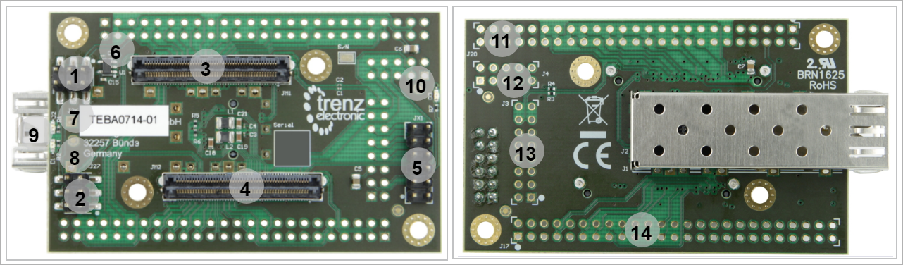
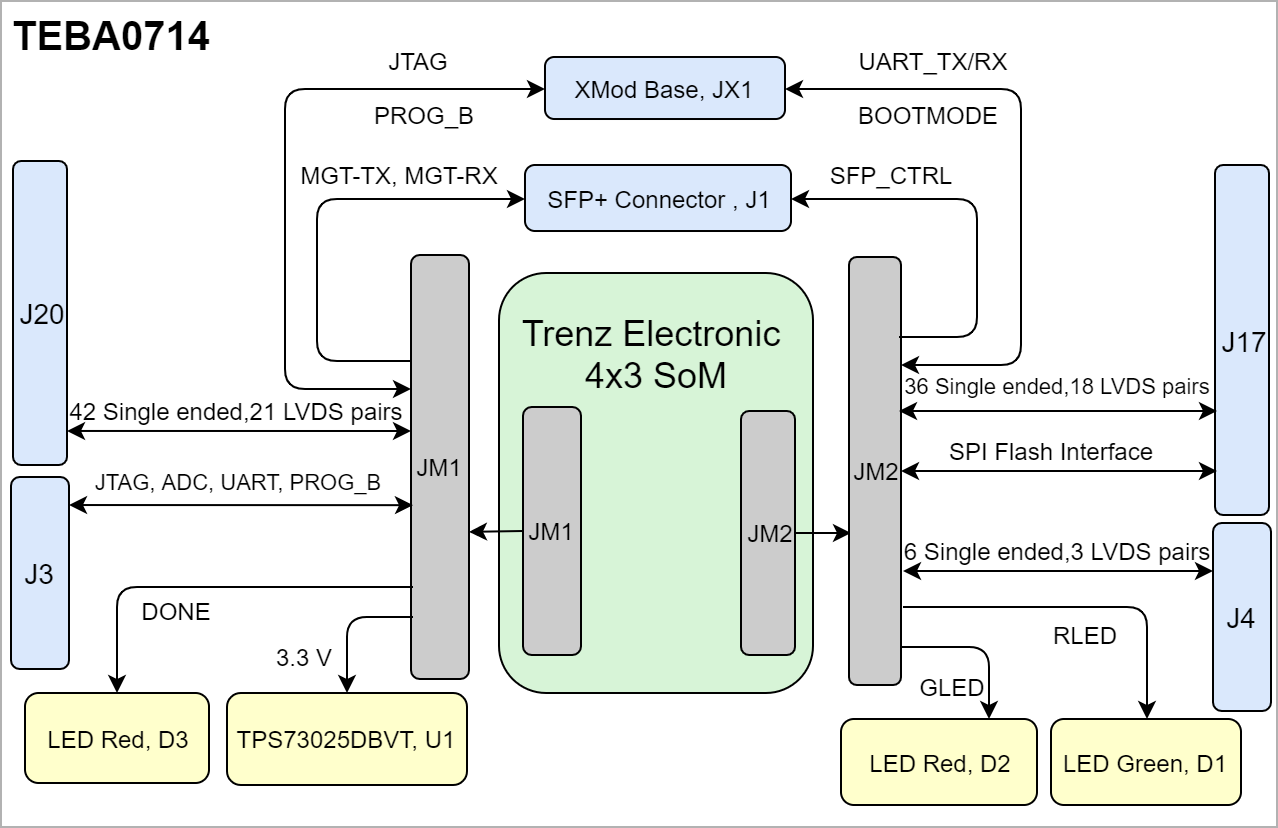
- 6-pin header J26 for selecting PL-bank I/O voltage
- 6-pin header J27 for selecting XMOD/JTAG VCCIO
- Samtec Razor Beam™ LSHM-150 B2B connector, JM1
- Samtec Razor Beam™ LSHM-150 B2B connector, JM2
- XMOD header, JX1
- Voltage Regulator, U1
- User Red LED D2
- User Green LED D1 (red)
- SFP+ Connector, J1
- Red LED D3, indicating FPGA's 'Programming DONE'-signal
- 1050-pin header solder pads J4 J20 for access to SoM's PL I/O-banks (LVDS pairs possible)
- 16-pin header solder pads J3, JTAG/UART header with ADC and MGT clock input
- 5010-pin header solder pads J20 J4 for access to SoM's PL I/O-banks (LVDS pairs possible)
- 50-pin header solder pads J17 for access to SoM's PL I/O-banks (LVDS pairs possible)
...
| Scroll Title | |||||||||||||||||||||||||||||
|---|---|---|---|---|---|---|---|---|---|---|---|---|---|---|---|---|---|---|---|---|---|---|---|---|---|---|---|---|---|
| |||||||||||||||||||||||||||||
|
| Scroll Title | ||||||||||||||||||||||||||||
|---|---|---|---|---|---|---|---|---|---|---|---|---|---|---|---|---|---|---|---|---|---|---|---|---|---|---|---|---|
| ||||||||||||||||||||||||||||
I/O |
|
Signals, Interfaces and Pins
...
Overview
Content Tools