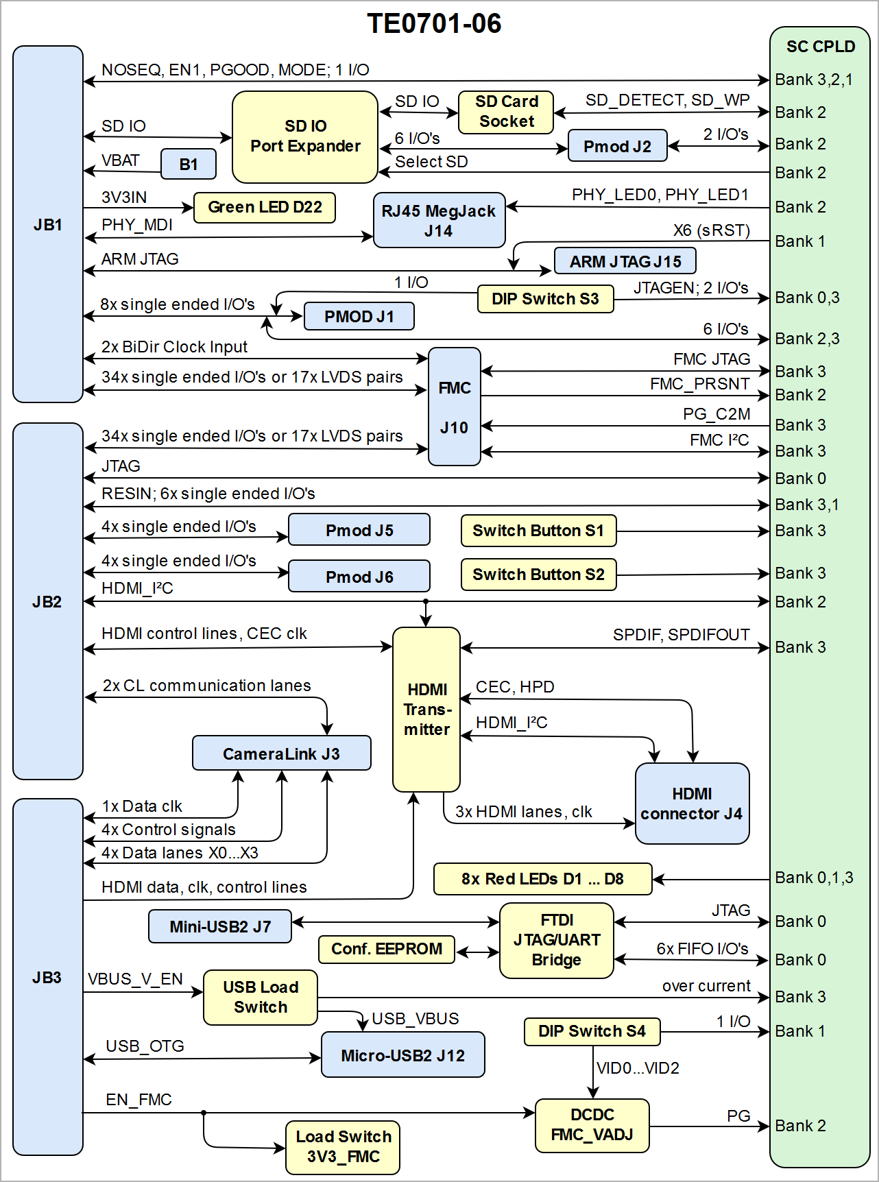
| SC CPLD U14 Pins and Interfaces | Connected to | Function | Notes |
|---|
| FMC_TMS | FMC J10, pin D31 | FMC JTAG | - |
| FMC_TDI | FMC J10, pin D29 |
| FMC_TDO | FMC J10, pin D30 |
| FMC_TCK | FMC J10, pin D33 |
| FMC_SDA | FMC J10, pin C31 | FMC I²C | - |
| FMC_SCL | FMC J10, pin C30 |
| PG_C2M | FMC J10, pin D1 | FMC control signals | - |
| FMC_PRSNT | FMC J10, pin H2 |
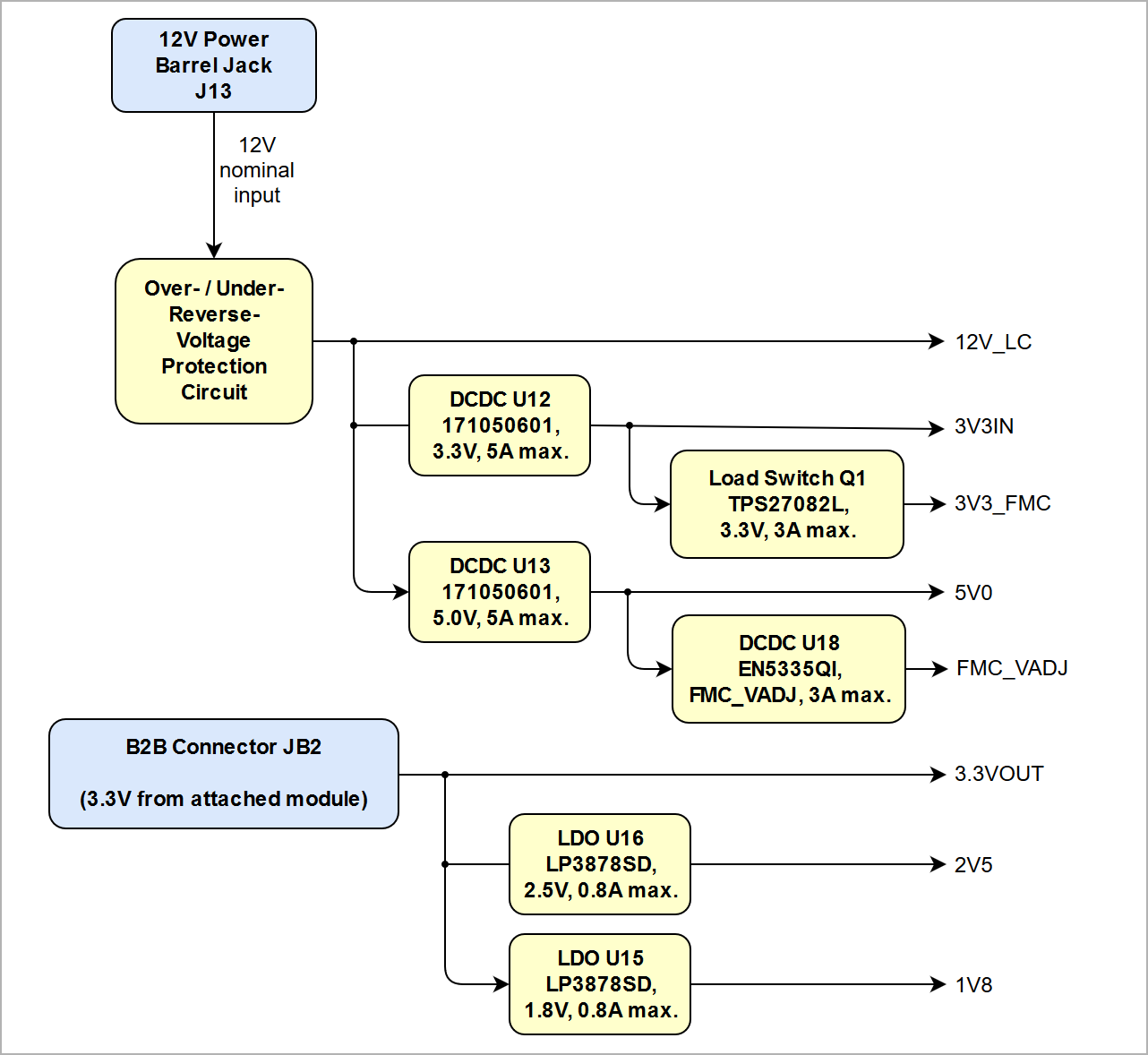
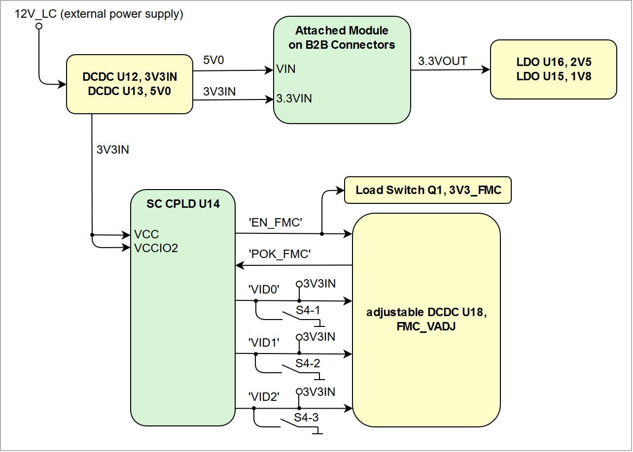
| EN_FMC | DC-DC U18, Load switch Q1 | FMC power control signals | - |
| POK_FMC | DC-DC U18 |
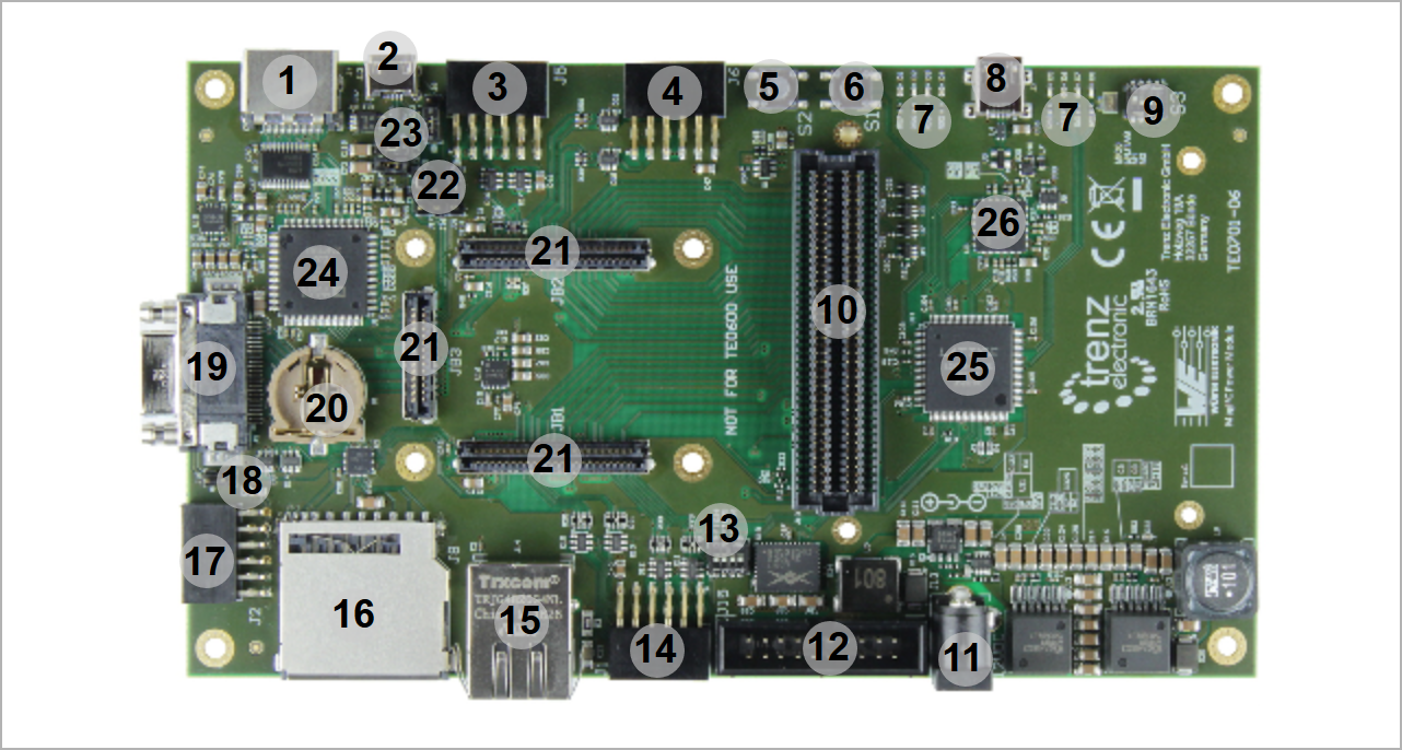
| S1 | Pushbutton S1 | available to user | - |
| S2 | Pushbutton S2 | Global Reset in standard configuration | - |
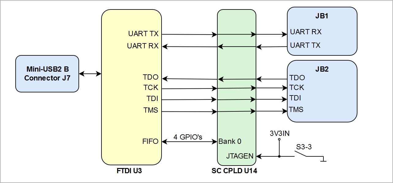
| M_TDO | FTDI chip, pin 14 (ADBUS2) | SC CPLD JTAG interface activated
if DIP switch S3-3 in OFF-position.
Attached module JTAG interface activated if
DIP switch S3-3 in ON-position. | - |
| M_TDI | FTDI chip, pin 13 (ADBUS1) |
| M_TCK | FTDI chip, pin 12 (ADBUS0) |
| M_TMS | FTDI chip, pin 15 (ADBUS3) |
| JTAGEN | DIP switch S3-3 |
| C_TMS | B2B JB2, pin 94 | Forwarded JTAG signals from FTDI chip,
if DIP switch S3-3 in ON-position. | JTAG signals
buffered with
ICs U4, U6,U7, U8 |
| C_TCK | B2B JB2, pin 100 |
| C_TDO | B2B JB2, pin 98 |
| C_TDI | B2B JB2, pin 96 |
| ADBUS4 | FTDI chip, pin 17 | FIFO / GPIO's available to user | - |
| ADBUS7 | FTDI chip, pin 20 |
| ACBUS4 | FTDI chip, pin 26 |
| ACBUS5 | FTDI chip, pin 27 |
| BDBUS0 | FTDI chip, pin 32 | UART TX from FTDI (forwarded to MIO14) | UART signals connected
to attached module |
| BDBUS1 | FTDI chip, pin 33 | UART RX to FTDI (forwarded from MIO15) |
| EN1 | B2B JB1, pin 27 | SoM control signals, functionalities depend
also on attached SoM's SC CPLD firmware. | - |
| NOSEQ | B2B JB1, pin 8 |
| PGOOD | B2B JB1, pin 29 |
| RESIN | B2B JB2, pin 17 |
| MODE | B2B JB1, pin 31 |
| ULED1 | Red LED D1 | USER LEDs, refer to the current firmware
documentation of the SC CPLD. | - |
| ULED2 | Red LED D2 |
| ULED3 | Red LED D3 |
| ULED4 | Red LED D4 |
| ULED5 | Red LED D5 |
| ULED6 | Red LED D6 |
| ULED7 | Red LED D7 |
| ULED8 | Red LED D8 |
| Y0 | B2B JB2, pin 42 | User I/O's between SC CPLD U14 and
attached module | - |
| Y1 | B2B JB2, pin 44 |
| Y2 | B2B JB2, pin 90 |
| Y3 | B2B JB2, pin 91 |
| Y4 | B2B JB2, pin 99 |
| Y5 | B2B JB2, pin 35 |
| Y6 | B2B JB1, pin 87 |
| X6 | B2B JB1, pin 99; ARM JTAG J15, pin 15 | ARM JTAG sRST (active low System Test Reset) | - |
| PHY_LED1 | RJ45 connector J14 | Current indicating function depends on
SC CPLD firmware. | - |
| PHY_LED2 |
| SEL_SD | SDIO port expander U2 | Control signal to select Port B0 or B1. | - |
| SD_DETECT | SD/MMC Card socket J8, pin 10 | Card Detect signal | - |
| SD_WP | SD/MMC Card socket J8, pin 11 | Write Protect signal |
| HDMI_SCL | HDMI Transmitter U1, pin 55 | HDMI transmitter 2-wire serial bus | - |
| HDMI_SDA | HDMI Transmitter U1, pin 56 |
| HDMI_SPDIFOUT | HDMI Transmitter U1, pin 46 | Unidirectional HDMI S/PDIF lines | - |
| HDMI_SPDIF | HDMI Transmitter U1, pin 10 |
| CM0 | DIP switch S3-2 | Set FMC_VADJ "S3-1 | S3-2: FMC_VADJ": OFF | OFF : 1.8V
OFF | ON : 2.5V
ON | OFF : 2.2V
ON | ON : I2C control enabled | DIP switch S4-1, S4-2 and S4-3
have to be set to OFF if use DIP
switches S3-1 and S3-2. |
| CM1 | DIP switch S3-1 |
| CM2 | DIP switch S4-4 | depends on current SC CPLD firmware | - |
| VID0 | DC-DC U18, pin 34; DIP switch S4-1 | set bit pattern as "VID2 | VID1 | VID0: FMC_VADJ":
0 | 0 | 0 : 3.3V
0 | 0 | 1 : 2.5V
0 | 1 | 0 : 1.8V
0 | 1 | 1 : 1.5V
1 | 0 | 0 : 1.25V
1 | 0 | 1 : 1.2V
1 | 1 | 0 : 0.8V (not supported as VCCIO standard)
1 | 1 | 1 : Reserved | SC CPLD settings will
be overridden by DIP switch
S4, if one of them is set to
one (OFF-position). |
| VID1 | DC-DC U18, pin 33; DIP switch S4-2 |
| VID2 | DC-DC U18, pin 32; DIP switch S4-3 |
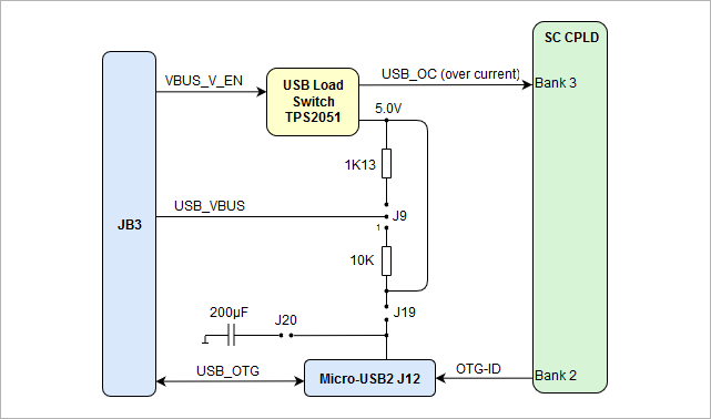
| USB_OC | USB-VBUS Load Switch U11, pin 5 | Indicates current threshold of USB devices exceeded. | low active logic |
| MIO10 | B2B JB1, pin 96; Pmod J1, pin 8 | User I/O's between SC CPLD U14, attached module
and Pmod connector J1. | - |
| MIO11 | B2B JB1, pin 94; Pmod J1, pin 9 |
| MIO12 | B2B JB1, pin 100; Pmod J1, pin 10 |
| MIO13 | B2B JB1, pin 98; Pmod J1, pin 7 |
| MIO14 | B2B JB1, pin 91; Pmod J1, pin 3 | UART interface in standard SC CPLD firmware, else
user I/O's. |
| MIO15 | B2B JB1, pin 86; Pmod J1, pin 4 |
| PX6 | Pmod J2, pin 9 | User I/O's of SC CPLD U14 | - |
| PX7 | Pmod J2, pin 10 |
| VCCIO0 | 3V3IN | VCCIO SC CPLD bank 0 | - |
| VCCIO1 | VIOTB | VCCIO SC CPLD bank 1 | adjustable voltage, see section 'Power' |
| VCCIO2 | 3V3IN | VCCIO SC CPLD bank 2 | - |
| VCCIO3 | 3V3IN | VCCIO SC CPLD bank 3 | - |