...
| Scroll Title |
|---|
| anchor | Figure_OV_MC |
|---|
| title | TEF0003 main components |
|---|
|
| Scroll Ignore |
|---|
| draw.io Diagram |
|---|
| border | false |
|---|
| viewerToolbar | true |
|---|
| |
|---|
| fitWindow | false |
|---|
| diagramDisplayName | |
|---|
| lbox | true |
|---|
| revision | 7 |
|---|
| diagramName | TEF0003_OV_MC |
|---|
| simpleViewer | false |
|---|
| width | |
|---|
| links | auto |
|---|
| tbstyle | hidden |
|---|
| diagramWidth | 641 |
|---|
|
|
| Scroll Only |
|---|
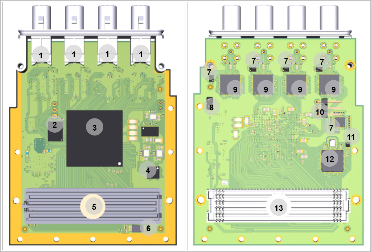 Image Modified Image Modified
|
|
- Coaxial Connectors, J2-5
- SPI Flash, U9
- Xilinx Artix 7 FPGA, U1
- Lattice MachXO FPGA, U15
- Vita 57 Connector, J1
- EEPROM, U4
- I2C Switches, U2, U17-20
- Jumper, J7
- Serializer, U5-8
- Connector Header, J8
- Oscillator 25MHz, U11
- Programmable Clock Generator, U10
- Vita 57 Connector, J6
...
There is a Silicon Labs I2C programmable clock generator on-board (U10) to generate reference clocks for the module. Programming can be done using I2C via PIN header J8. The I2C Address is 0x69.
| Scroll Title |
|---|
| anchor | Table_OBP_PCLK |
|---|
| title | Programmable Clock Generator Inputs and Outputs |
|---|
|
| Scroll Table Layout |
|---|
| orientation | portrait |
|---|
| sortDirection | ASC |
|---|
| repeatTableHeaders | default |
|---|
| sortByColumn | 1 |
|---|
| sortEnabled | false |
|---|
| cellHighlighting | true |
|---|
|
Si5345A Pin
| Signal Name / Description
| Connected To | Direction | Note |
|---|
IN0 | Reference input clock. | U11 | Input | 25.00 MHz oscillator, SiT8008BI | | IN1 | FMCT_GBTCLK0 | J6E | Input | Vita 57 Connector | | IN2 | FMCT_GBTCLK1 | J6E | Input | Vita 57 Connector | | IN3 | FMCT_CLK0 | J6E | Input | Vita 57 Connector | XAXB | - | GND | Input | 54.0000 MHz XTAL CX3225SB | | SCLK | PLL_SCL | J8, U20 | Input | EEPROM Programming | | SDA | PLL_SDA | J8, U20 | Input | EEPROM Programming | | OUT0 | GA_PCLK | U5/U1 | Output | FPGA bank 15 | | OUT1 | GB_PCLK | U6/U1 | Output | FPGA bank 15 | | OUT2 | GC_PCLK | U7/U1 | Output | FPGA bank 15 | | OUT3 | GD_PCLK | U8/U1 | Output | FPGA bank 15 | | OUT4 | CLK4_P | U1H | Output |
| | OUT5 | GBTCLK0 | J1E/J6E | Output |
| | OUT6 | GBTCLK1 | J1E/J6E | Output |
| | OUT7 | GBTCLK0 | J1E | Output |
| | OUT8 | CLK8 | Not Conneted | Output | Not Used | | OUT9 | CLK9 | Not Conneted | Output | Not Used |
|
...
| Scroll Title |
|---|
| anchor | Figure_PWR_PS |
|---|
| title | Power Sequency |
|---|
|
| Scroll Ignore |
|---|
| draw.io Diagram |
|---|
| border | false |
|---|
| viewerToolbar | true |
|---|
| |
|---|
| fitWindow | false |
|---|
| diagramDisplayName | |
|---|
| lbox | true |
|---|
| revision | 1 |
|---|
| diagramName | TEF0003_PWR_PS |
|---|
| simpleViewer | false |
|---|
| width | |
|---|
| links | auto |
|---|
| tbstyle | hidden |
|---|
| diagramWidth | 641 |
|---|
|
|
| Scroll Only |
|---|
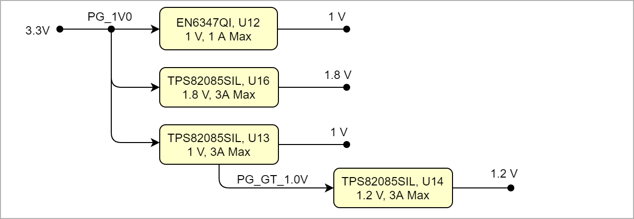 Image Modified Image Modified
|
|
Power Rails
| Scroll Title |
|---|
| anchor | Table_PWR_PR |
|---|
| title | Module power rails. |
|---|
|
| Scroll Table Layout |
|---|
| orientation | portrait |
|---|
| sortDirection | ASC |
|---|
| repeatTableHeaders | default |
|---|
| sortByColumn | 1 |
|---|
| sortEnabled | false |
|---|
| cellHighlighting | true |
|---|
|
B2B JM1 PinB2B JM2 Pin B2B Connector JM3 Pin | |
Bank Voltages
...
| anchor | Table_PWR_BV |
|---|
| title | Zynq SoC bank voltages. |
|---|
| Scroll Table Layout |
|---|
| orientation | portrait |
|---|
| sortDirection | ASC |
|---|
| repeatTableHeaders | default |
|---|
| sortByColumn | 1 |
|---|
| sortEnabled | false |
|---|
| cellHighlighting | true |
|---|
|
...
...
...
| 12V | C35, C37 | C35, C37 | Input |
| | 3P3VAUX | D32 | D32 | Input |
| | 3P3V | D36, D38, D40, C39 | D36, D38, D40, C39 | Input |
| VREFA | H1 | H1 | Input |
| | VREFB | K1 | K1 | Input |
| | VIOB | J39, K40 | J39, K40 | Input |
| | VADJ | H40, G39, F40, E39 | H40, G39, F40, E39 | Input |
|
|
Bank Voltages
| Scroll Title |
|---|
| anchor | Table_PWR_BV |
|---|
| title | Zynq SoC bank voltages. |
|---|
|
| Scroll Table Layout |
|---|
| orientation | portrait |
|---|
| sortDirection | ASC |
|---|
| repeatTableHeaders | default |
|---|
| sortByColumn | 1 |
|---|
| sortEnabled | false |
|---|
| cellHighlighting | true |
|---|
|
| Schematic Name | | Notes |
|---|
| Bank 13 | VCCO_13 | 1.8 V |
| | Bank 14 | VCCO_14 | 1.8 V |
| | Bank 15 | VCCO_15 | 1.8 V |
| | Bank 16 | VCCO_16 | VADJ |
| | Bank 34 | VCCO_34 | 1.8 V |
| | Bank 34 | VCCO_35 | VADJ |
| | Bank 0 | VCCO_0 | 1.8 V |
|
|
Board to Board Connectors
| Page properties |
|---|
|
- This section is optional and only for modules.
|
| Page properties |
|---|
|
- This section is optional and only for modules.
use "include page" macro and link to the general B2B connector page of the module series, For example: 6 x 6 SoM LSHM B2B Connectors
| Include Page |
|---|
| PD:6 x 6 SoM LSHM B2B Connectors |
|---|
| PD:6 x 6 SoM LSHM B2B Connectors |
|---|
|
|
...
| Scroll Title |
|---|
| anchor | Table_TS_AMR |
|---|
| title | PS absolute maximum ratings |
|---|
|
| Scroll Table Layout |
|---|
| orientation | portrait |
|---|
| sortDirection | ASC |
|---|
| repeatTableHeaders | default |
|---|
| sortByColumn | 1 |
|---|
| sortEnabled | false |
|---|
| cellHighlighting | true |
|---|
|
| Symbols | Description | Min | Max | Unit |
|---|
VVV | V | V | V | V | | T_STG | Storage Temperature |
|
| °C |
|
Recommended Operating Conditions
...
| Scroll Title |
|---|
| anchor | Table_TS_ROC |
|---|
| title | Recommended operating conditions. |
|---|
|
| Scroll Table Layout |
|---|
| orientation | portrait |
|---|
| sortDirection | ASC |
|---|
| repeatTableHeaders | default |
|---|
| sortByColumn | 1 |
|---|
| sortEnabled | false |
|---|
| cellHighlighting | true |
|---|
| | repeatTableHeaders | default |
|---|
| sortByColumn | 1 |
|---|
| sortEnabled | false |
|---|
| cellHighlighting | true |
|---|
|
| Parameter | Min | Max | Units | Reference Document |
|---|
|
|
| V | See ???? datasheets | | Parameter | Min | Max | Units | Reference Document |
|---|
| V | See ???? datasheets. | V | See Xilinx ???? datasheet. | V | See Xilinx ???? datasheet. | V | See Xilinx ???? datasheet. | V | See Xilinx ???? datasheet. | V | See Xilinx ???? datasheet. | V | See Xilinx ???? datasheet. | °C | See Xilinx ???? datasheet. |
|
|
| °C | See Xilinx ???? datasheet. |
|
...