...
| Page properties |
|---|
|
Note for Download Link of the Scroll ignore macro: |
| Scroll pdf ignore |
|---|
Table of Contents |
...
| Page properties |
|---|
|
Note:
'description: Important components and connector or other Features of the module
→ please sort and indicate assembly options Key Features' must be split into 6 main groups: - FPGA/Module
- Package:
- Speed:
- Temperature:
- RAM/Storage
- On Board
- Interface
- E.g. ETH, USB, B2B, Display port
- Power
- E.g. Input supply voltage
- Dimension
|
- FPGA: Xilinx Artix 7 (XC7A100T)
- Package: FGG484 (Compatible with
- Speed: -1 (Slowest)
- Temperature: Industrial Grade (–40°C to +100°C)
- RAM/Storage:
- 1x NOR SPI FLASH (128M x 4)
- 1x EEPROM (16K x 8)
- On Board:
- 4x Deserializer IC (3.12 Gbps)
- 4x I2C and SMBus I/O Expander
- 1x Programable Clock Generator
- 1x Clock Generator
- Interface:
- 2x VITA 57 SEAM/SEAF Series
- 4x Coaxial Connectors
- Power:
- 4x Voltage Regulators
- 3.3 Supply Voltage
- Dimension: 72 mm x 65 mm
Block Diagram
...
| Scroll Title |
|---|
| anchor | Figure_OV_BD |
|---|
| title | TEF0003 block diagram |
|---|
|
| Scroll Ignore |
|---|
| draw.io Diagram |
|---|
| border | false |
|---|
| viewerToolbar | true |
|---|
| |
|---|
| fitWindow | false |
|---|
| diagramDisplayName | |
|---|
| lbox | true |
|---|
| revision | 910 |
|---|
| diagramName | TEF0003_OV_BD |
|---|
| simpleViewer | false |
|---|
| width | |
|---|
| links | auto |
|---|
| tbstyle | hidden |
|---|
| diagramWidth | 641 |
|---|
|
|
| Scroll Only |
|---|
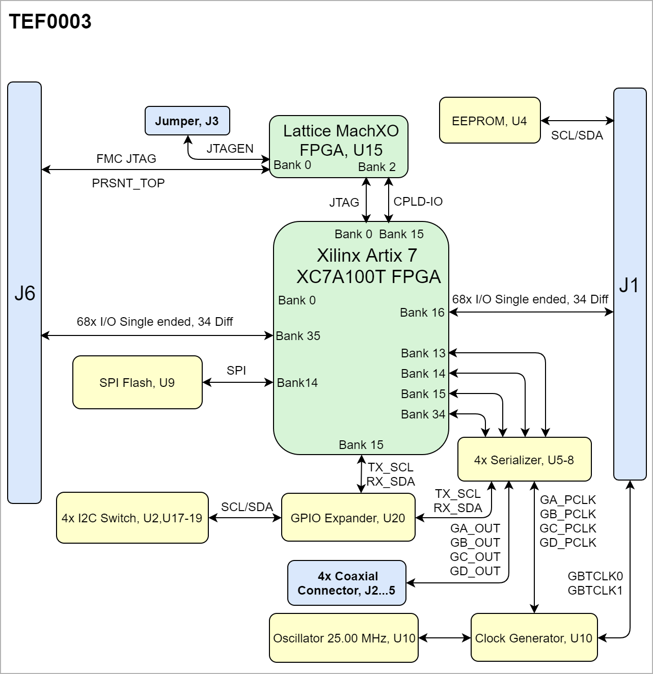 Image Modified Image Modified
|
|
Main Components
...
| Scroll Title |
|---|
| anchor | Table_OV_RST |
|---|
| title | Reset Process. |
|---|
|
| Scroll Table Layout |
|---|
| orientation | portrait |
|---|
| sortDirection | ASC |
|---|
| repeatTableHeaders | default |
|---|
| sortByColumn | 1 |
|---|
| sortEnabled | false |
|---|
| cellHighlighting | true |
|---|
|
Signal | Description | Note |
|---|
PRSNT_TOP | Lattice MachXO Configuration Pin |
| | PROG_B | Artix 7 Configuration Pin | , Connected to 1.8 |
|
Signals, Interfaces and Pins
...
| Scroll Title |
|---|
| anchor | Table_OBP |
|---|
| title | On board peripherals |
|---|
|
| Scroll Table Layout |
|---|
| orientation | portrait |
|---|
| sortDirection | ASC |
|---|
| repeatTableHeaders | default |
|---|
| sortByColumn | 1 |
|---|
| sortEnabled | false |
|---|
| cellHighlighting | true |
|---|
|
|
Quad SPI Flash Memory
...
| Scroll Title |
|---|
| anchor | Table_OBP_CLK |
|---|
| title | Osillators |
|---|
|
| Scroll Table Layout |
|---|
| orientation | portrait |
|---|
| sortDirection | ASC |
|---|
| repeatTableHeaders | default |
|---|
| sortByColumn | 1 |
|---|
| sortEnabled | false |
|---|
| cellHighlighting | true |
|---|
|
| Designator | Description | Frequency | Note |
|---|
| U4 | Oscillator | , 25 MHz | MHz |
| | U10 | Programmable Clock Generator | MHzVariable |
|
|
Programmable Clock Generator
...
| Scroll Title |
|---|
| anchor | Table_OBP_PCLK |
|---|
| title | Programmable Clock Generator Inputs and Outputs |
|---|
|
| Scroll Table Layout |
|---|
| orientation | portrait |
|---|
| sortDirection | ASC |
|---|
| repeatTableHeaders | default |
|---|
| sortByColumn | 1 |
|---|
| sortEnabled | false |
|---|
| cellHighlighting | true |
|---|
|
Si5345A Pin
| Signal Name / Description
| Connected To | Direction | Note |
|---|
IN0 | Reference input clock. | U11 | Input | 25.00 MHz oscillator, SiT8008BI | | IN1 | FMCT_GBTCLK0 | J6E | Input | FMC Pcam Adapter | | IN2 | FMCT_GBTCLK1 | J6E | Input | FMC Pcam Adapter | | IN3 | FMCT_CLK0 | J6E | Input | FMC Pcam Adapter | XAXB | - | GND | Input | 54.0000 MHz XTAL CX3225SB | | SCLK | PLL_SCL | J8, U20 | Input | EEPROM Programming | | SDA | PLL_SDA | J8, U20 | Input | EEPROM Programming | | OUT0 | GA_PCLK | U5/U1 | Output | FPGA bank 15 | | OUT1 | GB_PCLK | U6/U1 | Output | FPGA bank 15 | | OUT2 | GC_PCLK | U7/U1 | Output | FPGA bank 15 | | OUT3 | GD_PCLK | U8/U1 | Output | FPGA bank 15 | | OUT4 | CLK4_P | U1H | Output |
| | OUT5 | GBTCLK0 | J1E/J6E | Output |
| | OUT6 | GBTCLK1 | J1E/J6E | Output |
| | OUT7 | GBTCLK0 | J1E | Output |
| | OUT8/OUT9 | CLK8/CLK9 | Not ConnetedPulled low | OutputNot Used |
|
|
Power and Power-On Sequence
...
| Scroll Title |
|---|
| anchor | Table_PWR_PR |
|---|
| title | Module power rails. |
|---|
|
| Scroll Table Layout |
|---|
| orientation | portrait |
|---|
| sortDirection | ASC |
|---|
| repeatTableHeaders | default |
|---|
| sortByColumn | 1 |
|---|
| sortEnabled | false |
|---|
| cellHighlighting | true |
|---|
|
| Power Rail Name | FMC Adapter J1G Pin | FMC Adapter J6G Pin | Direction | Notes |
|---|
| 12V | C35, C37 | C35, C37 | Input |
| | 3P3VAUX | D32 | D32 | Input |
| | 3P3V | D36, D38, D40, C39 | D36, D38, D40, C39 | Input |
| VREFA | H1 | H1 | Input |
| | VREFB | K1 | K1 | Input |
| | VIOB | J39, K40 | J39, K40 | Input |
| | VADJ | H40, G39, F40, E39 | H40, G39, F40, E39 | Input |
|
|
...
| Scroll Title |
|---|
| anchor | Table_PWR_BV |
|---|
| title | Zynq SoC bank voltages. |
|---|
|
| Scroll Table Layout |
|---|
| orientation | portrait |
|---|
| sortDirection | ASC |
|---|
| repeatTableHeaders | default |
|---|
| sortByColumn | 1 |
|---|
| sortEnabled | false |
|---|
| cellHighlighting | true |
|---|
|
| Schematic Name | | Notes |
|---|
| Bank 13 | VCCO_13 | 1.8 V |
| | Bank 14 | VCCO_14 | 1.8 V |
| | Bank 15 | VCCO_15 | 1.8 V |
| | Bank 16 | VCCO_16 | VADJ | 1.8 V | | Bank 34 | VCCO_34 | 1.8 V |
| | Bank 35 | VCCO_35 | VADJ | 1.8 V | | Bank 0 | VCCO_0 | 1.8 V |
|
Board to Board Connectors
| Page properties |
|---|
|
| This section is optional and only for modules. use "include page" macro and link to the general B2B connector page of the module series, For example: 6 x 6 SoM LSHM B2B Connectors
include | PD:6 x 6 SoM LSHM B2B Connectors | PD:6 x 6 SoM LSHM B2B Connectors |
Technical Specifications
Absolute Maximum Ratings
...
Module size: 84 mm × 65 mm. Please download the assembly diagram for exact numbers.
Mating height with standard connectors: 10 mm.
PCB thickness: 1.54 56 mm.
| Page properties |
|---|
|
In 'Physical Dimension' section, top and bottom view of module must be inserted, information regarding physical dimensions can be obtained through webpage for product in Shop.Trenz, (Download> Documents> Assembly part) for every SoM. For Example: for Module TE0728, Physical Dimension information can be captured by snipping tools from the link below: https://www.trenz-electronic.de/fileadmin/docs/Trenz_Electronic/Modules_and_Module_Carriers/5.2x7.6/TE0745/REV02/Documents/AD-TE0745-02-30-1I.PDF
|
...
| Scroll Title |
|---|
| anchor | Table_VCP_SO |
|---|
| title | Trenz Electronic Shop Overview |
|---|
|
| Scroll Table Layout |
|---|
| orientation | portrait |
|---|
| sortDirection | ASC |
|---|
| repeatTableHeaders | default |
|---|
| sortByColumn | 1 |
|---|
| sortEnabled | false |
|---|
| cellHighlighting | true |
|---|
|
|
Revision History
Hardware Revision History
...