| Scroll Table Layout |
|---|
| orientation | portrait |
|---|
| sortDirection | ASC |
|---|
| repeatTableHeaders | default |
|---|
| style | |
|---|
| widths | |
|---|
| sortByColumn | 1 |
|---|
| sortEnabled | false |
|---|
| cellHighlighting | true |
|---|
|
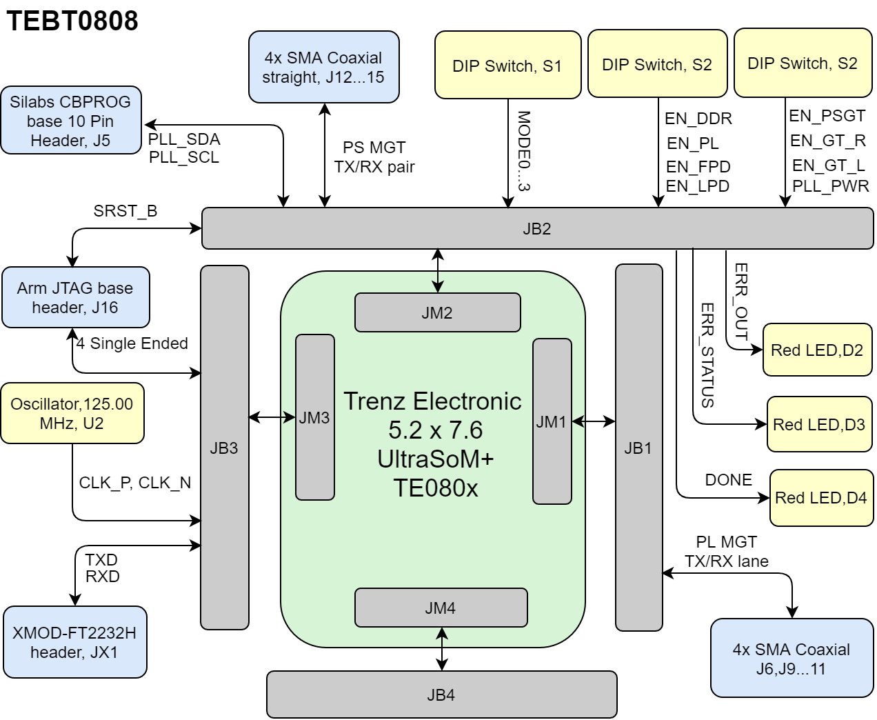
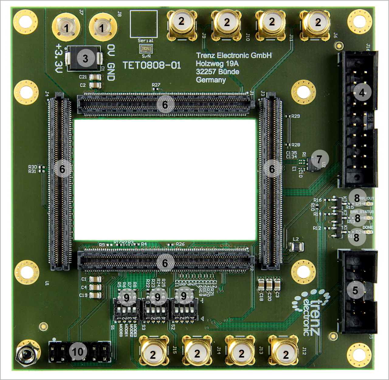
| B2B Connector | Interfaces | Number of I/O | Notes |
|---|
J1
| User I/O | 22 46 Single Ended, 11 23 Differential 8 16 Single Ended, 4 8 Differential8 16 Single Ended, 4 8 Differential8 16 Single Ended, 4 8 Differential 3 4 Single Ended | Connected to Module FPGA, Bank 66 Connected to Module FPGA, Bank 228 Connected to Module FPGA, Bank 229 Connected to Module FPGA, Bank 230 VCCO_66, PL_1V8 | J2
| User IO | 32 28 Single Ended, 16 14 Differential 4 6 Single Ended, 16 3 Differential | Connected to Module FPGA, Bank 505 Connected to Module FPGA, Bank 128 | | Boot Mode | 4 Single Ended | MODE0...3 | | Control Signals | 15 Single Ended | PLL_SEL0, PLL_SEL1, PLL_RST, EN_GTR, EN_PL, PLL_LOLN, EN_PSGT, ERR_STATUS, ERR_OUT,SRST_B, INIT_B, PROG_B, EN_FPD , EN_LPD , DONE | | Power Control Signal | 10 Single Ended | EN_PLL_PWR, PLL_FINC ,PG_PLL_1V8, LP_GOOD, PG_DDR, PG_PL, PG_FPD, PG_PSGT, PG_GT_R, PG_GT_L | | JTAG Interface | 7 Single Ended | TCK, TDI, TMS, TDO, MR, Rxd, Txd | | WANNE2I2C | 2 Single Ended | PLL_SCL, PLL_SDA | | Clock | 6 Single Ended, 3 Differential | CLK0, CLK7, CLK8 | J3
| User I/OIO | 12 Single Ended, 6 Differential 12 Single Ended, 6 Differential | Connected to Module FPGA, Bank 48 Connected to Module FPGA, Bank 47 | | Clock | 6 Single Ended, 3 Differential | CLK228, CLK229, CLK230 | | PJTAG Interface | 7 Single Ended | PJTAG0_TCK, PJTAG0_TDI, PJTAG0_TMS, PJTAG0_TDO, | | MIO | 27 Single Ended | MIO19..76 | | UART | 2 Single Ended | TXD, RXD | | Power pins | 4 Single Ended | PS_1V8, SI_PLL_1V8, VCCO_48, VCCO_47 | | J4 | User I/O | 48 Single Ended, 62 Differential 4 Single Ended | Connected to Module FPGA, Bank 64 Connected to Module FPGA, Bank 64 | | Power pins | 4 Single Ended | VCCO_64, VCCO65 |
|