...
| Page properties |
|---|
|
Note for Download Link of the Scroll ignore macro: |
| Scroll pdf ignore |
|---|
Table of Contents |
...
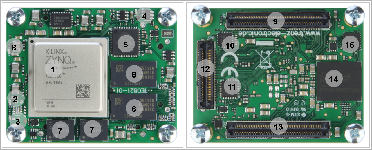
The Trenz Electronic TE0821 -01-3BI21FA is a powerful 4 x 5 cm MPSoC module integrated with a Xilinx Zynq UltraScale+ ZU3EGMPSoC. In addition, the module is equipped with a 2 2x 1 GB DDR4 SDRAM chip, 4Gb up to 128 Gb eMMC chip, 2x 64 MB flash memory for configuration and data storage, as well as powerful switching power supplies for all required voltages. . The module is equipped with a Lattice Mach XO2 CPLD for system controlling. 3x Robust high-speed connectors provide a large number of inputs and outputs.
This module is pin compatible with Trenz Electronic TE0820 MPSoC modules (JM2 pin 100 is not connected).
The highly integrated modules are smaller than a credit card and are offered in several variants at an affordable price-performance ratio. Modules with a 4 x 5 cm form factor are completely mechanically and largely electrically compatible with each other.
All components cover at least the industrial temperature range from -40 ° C to + 85 ° C. The temperature range in which the module can be used depends on the customer design and the selected cooling. Please contact us for special solutions.
...
| Page properties |
|---|
|
Note:
'description: Important components and connector or other Features of the module
→ please sort and indicate assembly options Key Features' must be split into 6 main groups for modules and mainboards: - SoC/FPGA
- Package: SFVC784
- Device: ZU2...ZU5*
- Engine: CG, EG, EV*
- Speed: -1LI, -2LE,*, **
- Temperature: I, E,*, **
- RAM/Storage
- Low Power DDR4 on PS
- Data width: 32bit
- Size: def. 2GB*
- Speed:***
- eMMC
- Data width: 8Bit
- size: def. 8GB *
- QSPI boot Flash in dual parallel mode (size depends on assembly version)
- Data width: 8bit
- size: def. 128MB *
- HyperRAM/Flash (optional, default not assembled)
- MAC address serial EEPROM with EUI-48™ node identity (Microchip 24AA025E48)
- On Board
- Lattice LCMXO2
- PLL SI5338
- Gigabit Ethernet transceiver PHY (Marvell Alaska 88E1512)
- Hi-speed USB2 ULPI transceiver with full OTG support (Microchip USB3320C)
- Interface
- 132 x HP PL I/Os (3 banks)
- ETH
- USB
- 4 GTR (for USB3, Sata, PCIe, DP)
- MIO for UART
- MIO for SD
- MIO for PJTAG
- JTAG
- Ctrl
- Power
- 3.3V-5V Main Input
- 3.3V Controller Input
- Variable Bank IO Power Input
- Dimension
- Notes
- * depends on assembly version
- ** also non low power assembly options possible
- *** depends on used U+ Zynq and DDR4 combination
Key Features' must be split into 6 main groups for carrier: - Modules
- TE0808, TE807, TE0803,...
- RAM/Storage
- On Board
- Interface
- E.g. ETH, USB, B2B, Display port
- Power
- E.g. Input supply voltage
- Dimension
|
- SoC/FPGA
- Package: SFVC784
- Device: ZU2 ...ZU5, *
- Engine: EG, CG, EV, *
- Speed: -1, -1L, -2, -2L, 3, *, **
- Temperature: I, E, *, **Xilinx Zynq UltraScale+ XCZU3EG-1SFVC784I
- ZU3EG, 784 Pin Packages
- Application Processor: Quad-Core ARM Cortex-A53 MPCore
- Real-Time Processor: Dual-core ARM Cortex-R5 MPCore
Graphics Processor: Mali-400 MP2
RAM/Storage- 2 GByte 2x DDR4 SDRAM, 32-Bit databus-width
- Data Width: 16 Bit
- Size: 8 Gb, *
- Speed: 2400 Mbps, ***
- 2x 128 MByte QSPI boot Flash in dual parallel mode
- Data Width: 8 Bit
- Size: 512 Mb Gb, *
- 1x e.MMC Memory
- Data Width: 16 Bit
- Size: 8 Gb, *
8 GByte e.MMC Memory (up to 64 GByte) - MAC address serial EEPROM with EUI-48 node identity
On Board
- Graphic Processing Unit (GPU) :Mali-400 MP2
- Lattice MachXO2 CPLD
- Programmable Clock Generator
- Hi-speed USB2 ULPI Transceiver
- 4x LEDS
Interface- 1 Gbps RGMII Ethernet interface
- Hi-speed USB2 ULPI transceiver with full OTG support
- Graphic Processor Mali-400 MP2, *
- 156 x High Performance (HP) und 96 x High Density PL I/Os
- 4 x serial PS GTR transceivers
Interface- PCI Express interface version 2.1 compliant
- SATA 3.1 specification compliant interface
- DisplayPort source-only interface with video
resolution up to 4k x 2k
- 2x USB 3.0 specification compliant interface implementing a 5 Gbit/s line rate
- 1 GB/s serial GMII interface
- Hi-speed USB2 ULPI transceiver with full OTG support
- 34 x High Performance und 96 x High Density PL I/Os
- 14 x PS MIOs (6 of the MIOs intended for SD card interface in default configuration)
Power- All power regulators on board
DimensionNote- * depends on assembly version
- ** also non low power assembly options possible
- *** depends on used U+ Zynq and DDR4 combination4 x serial PS GTR transceivers
- Rugged for shock and high vibration
Power- All power supplies on board
DimensionBlock Diagram
| Page properties |
|---|
|
add drawIO object here.
|
...
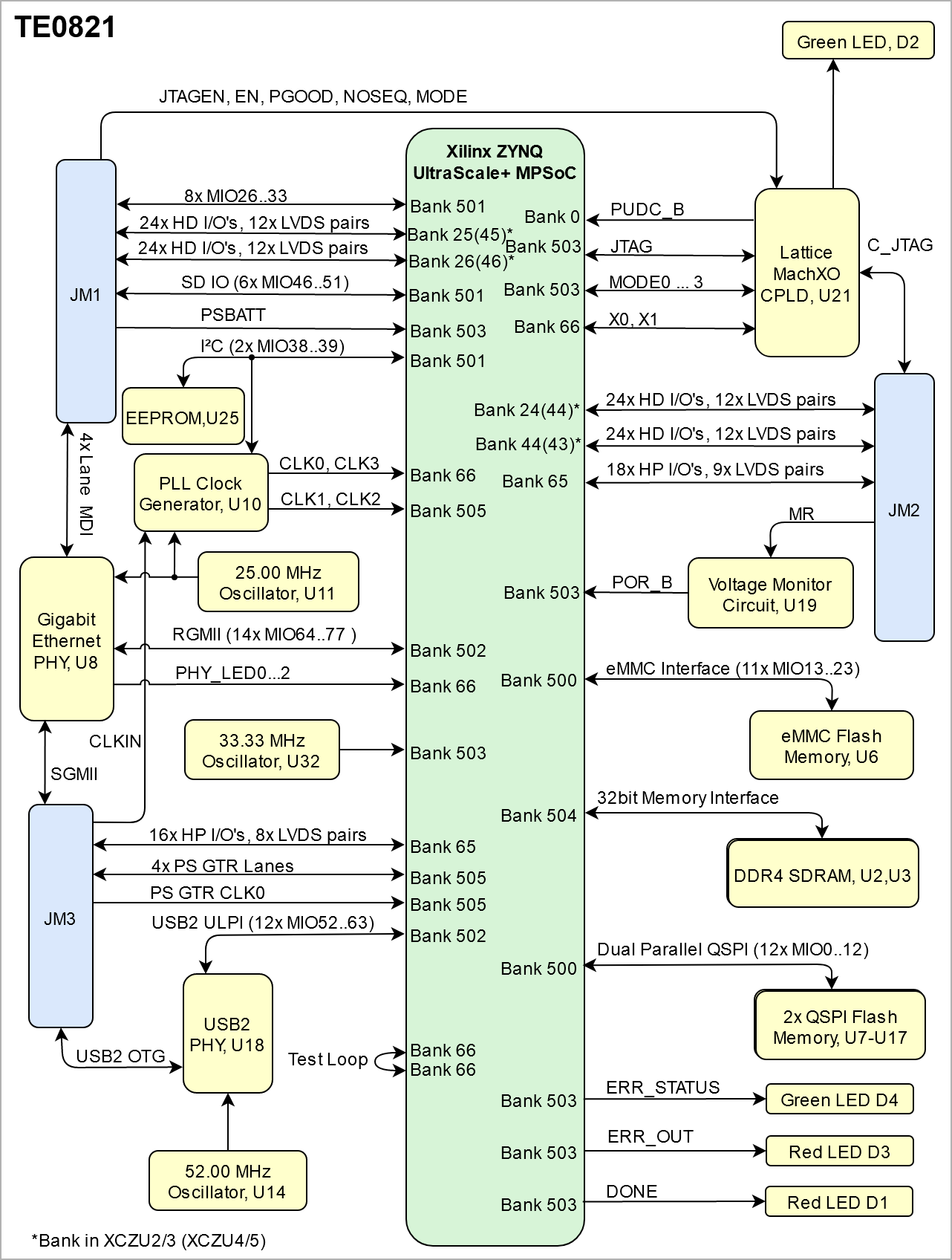
| Scroll Title |
|---|
| anchor | Figure_OV_BD |
|---|
| title | TE0821 block diagram |
|---|
|
| Scroll Ignore |
|---|
| draw.io Diagram |
|---|
| border | false |
|---|
| |
|---|
| diagramName | TE0821_OV_BD |
|---|
| simpleViewer | false |
|---|
| width | |
|---|
| links | auto |
|---|
| tbstyle | hidden |
|---|
| diagramDisplayName | |
|---|
| lbox | true |
|---|
| diagramWidth | 641 |
|---|
| revision | 819 |
|---|
|
|
| Scroll Only |
|---|
|
|
Main Components
...
| Scroll Title |
|---|
| anchor | Figure_OV_MC |
|---|
| title | TE0821 main components |
|---|
|
| Scroll Ignore |
|---|
| draw.io Diagram |
|---|
| border | false |
|---|
| |
|---|
| diagramName | TE0821_OV_MC |
|---|
| simpleViewer | false |
|---|
| width | |
|---|
| links | auto |
|---|
| tbstyle | hidden |
|---|
| diagramDisplayName | |
|---|
| lbox | true |
|---|
| diagramWidth | 641 |
|---|
| revision | 79 |
|---|
|
|
| Scroll Only |
|---|
|
|
- Xilinx Zynq ZYNQ UltraScale+ XCZU3EGMPSoC, U1
- Red LED (ERR_OUT), D3
- Green LED (ERR_STATUS), D4
- Red LED (DONE), D1
- 10/100/1000 Mbps energy efficient ethernet transceiverEnergy Efficient Ethernet Transceiver, U8
- 8Gb DDR4, U2-U3
- 512 Mbit QSPI flash memory, U7-U17
- Green User LED, D2
- B2B connector Samtec Razor Beam, JM1
- Green User LED, D2
- Programmable clock generator, U10
- USB2.0 Transceiver, U18
- B2B connector Samtec Razor Beam, JM3
- B2B connector Samtec Razor Beam, JM2
- 8 GByte eMMC memory, U6
- Lattice Semiconductor MachXO2 System Controller CPLD, U21
Additional assembly options are available for cost or performance optimization upon request.
Initial Delivery Initial Delivery State
| Page properties |
|---|
|
Notes : Only components like EEPROM, QSPI flash can be initialized by default at manufacture. If there is no components which might have initial data ( possible on carrier) you must keep the table empty |
...
| Scroll Title |
|---|
| anchor | Table_OV_IDS |
|---|
| title | Initial delivery state of programmable devices on the module |
|---|
|
| Scroll Table Layout |
|---|
| orientation | portrait |
|---|
| sortDirection | ASC |
|---|
| repeatTableHeaders | default |
|---|
| style | |
|---|
| widths | |
|---|
| sortByColumn | 1 |
|---|
| sortEnabled | false |
|---|
| cellHighlighting | true |
|---|
|
Storage device name | Content | Notes |
|---|
Dual QSPI Flash Memory | Not programmed |
| eMMC Memory | Not programmed |
| | DDR4 SDRAM | Not programmed |
| | Programmable Clock Generator | Not programmed |
| | CPLD (LCMXO2-256HC)SC0820-02 QSPI Firmware | Programmed | TE0821 CPLD |
|
Configuration Signals
| Page properties |
|---|
|
- Overview of Boot Mode, Reset, Enables.
|
...
| Scroll Title |
|---|
| anchor | Table_OV_BP |
|---|
| title | Boot process. |
|---|
|
| Scroll Table Layout |
|---|
| orientation | portrait |
|---|
| sortDirection | ASC |
|---|
| repeatTableHeaders | default |
|---|
| style | |
|---|
| widths | |
|---|
| sortByColumn | 1 |
|---|
| sortEnabled | false |
|---|
| cellHighlighting | true |
|---|
|
MODE Pin | Boot Mode |
|---|
| LowHigh | QSPI* | | HighLow | SD Card* |
|
*changable also with other CPLD Firmware: TE0821 CPLD.
| Scroll Title |
|---|
| anchor | Table_OV_RST |
|---|
| title | Reset process. |
|---|
|
| Scroll Table Layout |
|---|
| orientation | portrait |
|---|
| sortDirection | ASC |
|---|
| repeatTableHeaders | default |
|---|
| style | |
|---|
| widths | |
|---|
| sortByColumn | 1 |
|---|
| sortEnabled | false |
|---|
| cellHighlighting | true |
|---|
|
Signal | B2B | I/O | Note |
|---|
EN | JM1-28 | Input | CPLD Enable Pin |
|
...
| Scroll Title |
|---|
| anchor | Table_SIP_B2B |
|---|
| title | General PL I/O to B2B connectors information |
|---|
|
| Scroll Table Layout |
|---|
| orientation | portrait |
|---|
| sortDirection | ASC |
|---|
| repeatTableHeaders | default |
|---|
| style | |
|---|
| widths | |
|---|
| sortByColumn | 1 |
|---|
| sortEnabled | false |
|---|
| cellHighlighting | true |
|---|
|
| FPGA Bank | Type | B2B Connector | I/O Signal Count | Voltage Level | Notes |
|---|
| 24 | HD | JM2 | 24x I/O, 12x LVDS Pairs | Variable | Max voltage 3.3V | | 25 | HD | JM1 | 24x I/O, 12x LVDS Pairs | Variable | Max voltage 3.3V | | 26 | HD | JM1 | 24x I/O, 12x LVDS Pairs | Variable | Max voltage 3.3V | | 44 | HD | JM2 | 24x I/O, 12x LVDS Pairs | Variable | Max voltage 3.3V | | 65 | HP | JM2 | 18x I/O, 9x LVDS Pairs | Variable | Max voltage 1.8V | 65 | HP | JM3 | 16x I/O, 8x LVDS Pairs | Variable | Max voltage 1.8V | | 505 | GTR | JM3 | 16x I/O, 8x LVDS Pairs | - | 4x lanes | | 505 | GTR CLK | JM3 | 1x Diff Clock | - |
| 501 | MIO | JM1 | 15 I/O | 3.3V |
|
|
For detailed information about the pin-out, please refer to the Pin-out table.
JTAG Interface
JTAG access to the Xilinx Zynq UltraScale+ is applicable by using Lattice MachXO CPLD through B2B connector JM2.
...
There are 4x MGT Lanes connected to FPGA Bank 505-GTR. The Xilinx Zynq UltraScale+ device used on the TE0821 module has 4 GTR transceivers. All 4 are wired directly to B2B connector JM3. MGT (Multi Gigabit Transceiver) lane consists of one transmit and one receive (TX/RX) differential pairs, four signals total per one MGT lane. Following table lists lane number, FPGA bank number, transceiver type, signal schematic name, board-to-board pin connection and FPGA pins connection:
| Scroll Title |
|---|
|
| Scroll Title |
|---|
| anchor | Table_SIP_MGT |
|---|
| title | MGT Lanes connection |
|---|
|
| Scroll Table Layout |
|---|
| orientation | portrait |
|---|
| sortDirection | ASC |
|---|
| repeatTableHeaders | default |
|---|
| style | |
|---|
| widths | |
|---|
| sortByColumn | 1 |
|---|
| sortEnabled | false |
|---|
| cellHighlighting | true |
|---|
|
Lane | Schematic | B2B | Note |
|---|
| 0 | - B505_RX0_P
- B505_RX0_N
- B505_TX0_P
- B505_TX0_N
| |
| | 1 | - B505_RX1_P
- B505_RX1_N
- B505_TX1_P
- B505_TX1_N
| |
| | 2 | - B505_RX2_P
- B505_RX2_N
- B505_TX2_P
- B505_TX2_N
| |
| | 3 | - B505_RX2_P
- B505_RX2_N
- B505_TX2_P
- B505_TX2_N
| |
|
|
Gigabit Ethernet
On-board Gigabit Ethernet PHY is provided with Marvell Alaska 88E1512 chip. The Ethernet PHY RGMII interface is connected to the Zynq Ethernet0 PS GEM0. I/O voltage is fixed at 1.8V for HSTL signaling. SGMII (SFP copper or fiber) can be used directly with the Ethernet PHY, as the SGMII pins are available on the B2B connector JM3. The reference clock input of the PHY is supplied from an on-board 25MHz oscillator (U11), the 125MHz output clock is left unconnected.
| Scroll Title |
|---|
| anchor | Table_SIP_ETH |
|---|
| title | GigaBit Ethernet connection |
|---|
|
| Scroll Table Layout |
|---|
| orientation | portrait |
|---|
| sortDirection | ASC |
|---|
| repeatTableHeaders | default |
|---|
| style | |
|---|
| widths | |
|---|
| sortByColumn | 1 |
|---|
| sortEnabled | false |
|---|
| cellHighlighting | true |
|---|
|
| Pin | Schematic | Connected to | Note |
|---|
| MDIP0...3 | PHY_MDI0...3 | B2B, JM1 |
| | MDC | ETH_MDC | MIO76 |
| | MDIO | ETH_MDIO | MIO77 |
| | S_IN | S_IN | B2B, JM3 |
| | S_OUT | S_OUT | B2B, JM3 |
| | TXD0..3 | ETH_TXD0...3 | MIO65...68 |
| | TX_CTRL | ETH_TXCTL | MIO69 |
| | TX_CLK | ETH_TXCK | MIO64 |
| | RXD0...3 | ETH_RXD0...3 | MIO71...74 |
| | RX_CTRL | ETH_RXCTL | MIO75 |
| | RX_CLK | ETH_RXCK | MIO70 |
| | LED0...2 | PHY_LED0...2 | FPGA Bank 66 |
| | RESETn | ETH_RST | MIO24 |
|
|
...
| Scroll Title |
|---|
| anchor | Table_SIP_CPLD |
|---|
| title | System Controller CPLD special purpose pins |
|---|
|
| Scroll Table Layout |
|---|
| orientation | portrait |
|---|
| sortDirection | ASC |
|---|
| repeatTableHeaders | default |
|---|
| style | |
|---|
| widths | |
|---|
| sortByColumn | 1 |
|---|
| sortEnabled | false |
|---|
| cellHighlighting | true |
|---|
|
| Pin Name | Mode | Function | Default Configuration |
|---|
| EN1 | Input | Power Enable | No hard wired function on PCB. When forced low, PGOOD goes low without effect on power management | | PGOOD | Output | Power Good | Only indirect used for power status, see CPLD description | | NOSEQ | - | - | No used for Power sequencing, see CPLD description | | RESIN | Input | Reset | Active low reset, gated to POR_B | | JTAGEN | Input | JTAG Select | Low for normal operation, high for CPLD JTAG access |
|
Please check the entire information at TE0821 CPLD.
USB Interface
USB PHY is provided by Microchip USB3320. The ULPI interface is connected to the Zynq PS USB0. I/O voltage is fixed at 1.8V. Reference clock input for the USB PHY is supplied by the on-board 52.00 MHz oscillator (U14).
| Scroll Title |
|---|
| anchor | Table_SIP_USB |
|---|
| title | General overview of the USB PHY signals |
|---|
|
| Scroll Table Layout |
|---|
| orientation | portrait |
|---|
| sortDirection | ASC |
|---|
| repeatTableHeaders | default |
|---|
| style | |
|---|
| widths | |
|---|
| sortByColumn | 1 |
|---|
| sortEnabled | false |
|---|
| cellHighlighting | true |
|---|
|
| PHY Pin | ZYNQ Pin | B2B Name | Notes |
|---|
| ULPI | MIO52..63 | - | Zynq USB0 MIO pins are connected to the USB PHY. | | REFCLK | - | - | 52. |
000000 | 00 MHz from on-board oscillator (U14). | | REFSEL[0..2] | - | - | Reference clock frequency select, all set to GND selects 52. |
000000 | 00 MHz. | | RESETB | MIO25 | - | Active low reset. | | CLKOUT | MIO52 | - | Connected to 1.8V, selects reference clock operation mode. | | DP, DM | - | OTG_D_P, OTG_D_N | USB data lines routed to B2B connector JM3 pins 47 and 49. | | CPEN | - | VBUS_V_EN | External USB power switch active high enable signal, routed to JM3 pin 17. | | VBUS | - | USB_VBUS | Connect to USB VBUS via a series of resistors, see reference schematics, routed to JM3 pin 55. | | ID | - | OTG_ID | For an A-device connect to ground, for a B-device left floating. routed from JM3 pin 23. |
|
MIO Pins
I2C Interface
On-board I2C devices are connected to MIO38 (SCL) and MIO39 (SDA) which are configured as I2C0 by default. Addresses for on-board I2C slave devices are listed in the table below:
| Scroll Title |
|---|
| anchor | Table_SIP_I2C |
|---|
| title | Address table of the I2C bus slave devices |
|---|
|
| Scroll Table Layout |
|---|
| orientation | portrait |
|---|
| sortDirection | ASC |
|---|
| repeatTableHeaders | default |
|---|
| style | |
|---|
| widths | |
|---|
| sortByColumn | 1 |
|---|
| sortEnabled | false |
|---|
| cellHighlighting | true |
|---|
|
| I2C Device | I2C Address | Notes |
|---|
Si5338A PLL | 0x70 | - | | EEPROM | 0x50 | - |
|
MIO Pins
| Page properties |
|---|
|
you must fill the table below with group of MIOs which are connected to a specific components or peripherals, you |
| Page properties |
|---|
|
you must fill the table below with group of MIOs which are connected to a specific components or peripherals, you do not have to specify pins in B2B, Just mention which B2B is connected to MIOs. The rest is clear in the Schematic. Example: | MIO Pin | Connected to | B2B | Notes |
|---|
| MIO12...14 | SPI_CS , SPI_DQ0... SPI_DQ3, SPI_SCK | J2 | QSPI |
|
...
| Scroll Title |
|---|
| anchor | Table_SIP_TPs |
|---|
| title | Test Points Information |
|---|
|
| Scroll Table Layout |
|---|
| orientation | portrait |
|---|
| sortDirection | ASC |
|---|
| repeatTableHeaders | default |
|---|
| style | |
|---|
| widths | |
|---|
| sortByColumn | 1 |
|---|
| sortEnabled | false |
|---|
| cellHighlighting | true |
|---|
|
| Test Point | Signal | Connected to | Notes |
|---|
| 1 | I2C_SCL | EEPROM, U25 |
| | 2 | I2C_SDA | EEPROM, U25 |
| | 3 | SRST_B | FPGA Bank 503 | PSCONFIG | | 4 | PS_CLK | FPGA Bank 503 | PSCONFIG | | 5 | PROG_B | FPGA Bank 503 | PSCONFIG | | 6 | INIT_B | FPGA Bank 503 | PSCONFIG | | 7 | DONE | Red LED, D1 |
| | 8 | PS_LP0V85 | Voltage Regulator, U12 |
| | 9 | DDR_2V5 | Voltage Regulator, U4 |
| | 10 | PS_AVCC | Voltage Regulator, U9 |
| | 11 | DDR_1V2 | Voltage Regulator, U15 |
| | 12 | PS_AVTT | Voltage Regulator, U3U13 |
| | 13 | PS_FP0V85 | Voltage Regulator, U26 |
| | 14 | POR_B | Voltage Translator, U19 |
| | 15 | PS_PLL | Voltage Regulator, U23 |
| | 16 | PL_VCCINT | Voltage Regulator, U5 |
|
|
...
| Scroll Title |
|---|
| anchor | Table_OBP |
|---|
| title | On board peripherals |
|---|
|
| Scroll Table Layout |
|---|
| orientation | portrait |
|---|
| sortDirection | ASC |
|---|
| repeatTableHeaders | default |
|---|
| style | |
|---|
| widths | |
|---|
| sortByColumn | 1 |
|---|
| sortEnabled | false |
|---|
| cellHighlighting | true |
|---|
|
|
Quad SPI Flash Memory
...
The TE0821 is equipped with dual Flash Memory, U7, U17. Two quad SPI compatible serial bus flash MT25QU512ABB8E12-0SIT memory chips are provided for FPGA configuration file storage. After configuration completes the remaining free memory can be used for application data storage. All four SPI data lines are connected to the FPGA allowing x1, x2 or x4 data bus widths to be used. The maximum data transfer rate depends on the bus width and clock frequency.
| Scroll Title |
|---|
| anchor | Table_OBP_SPI |
|---|
| title | Quad SPI interface MIOs and pins |
|---|
|
| Scroll Table Layout |
|---|
| orientation | portrait |
|---|
| sortDirection | ASC |
|---|
| repeatTableHeaders | default |
|---|
| style | |
|---|
| widths | |
|---|
| sortByColumn | 1 |
|---|
| sortEnabled | false |
|---|
| cellHighlighting | true |
|---|
|
| Pin | Schematic | Notes |
|---|
| U7 Pin | U17 Pin |
|---|
| nCS | MIO5 | MIO7 |
| | CLK | MIO0 | MIO12 |
| | DI/IO0 | MIO4 | MIO8 |
| | DO/IO1 | MIO1 | MIO9 |
| | nHOLD/IO3 | MIO3 | MIO11 |
| | WP/IO2 | MIO2 | MIO10 |
|
|
...
- Part number: K4A8G165WB-BIRC
- Supply voltage: 1.2V
- Speed: 2400 Mbps
- Temperature: -40 ~ 95 °C
GigaBit Ethernet
System Controller CPLD
The System Controller CPLD (U21) is provided by Lattice Semiconductor LCMXO2-256HC (MachXO2 product family). It is the central system management unit with module specific firmware installed to monitor and control various signals of the FPGA, on-board peripherals, I/O interfaces and module as a whole.
See also TE0821 System Controller CPLD page.
GigaBit Ethernet
On-board Gigabit Ethernet PHY (U8) is provided with Marvell Alaska 88E1512 IC (U8). The Ethernet PHY RGMII interface is connected to the ZynqMP Ethernet3 PS GEM3. I/O voltage is fixed at 1.8V for HSTL signaling. The reference clock input of the PHY is supplied from an on-board 25.00 MHz oscillator (U11).
| Scroll Title |
|---|
| anchor | Table_OBP_ETH |
|---|
| title | Ethernet PHY to Zynq SoC connections |
|---|
|
|
| Scroll Title |
|---|
| anchor | Table_OBP_ETH |
|---|
| title | Ethernet PHY to Zynq SoC connections |
|---|
|
| scroll-tablelayout |
|---|
| orientation | portrait |
|---|
| sortDirection | ASC |
|---|
| repeatTableHeaders | default |
|---|
| style | |
|---|
| widths | |
|---|
| sortByColumn | 1 |
|---|
| sortEnabled | false |
|---|
| cellHighlighting | true |
|---|
|
| Pin | Schematic | Connected to | Note |
|---|
| MDIP0...3 | PHY_MDI0...3 | B2B, JM1 |
| | MDC | ETH_MDC | MIO76 |
| | MDIO | ETH_MDIO | MIO77 |
| | S_IN | S_IN | B2B, JM3 |
| | S_OUT | S_OUT | B2B, JM3 |
| | TXD0..3 | ETH_TXD0...3 | MIO65...68 |
| | TX_CTRL | ETH_TXCTL | MIO69 |
| | TX_CLK | ETH_TXCK | MIO64 |
| | RXD0...3 | ETH_RXD0...3 | MIO71...74 |
| | RX_CTRL | ETH_RXCTL | MIO75 |
| | RX_CLK | ETH_RXCK | MIO70 |
| | LED0...2 | PHY_LED0...2 | FPGA Bank 66 |
| | RESETn | ETH_RST | MIO24 |
|
Clock Sources
...
| anchor | Table_OBP_CLK |
|---|
| title | Osillators |
|---|
...
USB2.0 Transceiver
Hi-speed USB ULPI PHY (U18) is provided with USB3320 from Microchip. The ULPI interface is connected to the Zynq PS USB0 via MIO52..63, bank 502. The I/O voltage is fixed at 1.8V and PHY reference clock input is supplied from the on-board 52.00 MHz oscillator (U14).
eMMC Flash Memory
eMMC Flash memory device(U6) is connected to the ZynqMP PS MIO bank 500 pins MIO13..MIO23. eMMC chips IS21ES08G-JCLI (FLASH - NAND Speicher-IC (64 Gb x 1) MMC ) is used.
Clock Sources
| Scroll Title |
|---|
| anchor | Table_OBP_CLK |
|---|
| title | Osillators |
|---|
|
| Scroll Table Layout |
|---|
| orientation | portrait |
|---|
| sortDirection | ASC |
|---|
| repeatTableHeaders | default |
|---|
| style | |
|---|
| widths | |
|---|
| sortByColumn | 1 |
|---|
| sortEnabled | false |
|---|
| cellHighlighting | true |
|---|
|
| Designator | Description | Frequency | Note |
|---|
| U11 | MEMS Oscillator | 25 MHz |
| | U14 | MEMS Oscillator | 52 MHz |
| | U32 | MEMS Oscillator | 80 MHz |
|
|
Programmable Clock Generator
There is a Silicon Labs I2C programmable clock generator Si5338A (U10) chip on the module. It's output frequencies can be programmed using the I2C bus address 0x70 or 0x71. Default address is 0x70, IN4/I2C_LSB pin must be set to high for address 0x71.
A 25.00 MHz oscillator is connected to the pin IN3 and is used to generate the output clocks. The oscillator has its output enable pin permanently connected to 1.8V power rail, thus making output frequency available as soon as 1.8V is present. Three of the Si5338 clock outputs are connected to the FPGA. One is connected to a logic bank and the other two are connected to the GTR banks.
Once running, the frequency and other parameters can be changed by programming the device using the I2C bus connected between the FPGA (master) and clock generator (slave). For this, proper I2C bus logic has to be implemented in FPGA
...
Programmable Clock Generator
There is a programmable clock generator on-board (U10) provided in order to generate variable clocks for the module. Programming can be done using I2C via PIN header J??. The I2C Address is 0x70 or 0x71.
| Scroll Title |
|---|
| anchor | Table_OBP_PCLK |
|---|
| title | Programmable Clock Generator Inputs and Outputs |
|---|
|
| Scroll Table Layout |
|---|
| orientation | portrait |
|---|
| sortDirection | ASC |
|---|
| repeatTableHeaders | default |
|---|
| sortByColumn | 1 |
|---|
| sortEnabled | false |
|---|
| cellHighlighting | true |
|---|
|
| U25 Pin | Signal | Connected to | Direction | Note |
|---|
IN0..1 | CLK_IN | JM3 | IN |
| | IN2 | CLK_25M | Oscillator, U11 | IN |
| | SCL | I2C_SCL | EEPROM,U25 | INOUT |
| | SDA | I2C_SDA | EEPROM,U25 | INOUT |
| | CLK0 | CLK0 | JM3 | OUT |
| | CLK1 | B505_CLK3 | FPGA Bank 505 | IN |
| | CLK2 | B505_CLK1 | FPGA Bank 505 | IN |
| | CLK3 | CLK3_N |
| IN |
|
|
...
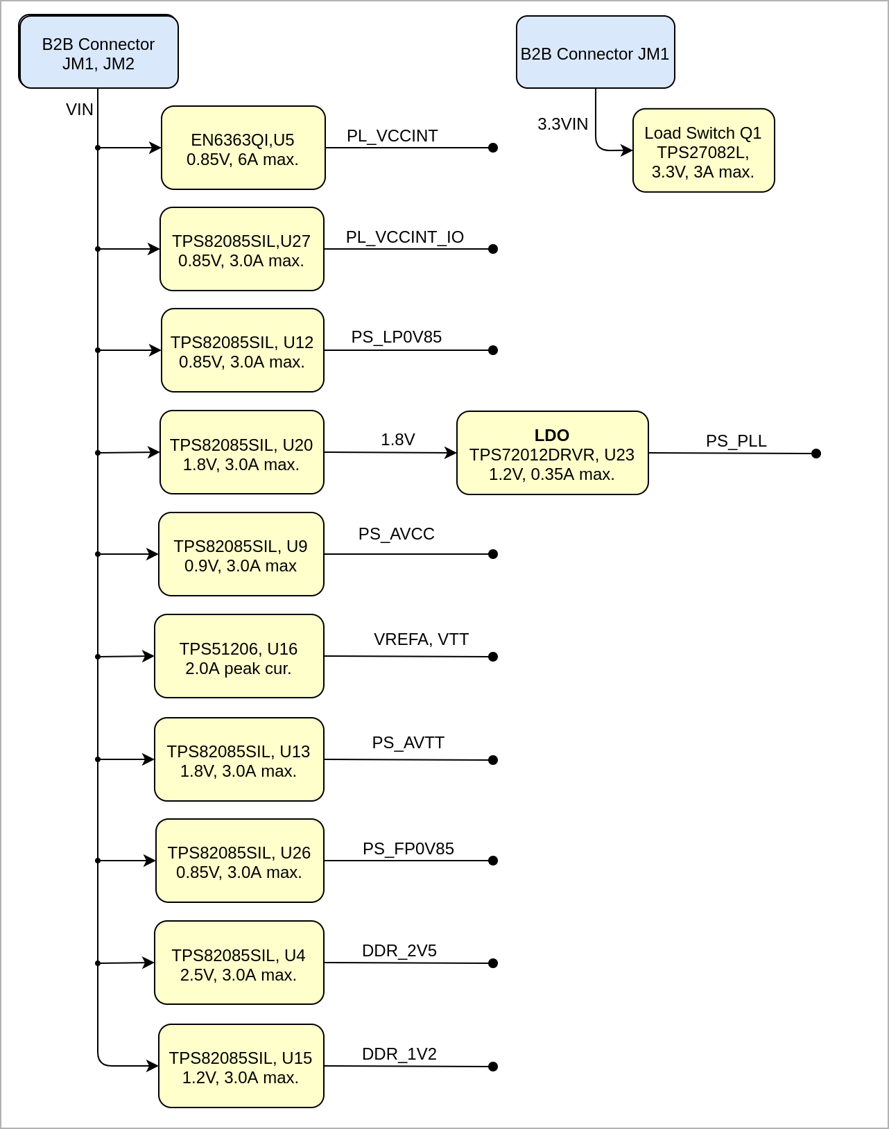
Power supply with minimum current capability of xx 3 A for system startup is recommended.
...
| Scroll Title |
|---|
| anchor | Figure_PWR_PD |
|---|
| title | Power Distribution |
|---|
|
| Scroll Ignore |
|---|
| scroll-pdf | true |
|---|
| scroll-office | true |
|---|
| scroll-chm | true |
|---|
| scroll-docbook | true |
|---|
| scroll-eclipsehelp | true |
|---|
| scroll-epub | true |
|---|
| scroll-html | true |
|---|
| | draw.io Diagram |
|---|
| border | false |
|---|
| |
|---|
| diagramName | TE0821_PWR_PD |
|---|
| simpleViewer | false |
|---|
| width | |
|---|
| links | auto |
|---|
| tbstyle | hidden |
|---|
| diagramDisplayName | |
|---|
| lbox | true |
|---|
| diagramWidth | 641 |
|---|
| revision | 5 |
|---|
|
|
| Scroll Only |
|---|
|
|
...
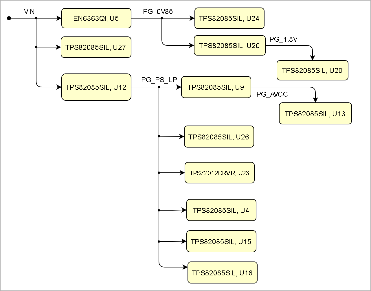
| Scroll Title |
|---|
| anchor | Figure_PWR_PS |
|---|
| title | Power Sequency |
|---|
|
| Scroll Ignore |
|---|
| draw.io Diagram |
|---|
| border | false |
|---|
| |
|---|
| diagramName | TE0821_PWR_PS |
|---|
| simpleViewer | false |
|---|
| width | |
|---|
| links | auto |
|---|
| tbstyle | hidden |
|---|
| diagramDisplayName | |
|---|
| lbox | true |
|---|
| diagramWidth | 641 |
|---|
| revision | 68 |
|---|
|
|
| Scroll Only |
|---|
|
|
Power Rails
| Scroll Title |
|---|
| anchor | Table_PWR_PR |
|---|
| title | Module power rails. |
|---|
|
| Scroll Table Layout |
|---|
| orientation | portrait |
|---|
| sortDirection | ASC |
|---|
| repeatTableHeaders | default |
|---|
| style | |
|---|
| widths | |
|---|
| sortByColumn | 1 |
|---|
| sortEnabled | false |
|---|
| cellHighlighting | true |
|---|
|
| Power Rail Name | B2B JM1 Pin | B2B JM2 Pin | B2B JM3 Pin | Direction | Notes |
|---|
| VIN | 1, 3, 5 | 2, 4, 6, 8 | - | Input | Supply voltage from the carrier board | | 3.3V | - | 10, 12 | - | Output | Internal 3.3V voltage level | | VCCO_HD25_26 | 9,11 |
| - | Input | 0 to 3.3V Voltage | | 3.3VIN | 13, 15 | - | - | Input | Supply voltage from the carrier board | | 1.8V | 39 | - | - | Output | Internal 1.8V voltage level | | JTAG VREF | - | 91 | - | Output | JTAG reference voltage.
Attention: Net name on schematic is "3.3VIN" | | VCCO_HD24_ |
64High performance I/O bank voltage| 0 to 3.3V Voltage | | VCCO_65 | - | 5 | - | Input |
High performance I/O bank voltage | | 0 to 1.8V Voltage | | PSBATT | 79 | - |
VCCO_66 | 9, 11High performance I/O bank voltage
|
Bank Voltages
| Scroll Title |
|---|
| anchor | Table_PWR_BV |
|---|
| title | Zynq SoC bank voltages. |
|---|
|
| Scroll Table Layout |
|---|
| orientation | portrait |
|---|
| sortDirection | ASC |
|---|
| repeatTableHeaders | default |
|---|
style | widths | | sortByColumn | 1 |
|---|
| sortEnabled | false |
|---|
| cellHighlighting | true |
|---|
| | sortDirection | ASC |
|---|
| repeatTableHeaders | default |
|---|
| style | |
|---|
| widths | |
|---|
| sortByColumn | 1 |
|---|
| sortEnabled | false |
|---|
| cellHighlighting | true |
|---|
|
| FPGA Bank | Schematic | Voltage | Note |
|---|
| Bank 24 HD | VCCO_HD24_44 | Variable | Max voltage 3.3V | | Bank 25 HD | VCCO_HD25_26 | Variable | Max voltage 3.3V | | Bank 26 HD | VCCO_HD25_26 | Variable | Max voltage 3.3V | | Bank 44 HD | VCCO_HD24_44 | Variable | Max voltage 3.3V | | Bank |
| Schematic Name | | Notes |
|---|
User | HP: 1.0V to 1.8V | | N.C | Not Connected | | Bank 65 HP | VCCO_65 |
User | HP: 1.0V to UserHP: 1.0V to | 1.8V |
| | Bank 500 PSMIO | VCCO_PSIO0_500 | 1.8V |
- |
| Bank 501 PSMIO | VCCO_PSIO1_501 | 3.3V |
- |
| | Bank 502 PSMIO | VCCO_PSIO2_502 | 1.8V |
- |
| | Bank 503 PSCONFIG | VCCO_PSIO3_503 | 1.8V |
- | VCCOPSDDR_504-
|
Board to Board Connectors
| Page properties |
|---|
|
- This section is optional and only for modules.
use "include page" macro and link to the general B2B connector page of the module series, For example: 6 x 6 SoM LSHM B2B Connectors
| Include Page |
|---|
| PD:6 x 6 SoM LSHM B2B ConnectorsPD: |
|---|
| 6 x 6 SoM LSHM B2B Connectors |
|---|
|
|
| Include Page |
|---|
| PD:4 x 5 SoM LSHM B2B ConnectorsPD: |
|---|
| 4 x 5 SoM LSHM B2B Connectors |
|---|
|
...
| Scroll Title |
|---|
| anchor | Table_TS_AMR |
|---|
| title | PS absolute maximum ratings |
|---|
|
| Scroll Table Layout |
|---|
| orientation | portrait |
|---|
| sortDirection | ASC |
|---|
| repeatTableHeaders | default |
|---|
| style | |
|---|
| widths | |
|---|
| sortByColumn | 1 |
|---|
| sortEnabled | false |
|---|
| cellHighlighting | true |
|---|
|
| Description | Min | Max | Unit | Notes |
|---|
VIN supply voltage | -0.3 | 7 | V | See EN6347QI and TPS82085SIL datasheets | | 3.3VIN supply 3VIN supply voltage | -0.1 | 3.630 | V | Xilinx DS925 and TPS27082L datasheet | | PS I/O supply voltage, VCCO_PSIO | -0.5 | 3.630 | V | Xilinx document DS925 | | PS I/O input voltage | -0. | 13.6305 | VCCO_PSIO + 0.55 | V | Xilinx document DS925 | | HP | DS925 and TPS27082L datasheetPS I/O bank supply voltage, VCCO | _PSIO | -0.5 | 32. | 6300 | V | Xilinx document DS925 | PS | HP I/O bank input voltage | -0. | 555 | VCCO | _PSIO + 0.55 | V | Xilinx document DS925HP | | HD I/O bank supply voltage, VCCO | -0.5 | 23. | 04 | V | Xilinx document DS925 | HP | HD I/O bank input voltage | -0.55 | VCCO + 0.55 | V | Xilinx document DS925 | | PS GTR reference clocks absolute input voltage | -0.5 | 1.1 | V | Xilinx document DS925 | | PS GTR absolute input voltage | -0.5 | 1.1 | V | Xilinx document DS925 | Voltage on SC CPLD pins | -0.5 | 3.75 | V | Lattice Semiconductor MachXO2 datasheet | Storage temperature | -40 | +85 | °C | See eMMC datasheet |
|
Recommended Operating Conditions
...
| Scroll Title |
|---|
| anchor | Table_TS_ROC |
|---|
| title | Recommended operating conditions. |
|---|
|
| Scroll Table Layout |
|---|
| orientation | portrait |
|---|
| sortDirection | ASC |
|---|
| repeatTableHeaders | default |
|---|
| style | |
|---|
| widths | |
|---|
| sortByColumn | 1 |
|---|
| sortEnabled | false |
|---|
| cellHighlighting | true |
|---|
|
| Parameter | Min | Max | Units | Reference Document |
|---|
| VIN supply voltage | 3.3 | 6 | V | See TPS82085S datasheet | | 3.3VIN supply voltage | 3.3 | 3.465 | V | See LCMXO2-256HC, Xilinx DS925 datasheet | | PS I/O supply voltage, VCCO_PSIO | 1.710 | 3.465 | V | Xilinx document DS925 | | PS I/O input voltage | –0.20 | VCCO_PSIO + 0.20 | V | Xilinx document DS925 | | HP I/O banks supply voltage, VCCO | 0.950 | 1.7103.4659 | V | Xilinx document DS925 | | PS HP I/O banks input voltage | –0-0.20 | VCCO _PSIO + 0.20 | V | Xilinx document DS925HP | | HD I/O banks supply voltage, VCCO | 01. | 95014 | 13. | 94 | V | Xilinx document DS925 | HP | HD I/O banks input voltage | -0.20 | VCCO + 0.20 | V | Xilinx document DS925 | | Voltage on SC CPLD pins | -0.3 | 3.6 | V | Lattice Semiconductor MachXO2 datasheet | | Operating Temperature Range | 0 | 85 | °C | Xilinx document DS925, extended grade Zynq temperarure range |
|
...
| Scroll Title |
|---|
| anchor | Figure_TS_PD |
|---|
| title | Physical Dimension |
|---|
|
| Scroll Ignore |
|---|
| draw.io Diagram |
|---|
| border | false |
|---|
| |
|---|
| diagramName | TE0821_TS_PD |
|---|
| simpleViewer | false |
|---|
| width | |
|---|
| links | auto |
|---|
| tbstyle | tophidden |
|---|
| diagramDisplayName | |
|---|
| lbox | true |
|---|
| diagramWidth | 641 |
|---|
| revision | 3 |
|---|
|
|
| Scroll Only |
|---|
| scroll-pdf | true |
|---|
| scroll-office | true |
|---|
| scroll-chm | true |
|---|
| scroll-docbook | true |
|---|
| scroll-eclipsehelp | true |
|---|
| scroll-epub | true |
|---|
| scroll-html | true |
|---|
| 
|
|
...
| Scroll Title |
|---|
| anchor | Figure_RV_HRN |
|---|
| title | Board hardware revision number. |
|---|
|
| Scroll Ignore |
|---|
| draw.io Diagram |
|---|
| border | false |
|---|
| |
|---|
| diagramName | TE0821_RV_HRN |
|---|
| simpleViewer | false |
|---|
| width | |
|---|
| links | auto |
|---|
| tbstyle | hidden |
|---|
| diagramDisplayName | |
|---|
| lbox | true |
|---|
| diagramWidth | 326 |
|---|
| revision | 34 |
|---|
|
|
| Scroll Only |
|---|
|
|
Document Change History
...
| Scroll Title |
|---|
| anchor | Table_RH_DCH |
|---|
| title | Document change history. |
|---|
|
| Scroll Table Layout |
|---|
| orientation | portrait |
|---|
| sortDirection | ASC |
|---|
| repeatTableHeaders | default |
|---|
| style | |
|---|
| widths | |
|---|
| sortByColumn | 1 |
|---|
| sortEnabled | false |
|---|
| cellHighlighting | true |
|---|
|
| Date | Revision | Contributor | Description |
|---|
| Page info |
|---|
| infoType | Modified date |
|---|
| dateFormat | yyyy-MM-dd |
|---|
| type | Flat |
|---|
|
| | Page info |
|---|
| infoType | Current version |
|---|
| prefix | v. |
|---|
| type | Flat |
|---|
| showVersions | false |
|---|
|
| | Page info |
|---|
| infoType | Modified by |
|---|
| type | Flat |
|---|
| showVersions | false |
|---|
|
| | | 2021-07-05 | v.61 | John Hartfiel | Update download Link - Update Change history
| | 2021-06-07 | v.59 | Vadim Yunitski | | | 2020-07-15 | v.50 | Pedram Babakhani | | -- | all | | Page info |
|---|
| infoType | Modified users |
|---|
| type | Flat |
|---|
| showVersions | false |
|---|
|
| |
|
...