...
| Page properties |
|---|
|
Note for Download Link of the Scroll ignore macro: |
| Scroll pdf ignore |
|---|
Table of Contents |
...
The Trenz Electronic TE0821 -01-3BI21FA is a powerful 4 x 5 cm MPSoC module integrated with a Xilinx Zynq UltraScale+ MPSoC. In addition, the module is equipped with a 2 2x 1 GB DDR4 SDRAM chip, 4Gb up to 128 Gb eMMC chip, 2x 64 MB flash memory for configuration and data storage, as well as powerful switching power supplies for all required voltages. The module is equipped with a Lattice Mach XO2 CPLD for system controlling. 3x Robust high-speed connectors provide a large number of inputs and outputs.
This module is pin compatible with Trenz Electronic TE0820 MPSoC modules (JM2 pin 100 is not connected).
The highly integrated modules are smaller than a credit card and are offered in several variants at an affordable price-performance ratio. Modules with a 4 x 5 cm form factor are completely mechanically and largely electrically compatible with each other.
All components cover at least the industrial temperature range from -40 ° C to + 85 ° C. The temperature range in which the module can be used depends on the customer design and the selected cooling. Please contact us for special solutions.
...
- SoC/FPGA
- Package: SFVC784
- Device: ZU2EG, ZU3EG, ZU4EG, ZU5EGZU2 ...ZU5, *
- Engine: G (General Purpose) EG, CG, EV, *
- Speed: -1 (slowest), -1L, -2, -2L, 3, *, **
- Temperature: I, E, *, **Temperature: Industrial (-40 ~ 85 °C)
- RAM/Storage
- 2 GByte 2x DDR4 SDRAM, 32-Bit databus-width
- Data Width: 16 Bit
- Size: 8 Gb, *
- Speed: 2400 Mbps, ***
- 2x 128 MByte QSPI boot Flash in dual parallel mode
- Data Width: 8 Bit
- Size: 512 Mb Gb, *
- 1x e.MMC Memory
- Data Width: 16 Bit
- Size: 8 Gb, *
8 GByte e.MMC Memory (up to 64 GByte) - MAC address serial EEPROM with EUI-48 node identity
- On Board
- Graphic Processing Unit (GPU) :Mali-400 MP2
- Lattice MachXO2 CPLD
- Programmable Clock Generator
- Hi-speed USB2 ULPI Transceiver
- 4x LEDS
- InterfaceInterface
- Power
- All power supplies regulators on board
- Dimension
- Note
- * depends on assembly version
- ** also non low power assembly options possible
- *** depends on used U+ Zynq and DDR4 combination
- Rugged for shock and high vibration
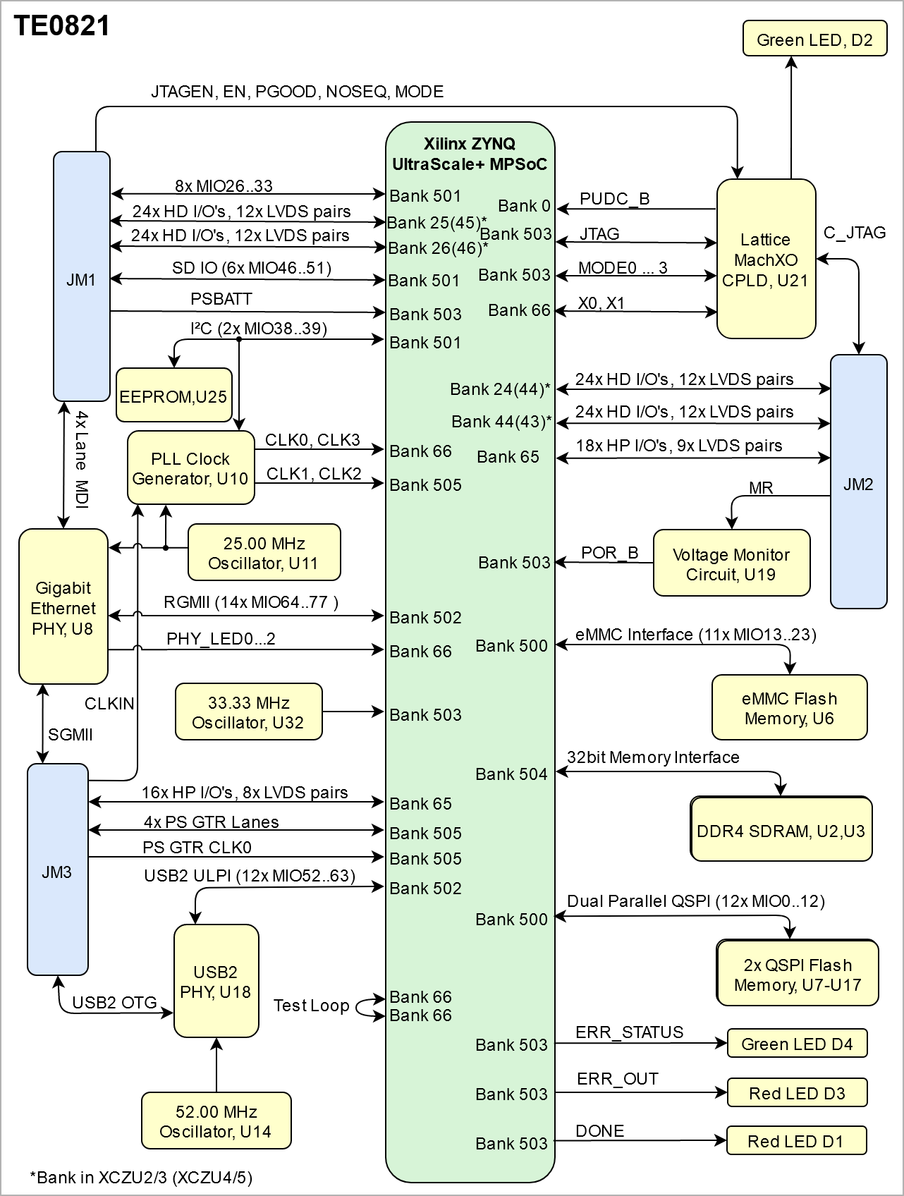
Block Diagram
| Page properties |
|---|
|
add drawIO object here.
|
...
| Scroll Title |
|---|
| anchor | Figure_OV_BD |
|---|
| title | TE0821 block diagram |
|---|
|
| Scroll Ignore |
|---|
| draw.io Diagram |
|---|
| border | false |
|---|
| |
|---|
| diagramName | TE0821_OV_BD |
|---|
| simpleViewer | false |
|---|
| width | |
|---|
| links | auto |
|---|
| tbstyle | hidden |
|---|
| diagramDisplayName | |
|---|
| lbox | true |
|---|
| diagramWidth | 641 |
|---|
| revision | 819 |
|---|
|
|
| Scroll Only |
|---|
|
|
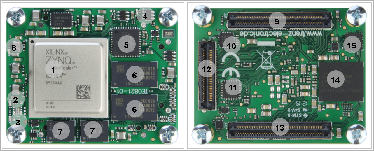
Main Components
...
| Scroll Title |
|---|
| anchor | Figure_OV_MC |
|---|
| title | TE0821 main components |
|---|
|
| Scroll Ignore |
|---|
| draw.io Diagram |
|---|
| border | false |
|---|
| |
|---|
| diagramName | TE0821_OV_MC |
|---|
| simpleViewer | false |
|---|
| width | |
|---|
| links | auto |
|---|
| tbstyle | hidden |
|---|
| diagramDisplayName | |
|---|
| lbox | true |
|---|
| diagramWidth | 641 |
|---|
| revision | 89 |
|---|
|
|
| Scroll Only |
|---|
|
|
- Xilinx Zynq ZYNQ UltraScale+ XCZU3EGMPSoC, U1
- Red LED (ERR_OUT), D3
- Green LED (ERR_STATUS), D4
- Red LED (DONE), D1
- 10/100/1000 Mbps energy efficient ethernet transceiverEnergy Efficient Ethernet Transceiver, U8
- 8Gb DDR4, U2-U3
- 512 Mbit QSPI flash memory, U7-U17
- Green User LED, D2
- B2B connector Samtec Razor Beam, JM1
- Green User LED, D2
- Programmable clock generator, U10
- USB2.0 Transceiver, U18
- B2B connector Samtec Razor Beam, JM3
- B2B connector Samtec Razor Beam, JM2
- 8 GByte eMMC memory, U6
- Lattice Semiconductor MachXO2 System Controller CPLD, U21
...
| Scroll Title |
|---|
| anchor | Table_OV_IDS |
|---|
| title | Initial delivery state of programmable devices on the module |
|---|
|
| Scroll Table Layout |
|---|
| orientation | portrait |
|---|
| sortDirection | ASC |
|---|
| repeatTableHeaders | default |
|---|
| style | |
|---|
| widths | |
|---|
| sortByColumn | 1 |
|---|
| sortEnabled | false |
|---|
| cellHighlighting | true |
|---|
|
Storage device name | Content | Notes |
|---|
Dual QSPI Flash Memory | Not programmed |
| eMMC Memory | Not programmed |
| | DDR4 SDRAM | Not programmed |
| | Programmable Clock Generator | Not programmed |
| | CPLD (LCMXO2-256HC) | ???? FirmwareProgrammed | TE0821 CPLD |
|
Configuration Signals
...
| Scroll Title |
|---|
| anchor | Table_OV_BP |
|---|
| title | Boot process. |
|---|
|
| Scroll Table Layout |
|---|
| orientation | portrait |
|---|
| sortDirection | ASC |
|---|
| repeatTableHeaders | default |
|---|
| style | |
|---|
| widths | |
|---|
| sortByColumn | 1 |
|---|
| sortEnabled | false |
|---|
| cellHighlighting | true |
|---|
|
MODE Pin | Boot Mode |
|---|
| LowHigh | QSPI* | | HighLow | SD Card* |
|
*changable also with other CPLD Firmware: TE0821 CPLD.
| Scroll Title |
|---|
| anchor | Table_OV_RST |
|---|
| title | Reset process. |
|---|
|
| Scroll Table Layout |
|---|
| orientation | portrait |
|---|
| sortDirection | ASC |
|---|
| repeatTableHeaders | default |
|---|
| style | |
|---|
| widths | |
|---|
| sortByColumn | 1 |
|---|
| sortEnabled | false |
|---|
| cellHighlighting | true |
|---|
|
Signal | B2B | I/O | Note |
|---|
EN | JM1-28 | Input | CPLD Enable Pin |
|
Please refer to the TE0821 CPLD-Bootmode.
Signals, Interfaces and Pins
...
| Scroll Title |
|---|
| anchor | Table_SIP_B2B |
|---|
| title | General PL I/O to B2B connectors information |
|---|
|
| Scroll Table Layout |
|---|
| orientation | portrait |
|---|
| sortDirection | ASC |
|---|
| repeatTableHeaders | default |
|---|
| style | |
|---|
| widths | |
|---|
| sortByColumn | 1 |
|---|
| sortEnabled | false |
|---|
| cellHighlighting | true |
|---|
|
| FPGA Bank | Type | B2B Connector | I/O Signal Count | Voltage Level | Notes |
|---|
| 24 | HD | JM2 | 24x I/O, 12x LVDS Pairs | Variable | Max voltage 3.3V | | 25 | HD | JM1 | 24x I/O, 12x LVDS Pairs | Variable | Max voltage 3.3V | | 26 | HD | JM1 | 24x I/O, 12x LVDS Pairs | Variable | Max voltage 3.3V | | 44 | HD | JM2 | 24x I/O, 12x LVDS Pairs | Variable | Max voltage 3.3V | | 65 | HP | JM2 | 18x I/O, 9x LVDS Pairs | Variable | Max voltage 1.8V | 65 | HP | JM3 | 16x I/O, 8x LVDS Pairs | Variable | Max voltage 1.8V | | 505 | GTR | JM3 | 16x I/O, 8x LVDS Pairs | - | 4x lanes | | 505 | GTR CLK | JM3 | 1x Diff Clock | - |
| 501 | MIO | JM1 | 15 I/O | 3.3V |
|
|
...
| Scroll Title |
|---|
| anchor | Table_SIP_TPs |
|---|
| title | Test Points Information |
|---|
|
| Scroll Table Layout |
|---|
| orientation | portrait |
|---|
| sortDirection | ASC |
|---|
| repeatTableHeaders | default |
|---|
| style | |
|---|
| widths | |
|---|
| sortByColumn | 1 |
|---|
| sortEnabled | false |
|---|
| cellHighlighting | true |
|---|
|
| Test Point | Signal | Connected to | Notes |
|---|
| 1 | I2C_SCL | EEPROM, U25 |
| | 2 | I2C_SDA | EEPROM, U25 |
| | 3 | SRST_B | FPGA Bank 503 | PSCONFIG | | 4 | PS_CLK | FPGA Bank 503 | PSCONFIG | | 5 | PROG_B | FPGA Bank 503 | PSCONFIG | | 6 | INIT_B | FPGA Bank 503 | PSCONFIG | | 7 | DONE | Red LED, D1 |
| | 8 | PS_LP0V85 | Voltage Regulator, U12 |
| | 9 | DDR_2V5 | Voltage Regulator, U4 |
| | 10 | PS_AVCC | Voltage Regulator, U9 |
| | 11 | DDR_1V2 | Voltage Regulator, U15 |
| | 12 | PS_AVTT | Voltage Regulator, U3U13 |
| | 13 | PS_FP0V85 | Voltage Regulator, U26 |
| | 14 | POR_B | Voltage Translator, U19 |
| | 15 | PS_PLL | Voltage Regulator, U23 |
| | 16 | PL_VCCINT | Voltage Regulator, U5 |
|
|
...
| Scroll Title |
|---|
| anchor | Table_OBP |
|---|
| title | On board peripherals |
|---|
|
| Scroll Table Layout |
|---|
| orientation | portrait |
|---|
| sortDirection | ASC |
|---|
| repeatTableHeaders | default |
|---|
| style | |
|---|
| widths | |
|---|
| sortByColumn | 1 |
|---|
| sortEnabled | false |
|---|
| cellHighlighting | true |
|---|
|
|
Quad SPI Flash Memory
...
| Scroll Title |
|---|
| anchor | Table_OBP_PCLK |
|---|
| title | Programmable Clock Generator Inputs and Outputs |
|---|
|
| Scroll Table Layout |
|---|
| orientation | portrait |
|---|
| sortDirection | ASC |
|---|
| repeatTableHeaders | default |
|---|
| sortByColumn | 1 |
|---|
| sortEnabled | false |
|---|
| cellHighlighting | true |
|---|
|
| U25 Pin | Signal | Connected to | Direction | Note |
|---|
IN0..1 | CLK_IN | JM3 | IN |
| | IN2 | CLK_25M | Oscillator, U11 | IN |
| | SCL | I2C_SCL | EEPROM,U25 | INOUT |
| | SDA | I2C_SDA | EEPROM,U25 | INOUT |
| | CLK0 | CLK0 | JM3 | OUT |
| | CLK1 | B505_CLK3 | FPGA Bank 505 | IN |
| | CLK2 | B505_CLK1 | FPGA Bank 505 | IN |
| | CLK3 | CLK3_N |
| IN |
|
|
...
| Scroll Title |
|---|
| anchor | Figure_PWR_PD |
|---|
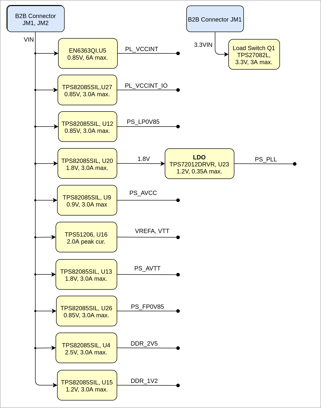
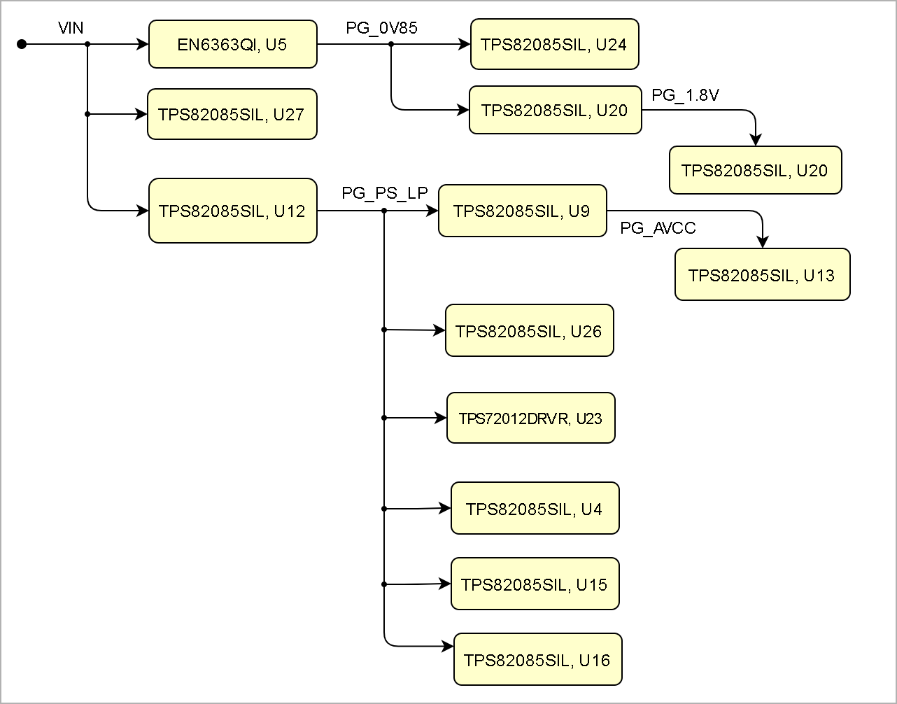
| title | Power DistributionDistribution |
|---|
|
| Scroll Ignore |
|---|
| scroll-pdf | true |
|---|
| scroll-office | true |
|---|
| scroll-chm | true |
|---|
| scroll-docbook | true |
|---|
| scroll-eclipsehelp | true |
|---|
| scroll-epub | true |
|---|
| scroll- |
|---|
| ignore | | draw.io Diagram |
|---|
| border | false |
|---|
| |
|---|
| diagramName | TE0821_PWR_PD |
|---|
| simpleViewer | false |
|---|
| width | |
|---|
| links | auto |
|---|
| tbstyle | hidden |
|---|
| diagramDisplayName | |
|---|
| lbox | true |
|---|
| diagramWidth | 641 |
|---|
| revision | 5 |
|---|
|
|
| Scroll Only |
|---|
|
|
...
| Scroll Title |
|---|
| anchor | Figure_PWR_PS |
|---|
| title | Power Sequency |
|---|
|
| Scroll Ignore |
|---|
| draw.io Diagram |
|---|
| border | false |
|---|
| |
|---|
| diagramName | TE0821_PWR_PS |
|---|
| simpleViewer | false |
|---|
| width | |
|---|
| links | auto |
|---|
| tbstyle | hidden |
|---|
| diagramDisplayName | |
|---|
| lbox | true |
|---|
| diagramWidth | 641 |
|---|
| revision | 78 |
|---|
|
|
| Scroll Only |
|---|
|
|
Power Rails
| Scroll Title |
|---|
| anchor | Table_PWR_PR |
|---|
| title | Module power rails. |
|---|
|
| Scroll Table Layout |
|---|
| orientation | portrait |
|---|
| sortDirection | ASC |
|---|
| repeatTableHeaders | default |
|---|
| style | |
|---|
| widths | |
|---|
| sortByColumn | 1 |
|---|
| sortEnabled | false |
|---|
| cellHighlighting | true |
|---|
|
| Power Rail Name | B2B JM1 Pin | B2B JM2 Pin | B2B JM3 Pin | Direction | Notes |
|---|
| VIN | 1, 3, 5 | 2, 4, 6, 8 | - | Input | Supply voltage from the carrier board | | 3.3V | - | 10, 12 | - | Output | Internal 3.3V voltage level | | VCCO_HD25_26 | 9,11 |
| - | Input | 0 to 3.3V Voltage | | 3.3VIN | 13, 15 | - | - | Input | Supply voltage from the carrier board | | 1.8V | 39 | - | - | Output | Internal 1.8V voltage level | | JTAG VREF | - | 91 | - | Output | JTAG reference voltage.
Attention: Net name on schematic is "3.3VIN" | | VCCO_HD24_ |
64High performance I/O bank voltage| 0 to 3.3V Voltage | | VCCO_65 | - | 5 | - | Input |
High performance I/O bank voltage | | 0 to 1.8V Voltage | | PSBATT | 79 | - |
VCCO_66 | 9, 11High performance I/O bank voltage
|
Bank Voltages
| Scroll Title |
|---|
| anchor | Table_PWR_BV |
|---|
| title | Zynq SoC bank voltages. |
|---|
|
| Scroll Table Layout |
|---|
| orientation | portrait |
|---|
| sortDirection | ASC |
|---|
| repeatTableHeaders | default |
|---|
| style | |
|---|
| widths | |
|---|
| sortByColumn | 1 |
|---|
| sortEnabled | false |
|---|
| cellHighlighting | true |
|---|
|
| FPGA Bank | Schematic | Voltage | Note |
|---|
| Bank 24 HD | VCCO_HD24_2444 | Variable | Max voltage 3.3V | | Bank 25 HD | VCCO_HD25_26 | Variable | Max voltage 3.3V | | Bank 26 HD | VCCO_HD25_26 | Variable | Max voltage 3.3V | | Bank 44 HD | VCCO_HD24_44 | Variable | Max voltage 3.3V | | Bank 64 HP | VCCO_64 | N.C | Not Connected | | Bank 65 HP | VCCO_65 | Variable | Max voltage 1.8V | | Bank 66 HP | VCCO_66 | 1.8V |
| | Bank 500 PSMIO | VCCO_PSIO0_500 | 1.8V |
| Bank 501 PSMIO | VCCO_PSIO1_501 | 3.3V |
| | Bank 502 PSMIO | VCCO_PSIO2_502 | 1.8V |
| | Bank 503 PSCONFIG | VCCO_PSIO3_503 | 1.8V |
| | Bank 504 PSDDR | DDR_1V2 | 1.2V |
|
|
Board to Board Connectors
| Page properties |
|---|
|
- This section is optional and only for modules.
use "include page" macro and link to the general B2B connector page of the module series, For example: 6 x 6 SoM LSHM B2B Connectors
| Include Page |
|---|
| PD:6 x 6 SoM LSHM B2B ConnectorsPD: |
|---|
| 6 x 6 SoM LSHM B2B Connectors |
|---|
|
|
| Include Page |
|---|
| PD:4 x 5 SoM LSHM B2B ConnectorsPD: |
|---|
| 4 x 5 SoM LSHM B2B Connectors |
|---|
|
...
| Scroll Title |
|---|
| anchor | Table_TS_AMR |
|---|
| title | PS absolute maximum ratings |
|---|
|
| Scroll Table Layout |
|---|
| orientation | portrait |
|---|
| sortDirection | ASC |
|---|
| repeatTableHeaders | default |
|---|
| style | |
|---|
| widths | |
|---|
| sortByColumn | 1 |
|---|
| sortEnabled | false |
|---|
| cellHighlighting | true |
|---|
|
| Description | Min | Max | Unit | Notes |
|---|
VIN supply voltage | -0.3 | 7 | V | See EN6347QI and TPS82085SIL datasheets3.3VIN supply | | 3.3VIN supply voltage | -0.1 | 3.630 | V | Xilinx DS925 and TPS27082L datasheet | | PS I/O supply voltage, VCCO_PSIO | -0.5 | 3.630 | V | Xilinx document DS925 | | PS I/O input voltage | -0. | 13.6305 | VCCO_PSIO + 0.55 | V | Xilinx document DS925 | | HP | DS925 and TPS27082L datasheetPS I/O bank supply voltage, VCCO | _PSIO | -0.5 | 32. | 6300 | V | Xilinx document DS925 | PS | HP I/O bank input voltage | -0. | 555 | VCCO | _PSIO + 0.55 | V | Xilinx document DS925HP | | HD I/O bank supply voltage, VCCO | -0.5 | 23. | 04 | V | Xilinx document DS925 | HP | HD I/O bank input voltage | -0.55 | VCCO + 0.55 | V | Xilinx document DS925 | | PS GTR reference clocks absolute input voltage | -0.5 | 1.1 | V | Xilinx document DS925 | | PS GTR absolute input voltage | -0.5 | 1.1 | V | Xilinx document DS925 | Voltage on SC CPLD pins | -0.5 | 3.75 | V | Lattice Semiconductor MachXO2 datasheet | Storage temperature | -40 | +85 | °C | See eMMC datasheet |
|
...
| Scroll Title |
|---|
| anchor | Table_TS_ROC |
|---|
| title | Recommended operating conditions. |
|---|
|
| Scroll Table Layout |
|---|
| orientation | portrait |
|---|
| sortDirection | ASC |
|---|
| repeatTableHeaders | default |
|---|
| style | |
|---|
| widths | |
|---|
| sortByColumn | 1 |
|---|
| sortEnabled | false |
|---|
| cellHighlighting | true |
|---|
|
| Parameter | Min | Max | Units | Reference Document |
|---|
| VIN supply voltage | 3.3 | 6 | V | See TPS82085S datasheet | | 3.3VIN supply voltage | 3.3 | 3.465 | V | See LCMXO2-256HC, Xilinx DS925 datasheet | | PS I/O supply voltage, VCCO_PSIO | 1.710 | 3.465 | V | Xilinx document DS925 | | PS I/O input voltage | –0.20 | VCCO_PSIO + 0.20 | V | Xilinx document DS925 | | HP I/O banks supply voltage, VCCO_PSIO | 10.710950 | 31.4659 | V | Xilinx document DS925 | | PS HP I/O banks input voltage | –0-0.20 | VCCO _PSIO + 0.20 | V | Xilinx document DS925HP | | HD I/O banks supply voltage, VCCO | 01. | 95014 | 13. | 94 | V | Xilinx document DS925 | HP | HD I/O banks input voltage | -0.20 | VCCO + 0.20 | V | Xilinx document DS925 | | Voltage on SC CPLD pins | -0.3 | 3.6 | V | Lattice Semiconductor MachXO2 datasheet | | Operating Temperature Range | 0 | 85 | °C | Xilinx document DS925, extended grade Zynq temperarure range |
|
...
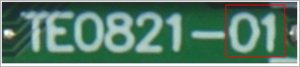
| Scroll Title |
|---|
| anchor | Figure_RV_HRN |
|---|
| title | Board hardware revision number. |
|---|
|
| Scroll Ignore |
|---|
| draw.io Diagram |
|---|
| border | false |
|---|
| |
|---|
| diagramName | TE0821_RV_HRN |
|---|
| simpleViewer | false |
|---|
| width | |
|---|
| links | auto |
|---|
| tbstyle | hidden |
|---|
| diagramDisplayName | |
|---|
| lbox | true |
|---|
| diagramWidth | 326 |
|---|
| revision | 34 |
|---|
|
|
| Scroll Only |
|---|
|
|
Document Change History
...
| Scroll Title |
|---|
| anchor | Table_RH_DCH |
|---|
| title | Document change history. |
|---|
|
| Scroll Table Layout |
|---|
| orientation | portrait |
|---|
| sortDirection | ASC |
|---|
| repeatTableHeaders | default |
|---|
| style | |
|---|
| widths | |
|---|
| sortByColumn | 1 |
|---|
| sortEnabled | false |
|---|
| cellHighlighting | true |
|---|
|
| Date | Revision | Contributor | Description |
|---|
| Page info |
|---|
| infoType | Modified date |
|---|
| dateFormat | yyyy-MM-dd |
|---|
| type | Flat |
|---|
|
| | Page info |
|---|
| infoType | Current version |
|---|
| prefix | v. |
|---|
| type | Flat |
|---|
| showVersions | false |
|---|
|
| | Page info |
|---|
| infoType | Modified by |
|---|
| type | Flat |
|---|
| showVersions | false |
|---|
|
| | | 2021-07-05 | v.61 | John Hartfiel | Update download Link - Update Change history
| | 2021-06-07 | v.59 | Vadim Yunitski | | | 2020-07-15 | v.50 | Pedram Babakhani | | -- | all | | Page info |
|---|
| infoType | Modified users |
|---|
| type | Flat |
|---|
| showVersions | false |
|---|
|
| |
|
...