...
| Scroll Title |
|---|
| anchor | Figure_OV_BD |
|---|
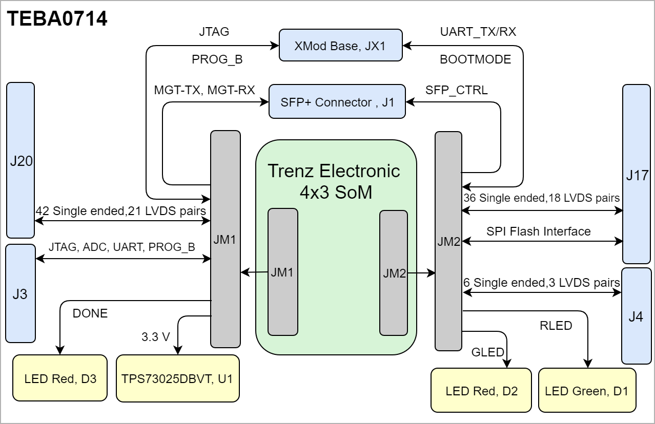
| title | TEBA0714 block diagram |
|---|
|
| Scroll Ignore |
|---|
| draw.io Diagram |
|---|
| border | false |
|---|
| viewerToolbar | true |
|---|
| |
|---|
| fitWindow | false |
|---|
| diagramDisplayName | |
|---|
| lbox | true |
|---|
| revision | 912 |
|---|
| diagramName | TEBA0714_OV_BD |
|---|
| simpleViewer | false |
|---|
| width | |
|---|
| links | auto |
|---|
| tbstyle | hidden |
|---|
| diagramWidth | 639 |
|---|
|
|
| Scroll Only |
|---|
 |
|
...
| Scroll Title |
|---|
| anchor | Table_SIP_JTG |
|---|
| title | JTAG pins connection |
|---|
|
| Scroll Table Layout |
|---|
| orientation | portrait |
|---|
| sortDirection | ASC |
|---|
| repeatTableHeaders | default |
|---|
| style | |
|---|
| widths | |
|---|
| sortByColumn | 1 |
|---|
| sortEnabled | false |
|---|
| cellHighlighting | true |
|---|
|
| XMOD Header Pin | B2B Connector | Connected to | Note |
|---|
| A | JM2-97 | B14_L25 | UART Transfer | | B | JM2-99 | B14_L0 | UART Receive | | E | JM2-100 | BOOTMODE |
| | G | JM1-94 | PROG_B |
| | C | JM1-90 | TCK |
| | D | JM1-86 | TDI |
| | F | JM1-88 | TDO |
| | H | JM1-92 | TMS |
| | 3.3V | JM1-97,99 | 3.3V |
| | VIO | JM2-53 | V_CFG |
|
...
The DIP-switch S2 on Xmod Adapter TE0790 must be set as the following table.
| Scroll Title |
|---|
| anchor | Table_SIP_SFP+XMODS2 |
|---|
| title | SFP+ Connector InformationJTAG pins connection |
|---|
|
| Scroll Table Layout |
|---|
| orientation | portrait |
|---|
| sortDirection | ASC |
|---|
| repeatTableHeaders | default |
|---|
| style | |
|---|
| widths | |
|---|
| sortByColumn | 1 |
|---|
| sortEnabled | false |
|---|
| cellHighlighting | true |
|---|
|
PinConnected toNotesVCCR3.3V| Description |
|---|
| 1 | Normal mode | Adapter board CPLD update mode | ON | Update Mode JTAG access to SC CPLD only | | 2 | Do not use (illegal setting) | Normal mode | OFF | Must be in OFF state always. | | 3 | VIO connected to 3.3V | Power VIO from pin header J2 | OFF | User I/O Voltage | | 4 | Power 3.3V from USB | Power 3.3V from pin header J2 | OFF | Power on-board peripherals (FTDI chip & SC CPLD, ...) |
|
The voltages 3.3V (VCC) and VIO (variable SC CPLD I/O-voltage) should be configured by the DIP-switches S2-3 and S2-4 as the following.
| Scroll Title |
|---|
| anchor | Table_SIP_XMODS3/4 |
|---|
| title | JTAG pins connection |
|---|
|
| Scroll Table Layout |
|---|
| orientation | portrait |
|---|
| sortDirection | ASC |
|---|
| repeatTableHeaders | default |
|---|
| style | |
|---|
| widths | |
|---|
| sortByColumn | 1 |
|---|
| sortEnabled | false |
|---|
| cellHighlighting | true |
|---|
|
| S2-3 | S2-4 | 3.3V (VCC) Pin 5 | VIO Pin 6 | Description |
|---|
| OFF | OFF | 3.3V from base (input**) | VIO from base (input**) | 3.3V (pin 5) and VIO (pin 6) sourced from base | | OFF | ON | 3.3V from USB* (output**) | VIO from base (input**) | VIO sourced from base by Pin 6 | | ON | OFF | 3.3V from base (input**) | 3.3V from base (input**) | VIO and 3.3V source by base (Pin 5 and Pin 6 are shorted and both must be sourced by 3.3V) | | ON | ON | 3.3V from USB* (output**) | 3.3V from USB* (output**) | 3.3V (pin 5) and VIO (pin 6) sourced USB (Pin 5 and Pin 6 are shorted and both are 3.3V) |
|
SFP+ Connector
| Scroll Title |
|---|
| anchor | Table_SIP_SFP+ |
|---|
| title | SFP+ Connector Information |
|---|
|
| Scroll Table Layout |
|---|
| orientation | portrait |
|---|
| sortDirection | ASC |
|---|
| repeatTableHeaders | default |
|---|
| style | |
|---|
| widths | |
|---|
| sortByColumn | 1 |
|---|
| sortEnabled | false |
|---|
| cellHighlighting | true |
|---|
|
| Pin | Connected to | Notes |
|---|
| VCCR | 3.3V |
| | VCCT | 3.3V |
| | VREF | GND |
| | TD+/TD- | VCCT | 3.3V | VREF | GND | TD+/TD- | MGT TX | MGT Lane | | RD+/RD- | MGT RX | MGT Lane | | TX/FAULT | SFP0_TX_FAUL | SFP_CTRL | | TX/DISABLE | SFP0_TX_DIS | SFP_CTRL | | MOD-DEF2 | SFP0_SDA | SFP_CTRL | | MOD-DEF1 | SFP0_SCL | SFP_CTRL | | MOD-DEF0 | SFP0_MT_DEF0 | SFP_CTRL | | RS0/RS1 | SFP0_RS0_1 | SFP_CTRL | | LOS | SFP0_LOS | SFP_CTRL |
|
...
| Scroll Title |
|---|
| anchor | Table_OBP_LED |
|---|
| title | On-board LEDs |
|---|
|
| Scroll Table Layout |
|---|
| orientation | portrait |
|---|
| sortDirection | ASC |
|---|
| repeatTableHeaders | default |
|---|
| style | |
|---|
| widths | |
|---|
| sortByColumn | 1 |
|---|
| sortEnabled | false |
|---|
| cellHighlighting | true |
|---|
|
| Designator | Color | Connected to | Active Level | Note |
|---|
| D1 | Green | GLED | Active LowHigh |
| | D2 | Red | RLED | Active High |
| | D3 | Red | DONE | Active HighLow |
|
|
Power and Power-On Sequence
...