| Page properties |
|---|
|
Template Revision 2.12
- Module: TRM Name always "TE Series Name" +TRM
Example: "TE0728 TRM" - Carrier: TRM Name usually "TEB Series Name" +TRM
Example: "TEB0728 TRM"
|
| HTML |
|---|
<!-- tables have all same width (web max 1200px and pdf full page(640px), flexible width or fix width on menu for single column can be used as before) -->
<style>
.wrapped{
  width: 100% !important;
  max-width: 1200px !important;
 }
</style> |
| Page properties |
|---|
|
Important General Note:
|
| Page properties |
|---|
|
----------------------------------------------------------------------- |
| Page properties |
|---|
|
Note for Download Link of the Scroll ignore macro: |
| Scroll pdf ignore |
|---|
Table of Contents |
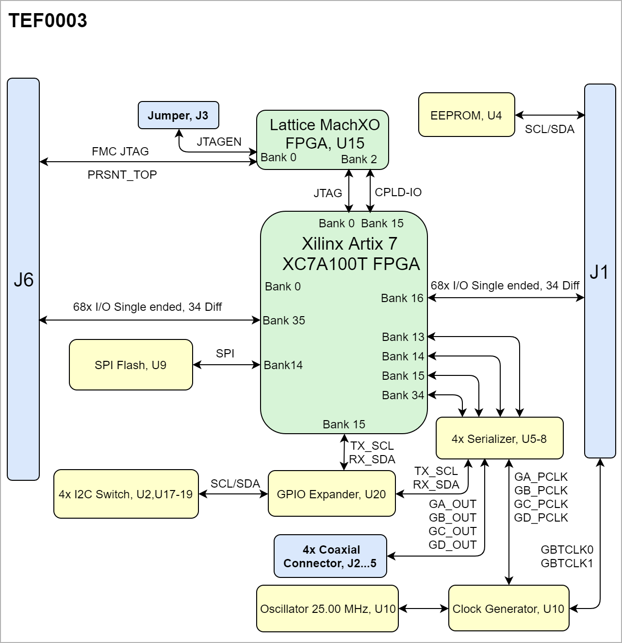
Overview
The Trenz Electronic TEF0003 is a FPGA Mezzanine Card (FMC) integrated with an Artix 7 FPGA, 512 Mb Flash Memory.
Refer to http://trenz.org/tef0003-info for the current online version of this manual and other available documentation.
Key Features
| Page properties |
|---|
|
Note:
'description: Important components and connector or other Features of the module
→ please sort and indicate assembly options Key Features' must be split into 6 main groups: - FPGA/Module
- Package:
- Speed:
- Temperature:
- RAM/Storage
- On Board
- Interface
- E.g. ETH, USB, B2B, Display port
- Power
- E.g. Input supply voltage
- Dimension
|
- FPGA: Xilinx Artix 7 (XC7A100T)
- Package: FGG484 (Compatible with
- Speed: -1 (Slowest)
- Temperature: Industrial Grade (–40°C to +100°C)
- RAM/Storage:
- 1x NOR SPI FLASH (128M x 4)
- 1x EEPROM (16K x 8)
- On Board:
- 4x Deserializer IC (3.12 Gbps)
- 4x I2C and SMBus I/O Expander
- 1x Programable Clock Generator
- 1x Clock Generator
- Interface:
- 2x VITA 57 SEAM/SEAF Series
- 4x Coaxial Connectors
- Power:
- 4x Voltage Regulators
- 3.3 Supply Voltage
- Dimension:
Block Diagram
| Page properties |
|---|
|
add drawIO object here.
|
| Scroll Title |
|---|
| anchor | Figure_OV_BD |
|---|
| title | TEF0003 block diagram |
|---|
|
| Scroll Ignore |
|---|
| draw.io Diagram |
|---|
| border | false |
|---|
| viewerToolbar | true |
|---|
| |
|---|
| fitWindow | false |
|---|
| diagramDisplayName | |
|---|
| lbox | true |
|---|
| revision | 12 |
|---|
| diagramName | TEF0003_OV_BD |
|---|
| simpleViewer | false |
|---|
| width | |
|---|
| links | auto |
|---|
| tbstyle | hidden |
|---|
| diagramWidth | 641 |
|---|
|
|
| Scroll Only |
|---|
|
|
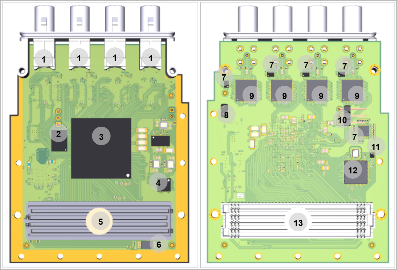
Main Components
| Page properties |
|---|
|
Notes : - Picture of the PCB (top and bottom side) with labels of important components
- Add List below
|
| Scroll Title |
|---|
| anchor | Figure_OV_MC |
|---|
| title | TEF0003 main components |
|---|
|
| Scroll Ignore |
|---|
| draw.io Diagram |
|---|
| border | false |
|---|
| viewerToolbar | true |
|---|
| |
|---|
| fitWindow | false |
|---|
| diagramDisplayName | |
|---|
| lbox | true |
|---|
| revision | 7 |
|---|
| diagramName | TEF0003_OV_MC |
|---|
| simpleViewer | false |
|---|
| width | |
|---|
| links | auto |
|---|
| tbstyle | hidden |
|---|
| diagramWidth | 641 |
|---|
|
|
| Scroll Only |
|---|
|
|
- Coaxial Connectors, J2-5
- SPI Flash, U9
- Xilinx Artix 7 FPGA, U1
- Lattice MachXO FPGA, U15
- FMC Adapter, J1
- EEPROM, U4
- I2C Switches, U2, U17-20
- Jumper, J7
- Serializer, U5-8
- Connector Header, J8
- Oscillator 25MHz, U11
- Programmable Clock Generator, U10
- FMC Adapter, J6
Initial Delivery State
| Page properties |
|---|
|
Notes : Only components like EEPROM, QSPI flash and DDR3 can be initialized by default at manufacture. If there is no components which might have initial data ( possible on carrier) you must keep the table empty |
| Scroll Title |
|---|
| anchor | Table_OV_IDS |
|---|
| title | Initial delivery state of programmable devices on the module |
|---|
|
| Scroll Table Layout |
|---|
| orientation | portrait |
|---|
| sortDirection | ASC |
|---|
| repeatTableHeaders | default |
|---|
| sortByColumn | 1 |
|---|
| sortEnabled | false |
|---|
| cellHighlighting | true |
|---|
|
Storage device name | Content | Notes |
|---|
SPI Flash | Not programmed |
| | EEPROM | Not Programmed |
| | Clock Generator | Programmed |
|
|
Configuration Signals
| Page properties |
|---|
|
- Overview of Boot Mode, Reset, Enables.
|
| Scroll Title |
|---|
| anchor | Table_OV_BP |
|---|
| title | Boot process. |
|---|
|
| Scroll Table Layout |
|---|
| orientation | portrait |
|---|
| sortDirection | ASC |
|---|
| repeatTableHeaders | default |
|---|
| sortByColumn | 1 |
|---|
| sortEnabled | false |
|---|
| cellHighlighting | true |
|---|
|
MODE Signal State M[2:0] | Boot Mode | Note |
|---|
110 | Master SPI | It is Fixed |
|
| Scroll Title |
|---|
| anchor | Table_OV_RST |
|---|
| title | Reset Process. |
|---|
|
| Scroll Table Layout |
|---|
| orientation | portrait |
|---|
| sortDirection | ASC |
|---|
| repeatTableHeaders | default |
|---|
| sortByColumn | 1 |
|---|
| sortEnabled | false |
|---|
| cellHighlighting | true |
|---|
|
Signal | Description | Note |
|---|
PRSNT_TOP | Lattice MachXO Configuration Pin |
| | PROG_B | Artix 7 Configuration Pin | Connected to 1.8 |
|
Signals, Interfaces and Pins
| Page properties |
|---|
|
Notes : - For carrier or stand-alone boards use subsection for every connector type (add designator on description, not on the subsection title), for example:
- For modules which needs carrier use only classes and refer to B2B connector if more than one is used, for example
|
FMC Connectors
FPGA bank number and number of I/O signals connected to the FMC Connectors J1 and J6 which are located on top and bottom of the board.
| Scroll Title |
|---|
| anchor | Table_SIP_FMC |
|---|
| title | General PL I/O to FMC Connectors information |
|---|
|
| Scroll Table Layout |
|---|
| orientation | portrait |
|---|
| sortDirection | ASC |
|---|
| repeatTableHeaders | default |
|---|
| sortByColumn | 1 |
|---|
| sortEnabled | false |
|---|
| cellHighlighting | true |
|---|
|
| FPGA | FPGA Bank | Connector Designator | I/O Signal Count | Voltage Level | Notes |
|---|
| Artix 7, U1 | 16 | J1B | 68 Single Ended, 34 Differential | 1.8V |
| | 35 | J6B | 68 Single Ended, 34 Differential | 1.8V |
| | Lattice MachXO, U | 0 | J1F | 4 Single Ended | 3.3V | CPLD | | 0 | J6F | 4 Single Ended | 3.3V | CPLD |
|
Coaxial Connectors
| Scroll Title |
|---|
| anchor | Table_SIP_Coaxial |
|---|
| title | Coaxial Connectors information |
|---|
|
| Scroll Table Layout |
|---|
| orientation | portrait |
|---|
| sortDirection | ASC |
|---|
| repeatTableHeaders | default |
|---|
| sortByColumn | 1 |
|---|
| sortEnabled | false |
|---|
| cellHighlighting | true |
|---|
|
| Designator | Schematic | Connected to | Notes |
|---|
| J2 | GA_OUT | Serializer, U5 | Output Serializer | | J3 | GB_OUT | Serializer, U6 | Output Serializer | | J4 | GC_OUT | Serializer, U7 | Output Serializer |
| GD_OUT | Serializer, U8 | Output Serializer |
|
JTAG Interface
The Lattice MachXO (U15) is available to meet the requirement of a CPLD, JTAG access to the MachXO is available through FMC Adapter J6. JTAG access to the Artix 7(U1) is available via MachXO, Bank 2.
| Scroll Title |
|---|
| anchor | Table_SIP_CPLDJTG |
|---|
| title | CPLD JTAG pins connection |
|---|
|
| Scroll Table Layout |
|---|
| orientation | portrait |
|---|
| sortDirection | ASC |
|---|
| repeatTableHeaders | default |
|---|
| sortByColumn | 1 |
|---|
| sortEnabled | false |
|---|
| cellHighlighting | true |
|---|
|
JTAG Signal | B2B Connector |
|---|
| FMC_TMS | J6F-TCK | | FMC_TDI_TOP | J6F-J1-TDI | | FMC_TDO_TOP | J6F-TDO | | FMC_TCK | J6F-TCK | | JTAGEN | Pulled down |
|
| Scroll Title |
|---|
| anchor | Table_SIP_JTG |
|---|
| title | JTAG pins connection |
|---|
|
| Scroll Table Layout |
|---|
| orientation | portrait |
|---|
| sortDirection | ASC |
|---|
| repeatTableHeaders | default |
|---|
| sortByColumn | 1 |
|---|
| sortEnabled | false |
|---|
| cellHighlighting | true |
|---|
|
JTAG Signal | Connected to | Note |
|---|
| TMS | Lattice MachXO, U15 BankArtix 7 FPGA, U1 | Bank 2 Bank 0 | | TDI | Lattice MachXO, U15 Artix 7 FPGA, U1 | Bank 2 Bank 0 | | TDO | Lattice MachXO, U15 Artix 7 FPGA, U1 | Bank 2 Bank 0 | | TCK | Lattice MachXO, U15 Artix 7 FPGA, U1 | Bank 2 Bank 0 | | INIT | Artix 7 FPGA, U1 | Connected to 1.8 |
|
On-board Peripherals
| Page properties |
|---|
|
Notes : - add subsection for every component which is important for design, for example:
- Two 100 Mbit Ethernet Transciever PHY
- USB PHY
- Programmable Clock Generator
- Oscillators
- eMMCs
- RTC
- FTDI
- ...
- DIP-Switches
- Buttons
- LEDs
|
| Page properties |
|---|
|
Notes : In the on-board peripheral table "chip/Interface" must be linked to the corresponding chapter or subsection |
| Scroll Title |
|---|
| anchor | Table_OBP |
|---|
| title | On board peripherals |
|---|
|
| Scroll Table Layout |
|---|
| orientation | portrait |
|---|
| sortDirection | ASC |
|---|
| repeatTableHeaders | default |
|---|
| sortByColumn | 1 |
|---|
| sortEnabled | false |
|---|
| cellHighlighting | true |
|---|
|
|
Quad SPI Flash Memory
| Page properties |
|---|
|
Notes : Minimum and Maximum density of quad SPI flash must be mentioned for other assembly options. |
TEF0003 is equipped with a 512Mb Serial NOR Flash (x1/x2/x4) which is provided to store an application in the SPI Flash memory in order to boot the module. The SPI Flash data is connected to Artix 7 via FPGA Bank 14.
| Scroll Title |
|---|
| anchor | Table_OBP_SPI |
|---|
| title | Quad SPI interface MIOs and pins |
|---|
|
| Scroll Table Layout |
|---|
| orientation | portrait |
|---|
| sortDirection | ASC |
|---|
| repeatTableHeaders | default |
|---|
| sortByColumn | 1 |
|---|
| sortEnabled | false |
|---|
| cellHighlighting | true |
|---|
|
| Schematic | U9 Pin | Notes |
|---|
| SPI-CS | CS |
| | SPI-CLK | CLK |
| | SPI-DQO | DI/IO0 |
| | SPI_DQ3 | HOLD/IO3 |
| | SPI-DQ2 | WP/IO2 |
| | SPI-DQ1 | DO/IO1 |
| | 1.8V | VCC |
|
|
EEPROM
A microchip serial EEPROM (U4) is provided for IPMI data. It is accessible via the LPC FMC connector J1 (SCL, SDA).
| Scroll Title |
|---|
| anchor | Table_OBP_EEP |
|---|
| title | I2C EEPROM interface MIOs and pins |
|---|
|
| Scroll Table Layout |
|---|
| orientation | portrait |
|---|
| sortDirection | ASC |
|---|
| repeatTableHeaders | default |
|---|
| sortByColumn | 1 |
|---|
| sortEnabled | false |
|---|
| cellHighlighting | true |
|---|
|
| FMC Pcam Adapter | Schematic | U4 Pin | Notes |
|---|
| J1F-SCL | FMC_SCL | SCL |
| | J1F-SDA | FMC_SDA | SDA |
| | J1F-GA0 | GA0 | A0 |
| | J1F-GA1 | GA1 | A1 |
|
|
| Scroll Title |
|---|
| anchor | Table_OBP_I2C_EEPROM |
|---|
| title | I2C address for EEPROM |
|---|
|
| Scroll Table Layout |
|---|
| orientation | portrait |
|---|
| sortDirection | ASC |
|---|
| repeatTableHeaders | default |
|---|
| sortByColumn | 1 |
|---|
| sortEnabled | false |
|---|
| cellHighlighting | true |
|---|
|
| I2C Address | Designator | Notes |
|---|
| 0x50 | U4 |
|
|
Clock Sources
| Scroll Title |
|---|
| anchor | Table_OBP_CLK |
|---|
| title | Osillators |
|---|
|
| Scroll Table Layout |
|---|
| orientation | portrait |
|---|
| sortDirection | ASC |
|---|
| repeatTableHeaders | default |
|---|
| sortByColumn | 1 |
|---|
| sortEnabled | false |
|---|
| cellHighlighting | true |
|---|
|
| Designator | Description | Frequency | Note |
|---|
| U4 | Oscillator | 25.00 MHz |
| | U10 | Programmable Clock Generator | Variable |
|
|
Programmable Clock Generator
There is a Silicon Labs I2C programmable clock generator on-board (U10) in order to generate reference clocks for the module. Programming can be done using I2C via PIN header J8. The I2C Address is 0x69.
| Scroll Title |
|---|
| anchor | Table_OBP_PCLK |
|---|
| title | Programmable Clock Generator Inputs and Outputs |
|---|
|
| Scroll Table Layout |
|---|
| orientation | portrait |
|---|
| sortDirection | ASC |
|---|
| repeatTableHeaders | default |
|---|
| sortByColumn | 1 |
|---|
| sortEnabled | false |
|---|
| cellHighlighting | true |
|---|
|
Si5345A Pin
| Signal Name / Description
| Connected To | Direction | Note |
|---|
IN0 | Reference input clock. | U11 | Input | 25.00 MHz oscillator, SiT8008BI | | IN1 | FMCT_GBTCLK0 | J6E | Input | FMC Pcam Adapter | | IN2 | FMCT_GBTCLK1 | J6E | Input | FMC Pcam Adapter | | IN3 | FMCT_CLK0 | J6E | Input | FMC Pcam Adapter | XAXB | - | GND | Input | 54.00 MHz CX3225SB | | SCLK | PLL_SCL | J8, U20 | Input | EEPROM | | SDA | PLL_SDA | J8, U20 | Input | EEPROM | | OUT0 | GA_PCLK | U5/U1 | Output | FPGA bank 15 | | OUT1 | GB_PCLK | U6/U1 | Output | FPGA bank 15 | | OUT2 | GC_PCLK | U7/U1 | Output | FPGA bank 15 | | OUT3 | GD_PCLK | U8/U1 | Output | FPGA bank 15 | | OUT4 | CLK4_P | U1H | Output |
| | OUT5 | GBTCLK0 | J1E/J6E | Output |
| | OUT6 | GBTCLK1 | J1E/J6E | Output |
| | OUT7 | GBTCLK0 | J1E | Output |
| | OUT8/OUT9 | CLK8/CLK9 | Pulled low | Output |
|
|
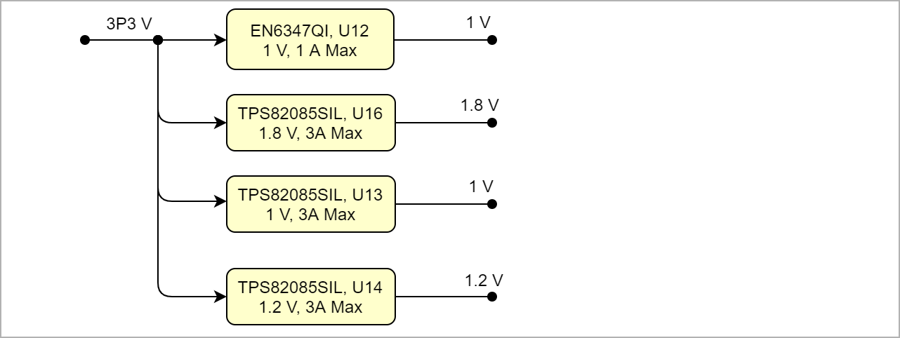
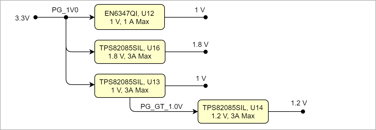
Power and Power-On Sequence
| Page properties |
|---|
|
In 'Power and Power-on Sequence' section there are three important digrams which must be drawn: - Power on-sequence
- Power distribution
- Voltage monitoring circuit
|
Power Supply
Power supply with minimum current capability of 3 A for system startup is recommended.
Power Consumption
| Scroll Title |
|---|
| anchor | Table_PWR_PC |
|---|
| title | Power Consumption |
|---|
|
| Scroll Table Layout |
|---|
| orientation | portrait |
|---|
| sortDirection | ASC |
|---|
| repeatTableHeaders | default |
|---|
| sortByColumn | 1 |
|---|
| sortEnabled | false |
|---|
| cellHighlighting | true |
|---|
|
| Power Input Pin | Typical Current |
|---|
| VIN | TBD* |
|
* TBD - To Be Determined
Power Distribution Dependencies
| Scroll Title |
|---|
| anchor | Figure_PWR_PD |
|---|
| title | Power Distribution |
|---|
|
| Scroll Ignore |
|---|
| draw.io Diagram |
|---|
| border | false |
|---|
| viewerToolbar | true |
|---|
| |
|---|
| fitWindow | false |
|---|
| diagramDisplayName | |
|---|
| lbox | true |
|---|
| revision | 7 |
|---|
| diagramName | TEF0003_PWR_PD |
|---|
| simpleViewer | false |
|---|
| width | |
|---|
| links | auto |
|---|
| tbstyle | hidden |
|---|
| diagramWidth | 641 |
|---|
|
|
| Scroll Only |
|---|
|
|
Power-On Sequence
| Scroll Title |
|---|
| anchor | Figure_PWR_PS |
|---|
| title | Power Sequency |
|---|
|
| Scroll Ignore |
|---|
| draw.io Diagram |
|---|
| border | false |
|---|
| viewerToolbar | true |
|---|
| |
|---|
| fitWindow | false |
|---|
| diagramDisplayName | |
|---|
| lbox | true |
|---|
| revision | 2 |
|---|
| diagramName | TEF0003_PWR_PS |
|---|
| simpleViewer | false |
|---|
| width | |
|---|
| links | auto |
|---|
| tbstyle | hidden |
|---|
| diagramWidth | 641 |
|---|
|
|
| Scroll Only |
|---|
|
|
Power Rails
| Scroll Title |
|---|
| anchor | Table_PWR_PR |
|---|
| title | Module power rails. |
|---|
|
| Scroll Table Layout |
|---|
| orientation | portrait |
|---|
| sortDirection | ASC |
|---|
| repeatTableHeaders | default |
|---|
| sortByColumn | 1 |
|---|
| sortEnabled | false |
|---|
| cellHighlighting | true |
|---|
|
| Power Rail Name | FMC Adapter J1G Pin | FMC Adapter J6G Pin | Direction | Notes |
|---|
| 12V | C35, C37 | C35, C37 | Input |
| | 3P3VAUX | D32 | D32 | Input |
| | 3P3V | D36, D38, D40, C39 | D36, D38, D40, C39 | Input |
| VREFA | H1 | H1 | Input |
| | VREFB | K1 | K1 | Input |
| | VIOB | J39, K40 | J39, K40 | Input |
| | VADJ | H40, G39, F40, E39 | H40, G39, F40, E39 | Input |
|
|
Bank Voltages
| Scroll Title |
|---|
| anchor | Table_PWR_BV |
|---|
| title | Zynq SoC bank voltages. |
|---|
|
| Scroll Table Layout |
|---|
| orientation | portrait |
|---|
| sortDirection | ASC |
|---|
| repeatTableHeaders | default |
|---|
| sortByColumn | 1 |
|---|
| sortEnabled | false |
|---|
| cellHighlighting | true |
|---|
|
| Schematic Name | | Notes |
|---|
| Bank 13 | VCCO_13 | 1.8 V |
| | Bank 14 | VCCO_14 | 1.8 V |
| | Bank 15 | VCCO_15 | 1.8 V |
| | Bank 16 | VCCO_16 | VADJ | 1.8 V | | Bank 34 | VCCO_34 | 1.8 V |
| | Bank 35 | VCCO_35 | VADJ | 1.8 V | | Bank 0 | VCCO_0 | 1.8 V |
|
|
Technical Specifications
Absolute Maximum Ratings
| Scroll Title |
|---|
| anchor | Table_TS_AMR |
|---|
| title | PS absolute maximum ratings |
|---|
|
| Scroll Table Layout |
|---|
| orientation | portrait |
|---|
| sortDirection | ASC |
|---|
| repeatTableHeaders | default |
|---|
| sortByColumn | 1 |
|---|
| sortEnabled | false |
|---|
| cellHighlighting | true |
|---|
|
| Symbols | Description | Min | Max | Unit |
|---|
| 12V | Input Supply Voltage | -12 | 12 | V | | T_STG | Storage Temperature | -40 | 85 | °C |
|
Recommended Operating Conditions
Operating temperature range depends also on customer design and cooling solution. Please contact us for options.
| Scroll Title |
|---|
| anchor | Table_TS_ROC |
|---|
| title | Recommended operating conditions. |
|---|
|
| Scroll Table Layout |
|---|
| orientation | portrait |
|---|
| sortDirection | ASC |
|---|
| repeatTableHeaders | default |
|---|
| sortByColumn | 1 |
|---|
| sortEnabled | false |
|---|
| cellHighlighting | true |
|---|
|
| Parameter | Min | Max | Units | Reference Document |
|---|
| 12V | 12 | 12 | V |
| | T_OPR | -40 | 85 | °C | See MT25QU512ABB8E12-0SIT (U9) datasheet. |
|
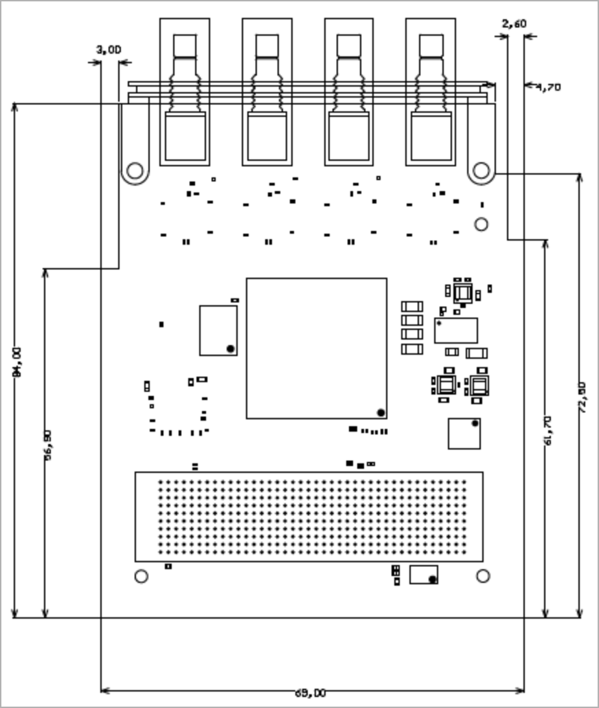
Physical Dimensions
PCB thickness: 1.56 mm.
| Scroll Title |
|---|
| anchor | Figure_TS_PD |
|---|
| title | Physical Dimension |
|---|
|
| draw.io Diagram |
|---|
| border | false |
|---|
| viewerToolbar | true |
|---|
| |
|---|
| fitWindow | false |
|---|
| diagramDisplayName | |
|---|
| lbox | true |
|---|
| revision | 5 |
|---|
| diagramName | TEF0003_TS_PD |
|---|
| aspect | 5e705185-5827-752c-089d-756568e6698b |
|---|
| simpleViewer | false |
|---|
| width | 639 |
|---|
| aspectHash | 7695f7bc00c98da1082cb1c11a0a6258edf875fc |
|---|
| links | auto |
|---|
| tbstyle | hidden |
|---|
| diagramWidth | 436 |
|---|
|
| Scroll Only |
|---|
| scroll-pdf | true |
|---|
| scroll-office | true |
|---|
| scroll-chm | true |
|---|
| scroll-docbook | true |
|---|
| scroll-eclipsehelp | true |
|---|
| scroll-epub | true |
|---|
| scroll-html | true |
|---|
| 
|
|
Currently Offered Variants
| Scroll Title |
|---|
| anchor | Table_VCP_SO |
|---|
| title | Trenz Electronic Shop Overview |
|---|
|
| Scroll Table Layout |
|---|
| orientation | portrait |
|---|
| sortDirection | ASC |
|---|
| repeatTableHeaders | default |
|---|
| sortByColumn | 1 |
|---|
| sortEnabled | false |
|---|
| cellHighlighting | true |
|---|
|
|
Revision History
Hardware Revision History
| Scroll Title |
|---|
| anchor | Table_RH_HRH |
|---|
| title | Hardware Revision History |
|---|
|
| Scroll Table Layout |
|---|
| orientation | portrait |
|---|
| sortDirection | ASC |
|---|
| repeatTableHeaders | default |
|---|
| sortByColumn | 1 |
|---|
| sortEnabled | false |
|---|
| cellHighlighting | true |
|---|
|
| Date | Revision | Changes | Documentation Link |
|---|
| 2017-06-27 | REV01 | Initial Release | REV01 |
|
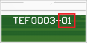
Hardware revision number can be found on the PCB board together with the module model number separated by the dash.
| Scroll Title |
|---|
| anchor | Figure_RV_HRN |
|---|
| title | Board hardware revision number. |
|---|
|
| Scroll Ignore |
|---|
| draw.io Diagram |
|---|
| border | false |
|---|
| viewerToolbar | true |
|---|
| |
|---|
| fitWindow | false |
|---|
| diagramDisplayName | |
|---|
| lbox | true |
|---|
| revision | 4 |
|---|
| diagramName | TEF0003_RV_HRN |
|---|
| simpleViewer | false |
|---|
| width | |
|---|
| links | auto |
|---|
| tbstyle | hidden |
|---|
| diagramWidth | 196 |
|---|
|
|
| Scroll Only |
|---|
|
|
Document Change History
| Page properties |
|---|
|
- Note this list must be only updated, if the document is online on public doc!
- It's semi automatically, so do following
Add new row below first Copy "Page Information Macro(date)" Macro-Preview, Metadata Version number, Author Name and description to the empty row. Important Revision number must be the same as the Wiki document revision number Update Metadata = "Page Information Macro (current-version)" Preview+1 and add Author and change description. --> this point is will be deleted on newer pdf export template - Metadata is only used of compatibility of older exports
|
| Scroll Title |
|---|
| anchor | Table_RH_DCH |
|---|
| title | Document change history. |
|---|
|
| Scroll Table Layout |
|---|
| orientation | portrait |
|---|
| sortDirection | ASC |
|---|
| repeatTableHeaders | default |
|---|
| sortByColumn | 1 |
|---|
| sortEnabled | false |
|---|
| cellHighlighting | true |
|---|
|
| Date | Revision | Contributor | Description |
|---|
| Page info |
|---|
| infoType | Modified date |
|---|
| dateFormat | yyyy-MM-dd |
|---|
| type | Flat |
|---|
|
| | Page info |
|---|
| infoType | Current version |
|---|
| prefix | v. |
|---|
| type | Flat |
|---|
| showVersions | false |
|---|
|
| | Page info |
|---|
| infoType | Modified by |
|---|
| type | Flat |
|---|
| showVersions | false |
|---|
|
| | -- | all | | Page info |
|---|
| infoType | Modified users |
|---|
| type | Flat |
|---|
| showVersions | false |
|---|
|
| |
|
Disclaimer
| Include Page |
|---|
| IN:Legal Notices |
|---|
| IN:Legal Notices |
|---|
|