...
| Scroll Title |
|---|
| anchor | Figure_OV_BD |
|---|
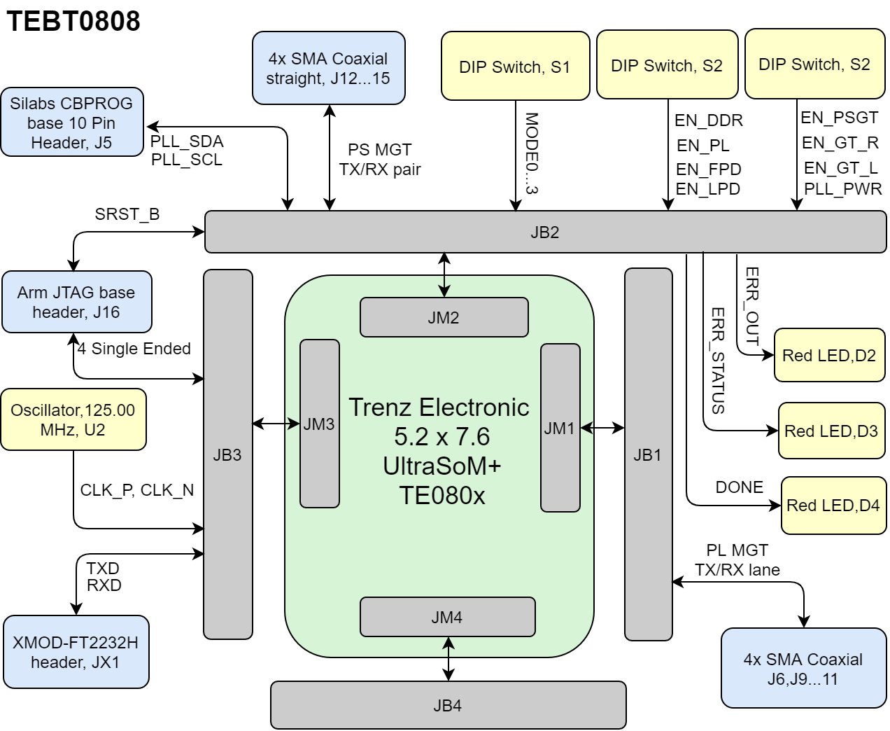
| title | TEBT0808 Block Diagram |
|---|
|
| Scroll Ignore |
|---|
| draw.io Diagram |
|---|
| border | false |
|---|
| viewerToolbar | true |
|---|
| |
|---|
| fitWindow | false |
|---|
| diagramDisplayName | |
|---|
| lbox | true |
|---|
| revision | 21 |
|---|
| diagramName | TEBT0808_OV_BD |
|---|
| simpleViewer | false |
|---|
| width | |
|---|
| links | auto |
|---|
| tbstyle | hidden |
|---|
| diagramWidth | 640 |
|---|
|
| draw.io Diagram |
|---|
| border | false |
|---|
| viewerToolbar | true |
|---|
| |
|---|
| fitWindow | false |
|---|
| diagramDisplayName | |
|---|
| lbox | true |
|---|
| revision | 22 |
|---|
| diagramName | TEBT0808_OV_BD |
|---|
| simpleViewer | false |
|---|
| width | |
|---|
| links | auto |
|---|
| tbstyle | hidden |
|---|
| diagramWidth | 641 |
|---|
|
|
| Scroll Only |
|---|
|
|
Main Components
...
- Uninsulated Power Jack. J7-J8
- SMA Coaxial straight. J6- J9...15
- Surface Mount Schottky Barrier Rectifier. D1
- ARM PJTAG Pin Header J16
- I2C Pin Header, J5
- Board to Board Connectors. J1...4
- MEMS Oscillator, U2
- On-Board LEDs, D2...4
- DIP-Switch, S1...3
- XMOD JTAG Baseheader, JX1
Initial Delivery State
...
| Scroll Title |
|---|
| anchor | Table_SIP_B2B |
|---|
| title | General PL I/O to B2B connectors information |
|---|
|
| Scroll Table Layout |
|---|
| orientation | portrait |
|---|
| sortDirection | ASC |
|---|
| repeatTableHeaders | default |
|---|
| style | |
|---|
| widths | |
|---|
| sortByColumn | 1 |
|---|
| sortEnabled | false |
|---|
| cellHighlighting | true |
|---|
|
| B2B Connector | Interfaces | Number of I/O | Notes |
|---|
J1
| User I/O | 46 Single Ended, 23 Differential 16 Single Ended, 8 Differential 16 Single Ended, 8 Differential 16 Single Ended, 8 Differential 4 Single Ended | IOs are Loop-Back IOs are Loop-Back IOs are Loop-Back IOs are Loop-Back PL_1V8 | J2
| User IO | 28 Single Ended, 14 Differential 6 Single Ended, 3 Differential | IOs are Loop-Back IOs are Loop-Back | | Boot Mode | 4 Single Ended | MODE0...3 | | Control Signals | 25 Single Ended | PLL_SEL0, PLL_SEL1, PLL_RST, EN_GTR, EN_PL, PLL_LOLN, EN_PSGT, ERR_STATUS, ERR_OUT,SRST_B, INIT_B, PROG_B, EN_FPD , EN_LPD , DONE, EN_PLL_PWR, PLL_FINC ,PG_PLL_1V8, LP_GOOD, PG_DDR, PG_PL, PG_FPD, PG_PSGT, PG_GT_R, PG_GT_L | | JTAG Interface | 7 Single Ended | TCK, TDI, TMS, TDO, MR, Rxd, Txd | | I2C | 2 Single Ended | PLL_SCL, PLL_SDA | | Clock | 6 Single Ended, 3 Differential | CLK0, CLK7, CLK8 | J3
| User IO | 24 Single Ended, 12 Differential 24 Single Ended, 12 Differential | Connected to Module FPGA, Bank 48 Connected to Module FPGA, Bank 47 | | Clock | 6 Single Ended, 3 Differential | CLK228, CLK229, CLK230 | | PJTAG Interface | 7 4 Single Ended | PJTAG0_TCK, PJTAG0_TDI, PJTAG0_TMS, PJTAG0_TDO, | | MIO | 45 Single Ended | MIO13..77 | | UART | 2 Single Ended | TXD, RXD | | Power Control Signals | 4 Single Ended | PS_1V8, SI_PLL_1V8, VCCO_48, VCCO_47, PLL_3V3 | | J4 | User I/O | 48 Single Ended, 24 Differential 48 Single Ended, 24 Differential 4 Single Ended 4 Single Ended | IOs are Loopare Loop-Back IOs are Loopare Loop-Back B64_T0...3 B65_T0...3 | | Power pins | 4 Single Ended | VCCO_64, VCCO65 |
|
...
SMA Coaxial Connectors
TEBT0808 is equipped with 8 SMD Coaxial Connectors.
...
JTAG access to the TEBT080X is available through B2B connector JB2 using XMOD JTAG adapter TE0790 adapter.
| Scroll Title |
|---|
| anchor | Table_SIP_JTG |
|---|
| title | JTAG Pins Connection |
|---|
|
| Scroll Table Layout |
|---|
| orientation | portrait |
|---|
| sortDirection | ASC |
|---|
| repeatTableHeaders | default |
|---|
| style | |
|---|
| widths | |
|---|
| sortByColumn | 1 |
|---|
| sortEnabled | false |
|---|
| cellHighlighting | true |
|---|
|
JTAG Signal | B2B Connector | Notes |
|---|
| TMS | J2- 126 |
| | TDI | J2- 122 |
| | TDO | J2- 124 |
| | TCK | J2- 120 |
|
|
There is a DIP switch, S2, on TE0790 adapter The voltages 3.3V (VCC) and VIO (variable SC CPLD I/O-voltage) on TE0790 can be configured by the DIP-switch S2 which must be set as following.
| Scroll Title |
|---|
| anchor | Table_SIP_Xmod_DIP |
|---|
| title | Xmod Adapter DIP-Switch Setting Description |
|---|
|
| Scroll Table Layout |
|---|
| orientation | portrait |
|---|
| sortDirection | ASC |
|---|
| repeatTableHeaders | default |
|---|
| style | |
|---|
| widths | |
|---|
| sortByColumn | 1 |
|---|
| sortEnabled | false |
|---|
| cellHighlighting | true |
|---|
|
| DIP Switch,S2 | Default | Description |
|---|
| 1 | ON | Update Mode JTAG access to SC CPLD only | | 2 | OFF | Must be always in OFF state. | | 3 | OFF | VIO is supplied from Module | | 4 | OFF | 3.3V is supplied by the carrier TEBT0808 |
|
PJTAG
PJTAG access to the TEBT0808 is available through B2B connector JB3.The voltages 3.3V (VCC) and VIO (variable SC CPLD I/O-voltage) can be configured by the DIP-switch S2-3 and S2-4 on TE0790:
| Scroll Title |
|---|
| anchor | Table_SIP_Xmod_DIP |
|---|
| title | Xmod Adapter DIP-Switch Setting Description |
|---|
| | Scroll Table Layout |
|---|
| orientation | portrait |
|---|
| sortDirection | ASC |
|---|
| repeatTableHeaders | default |
|---|
style | widths | | sortByColumn | 1 |
|---|
| sortEnabled | false |
|---|
| cellHighlighting | true |
|---|
| DIP Switch-3 | DIP Switch-4 | 3.3V (VCC) Pin 5 | VIO Pin 6 | Description |
|---|
| OFF | OFF | 3.3V from base | VIO from base | 3.3V (pin 5) and VIO (pin 6) sourced from base |
| OFF | ON | 3.3V from USB | VIO from base | VIO sourced from base by Pin 6 |
| ON | OFF | 3.3V from base | 3.3V from base | VIO and 3.3V source by base (Pin 5 and Pin 6 are shorted and both must be sourced by 3.3V) |
| ON | ON | 3.3V from USB | 3.3V from USB | 3.3V (pin 5) and VIO (pin 6) sourced USB (Pin 5 and Pin 6 are shorted and both are 3.3V) |
PJTAG
PJTAG access to the TEBT0808 is available through B2B connector JB3.
...
| anchor | Table_SIP_JTG |
|---|
| title | PJTAG Pins Connection |
|---|
| JTG | | title | PJTAG Pins Connection |
|---|
|
|
...
JTAG Signal
...
B2B Connector
...
I2C signals can be accessed through pin header J5.
| Scroll Title |
|---|
| anchor | Table_SIP_I2C |
|---|
| title | I2C Connections |
|---|
|
| scroll-tablelayout |
|---|
| orientation | portrait |
|---|
| sortDirection | ASC |
|---|
| repeatTableHeaders | default |
|---|
| style | |
|---|
| widths | |
|---|
| sortByColumn | 1 |
|---|
| sortEnabled | false |
|---|
| cellHighlighting | true |
|---|
|
Signals| Pin Header | Notes | PLL_SCL | J2- 90 | J5- 3 | PLL_SDA | J2- 92 | J5- 7 | |
SMA Coaxial
| Notes |
|---|
| PJTAG_TMS | J3- 94 |
| | PJTAG_TDI | J3- 90 |
| | PJTAG_TDO | J3- 92 |
| | PJTAG_TCK | J3- 88 |
| | PJTAG_SRST | J2- 96 | Connected to SRST_B |
|
The I2C signals can be accessed through pin header J5.
| Scroll Title |
|---|
| anchor | Table_SIP_SMAI2C |
|---|
| title | SMA I2C Connections |
|---|
|
| Scroll Table Layout |
|---|
| orientation | portrait |
|---|
| sortDirection | ASC |
|---|
| repeatTableHeaders | default |
|---|
| style | |
|---|
| widths | |
|---|
| sortByColumn | 1 |
|---|
| sortEnabled | false |
|---|
| cellHighlighting | true |
|---|
|
Designator | Notes | J6 | B230_TX3_P | J1-2 | J9 | B230_RX3_N | J1-5 | | Pin Header | Notes |
|---|
| PLL_SCL | J2- 90 | J5- 3 |
| | PLL_SDA | J2- 92 | J5- 7 |
J10 | B230_RX3_P | J1-3 | J11 | B230_TX3_N | J1-4 | J12 | B505_TX0_N | J2-67 | J13 | B505_TX0_P | J2-69 | J14 | B505_RX0_N | J2-70 | J15 | B505_RX0_P | J2-72
|
Test Points
| Scroll Title |
|---|
| anchor | Table_SIP_TestPoint |
|---|
| title | Test Points Information |
|---|
|
| Scroll Table Layout |
|---|
| orientation | portrait |
|---|
| sortDirection | ASC |
|---|
| repeatTableHeaders | default |
|---|
| style | |
|---|
| widths | |
|---|
| sortByColumn | 1 |
|---|
| sortEnabled | false |
|---|
| cellHighlighting | true |
|---|
|
Test Point | Signals | B2B Connector | Notes |
|---|
| TP 1 | DDR_1V2 | J2-135 |
| | TP 2 | PG_PSGT | J2-82 |
| | TP 3 | ERR_STATUS | J2-86 |
| | TP 4 | PLL_FDEC | J2-94 |
| | TP 5 | EN_LPD | J2-108 |
| | TP 6 | EN_DDR | J2-112 |
| | TP 7 | PG_PL | J2-104 |
| | TP 8 | PG_PLL_1V8 | J2-80 |
| | TP 9 | N_PSGT | J2-84 |
| | TP 10 | ERR_OUT | J2-88 |
| | TP 11 | EN_FPD | J2-102 |
| | TP 12 | LP_GOOD | J2-106 |
| | TP 13 | PG_FPD | J2-110 |
| | TP 14 | PG_DDR | J2-114 |
| | TP 15 | EN_PLL_PWR | J2-77 |
| | TP 16 | PLL_FINC | J2-81 |
| | TP 17 | PG_GT_R | J2-91 |
| | TP 18 | EN_GT_R | J2-95 |
| | TP 19 | EN_PL | J2-101 |
| | TP 20 | EN_GT_L | J2-79 |
| | TP 21 | PLL_SEL0 | J2-93 |
| | TP 22 | PG_GT_L | J2-97 |
| | TP 23 | INIT_B | J2-98 |
| | TP 24 | IN1_P | J2-4 |
| | TP 25 | PLL_SEL1 | J2-87 |
| | TP 26 | PLL_LOLN | J2-85 |
| | TP 27 | PLL_RST | J2-89 |
| | TP 28 | DX_P | J2-119 |
| | TP 29 | DX_N | J2-121 |
| | TP 30 | IN1_N | J2-6 |
| | TP 31 | B505_CLK0_P | J2-10 |
| | TP 32 | B505_CLK0_N | J2-12 |
| | TP 33 | B505_CLK1_P | J2-16 |
| | TP 34 | B505_CLK1_N | J2-18 |
| | TP 35 | B128_CLK1_P | J2-22 |
| | TP 36 | B128_CLK1_N | J2-24 |
| | TP 37 | CLK0_N | J2-1 |
| | TP 38 | CLK0_P | J2-3 |
| | TP 39 | CLK8_P | J2-7 |
| | TP 40 | CLK8_N | J2-9 |
| | TP 41 | CLK7_P | J2-13 |
| | TP 42 | CLK7_N | J2-15 |
| | TP 43 | IN2_P | J3-66 |
| | TP 44 | IN2_N | J3-68 |
| | TP 45 | B230_CLK1_N | J3-59 |
| | TP 46 | B230_CLK1_P | J3-61 |
| | TP 47 | B229_CLK0_N | J3-65 |
| | TP 48 | B229_CLK0_P | J3-67 |
| | TP 49 | PLL_3V3 | J3-152 |
| | TP 50 | GND | J3-155 |
| | TP 51 | PL_1V8 | J1-121 |
| | TP 52 | PS_1V8 | J3-147 |
| | TP 53 | SI_PLL_1V8 | J3-151 |
| | TP 54 | PROG_B | J2-100 |
| | TP 55...56 | GND | - |
|
|
...
| Scroll Title |
|---|
| anchor | Table_OBP |
|---|
| title | On Board Peripherals |
|---|
|
| Scroll Table Layout |
|---|
| orientation | portrait |
|---|
| sortDirection | ASC |
|---|
| repeatTableHeaders | default |
|---|
| style | |
|---|
| widths | |
|---|
| sortByColumn | 1 |
|---|
| sortEnabled | false |
|---|
| cellHighlighting | true |
|---|
|
|
DIP Switch
There are thre three DIP Switches, S1, S2, S3.
...
| Scroll Title |
|---|
| anchor | Table_OBP_DIP |
|---|
| title | DIP Switch S1 |
|---|
|
| Scroll Table Layout |
|---|
| orientation | portrait |
|---|
| sortDirection | ASC |
|---|
| repeatTableHeaders | default |
|---|
| style | |
|---|
| widths | |
|---|
| sortByColumn | 1 |
|---|
| sortEnabled | false |
|---|
| cellHighlighting | true |
|---|
|
S1 switchNotesS1AS1BS1C| S1D |
|
Control signals must be set using DIP Switch S2, S3.
| Scroll Title |
|---|
| anchor | Table_OBP_DIP |
|---|
| title | DIP Switch S2 |
|---|
|
| Scroll Table Layout |
|---|
| orientation | portrait |
|---|
| sortDirection | ASC |
|---|
| repeatTableHeaders | default |
|---|
| style | |
|---|
| widths | |
|---|
| sortByColumn | 1 |
|---|
| sortEnabled | false |
|---|
| cellHighlighting | true |
|---|
|
| DIP Switch S2 | Signals | B2B | S2 switchNotesNotes |
|---|
| S2A | EN_PSGT | J2-84 |
| | S2AS2B | EN_GT_R | J2-95 |
| | S2BS2C | EN_GT_L | J2-97 |
| | S2CS2D | EN_PLL_PWR | J2-77S2D | connected to PG_PL |
|
| Scroll Title |
|---|
| anchor | Table_OBP_DIP |
|---|
| title | DIP Switch S3 |
|---|
|
| Scroll Table Layout |
|---|
| orientation | portrait |
|---|
| sortDirection | ASC |
|---|
| repeatTableHeaders | default |
|---|
| style | |
|---|
| widths | |
|---|
| sortByColumn | 1 |
|---|
| sortEnabled | false |
|---|
| cellHighlighting | true |
|---|
|
| DIP Switch S3 | Signals | B2B | S3 switch | Notes |
|---|
| S3A | EN_DDR | J2-112 | S3A |
| | S3B | EN_LPD | J2-108 | S3B |
| | S3C | EN_PL | J2-101 | S3C |
| | S3D | EN_FPD | J2-102 | S3D |
|
|
LEDs
| Scroll Title |
|---|
| anchor | Table_OBP_LED |
|---|
| title | On-board LEDs |
|---|
|
| Scroll Table Layout |
|---|
| orientation | portrait |
|---|
| sortDirection | ASC |
|---|
| repeatTableHeaders | default |
|---|
| style | |
|---|
| widths | |
|---|
| sortByColumn | 1 |
|---|
| sortEnabled | false |
|---|
| cellHighlighting | true |
|---|
|
| Designator | Color | Connected to | Active Level | Note |
|---|
| D2 | Red | DONE | Active High | Non User LED | | D3 | Red | ERR_STATUS | Active High | Non User LED | | D4 | Red | ERR_OUT | Active High | Non User LED |
|
...
| Scroll Title |
|---|
| anchor | Table_PWR_PC |
|---|
| title | Power Consumption |
|---|
|
| Scroll Table Layout |
|---|
| orientation | portrait |
|---|
| sortDirection | ASC |
|---|
| repeatTableHeaders | default |
|---|
| style | |
|---|
| widths | |
|---|
| sortByColumn | 1 |
|---|
| sortEnabled | false |
|---|
| cellHighlighting | true |
|---|
|
| Power Input Pin | Typical Current |
|---|
| VIN3.3V | TBD* |
|
* TBD - To Be Determined
...