...
| Scroll Title |
|---|
| anchor | Figure_OV_MC |
|---|
| title | TE0821 main components |
|---|
|
| Scroll Ignore |
|---|
| draw.io Diagram |
|---|
| border | false |
|---|
| |
|---|
| diagramName | TE0821_OV_MC |
|---|
| simpleViewer | false |
|---|
| width | |
|---|
| links | auto |
|---|
| tbstyle | hidden |
|---|
| diagramDisplayName | |
|---|
| lbox | true |
|---|
| diagramWidth | 641 |
|---|
| revision | 56 |
|---|
|
|
| Scroll Only |
|---|
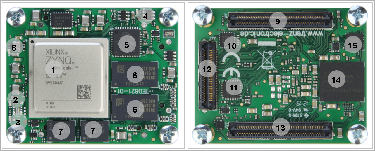 Image Modified Image Modified
|
|
- Xilinx Zynq UltraScale+ XCZU3EG, U1
- Red LED (ERR_OUT), D3
- Green LED (ERR_STATUS), D4
- Red LED (DONE), D1
- GigaBit Ethernet Transceiver10/100/1000 Mbps energy efficient ethernet transceiver, U8
- 8Gb DDR4, U2-U3
- 512 Mb SPI FlashMbit QSPI flash memory, U7-U17
- Board to Board ConnectorB2B connector Samtec Razor Beam, JM1
- Programmable clock generator, U10
- USB2.0 Transceiver, U18
- Board to Board ConnectorB2B connector Samtec Razor Beam, JM3Board to Board Connector
- B2B connector Samtec Razor Beam, JM2
- 8 GByte eMMC , U17memory, U6
- Lattice Semiconductor MachXO2 System Controller CPLD, U21
Initial Delivery State
| Page properties |
|---|
|
Notes : Only components like EEPROM, QSPI flash can be initialized by default at manufacture. If there is no components which might have initial data ( possible on carrier) you must keep the table empty |
...
| Scroll Title |
|---|
| anchor | Table_OV_IDS |
|---|
| title | Initial delivery state of programmable devices on the module |
|---|
|
| Scroll Table Layout |
|---|
| orientation | portrait |
|---|
| sortDirection | ASC |
|---|
| repeatTableHeaders | default |
|---|
| style | |
|---|
| widths | |
|---|
| sortByColumn | 1 |
|---|
| sortEnabled | false |
|---|
| cellHighlighting | true |
|---|
|
Storage device name | Content | Notes |
|---|
SPI QSPI Flash OTP AreaMemory | Not programmed | Except serial number programmed by flash vendor. | SPI Flash Quad Enable bit | Programmed | - | SPI Flash main array | Not programmed | - | eFUSE USER | Not programmed | - | eFUSE Security | Not programmed | - |
| eMMC Memory | Not programmed |
| | Programmable Clock GeneratorSi5338 OTP NVM | Not programmed | - |
| | CPLD (LCMXO2-256HC) | SC0820-02 QSPI FirmwareSee Boot Process section. |
|
|
Configuration Signals
| Page properties |
|---|
|
- Overview of Boot Mode, Reset, Enables.
|
...
| Scroll Title |
|---|
| anchor | Table_OV_RST |
|---|
| title | Reset process. |
|---|
|
| Scroll Table Layout |
|---|
| orientation | portrait |
|---|
| sortDirection | ASC |
|---|
| repeatTableHeaders | default |
|---|
| style | |
|---|
| widths | |
|---|
| sortByColumn | 1 |
|---|
| sortEnabled | false |
|---|
| cellHighlighting | true |
|---|
|
Signal | B2B | I/O | Note |
|---|
EN | JM1-28 | Input | CPLD Enable Pin |
|
Signals, Interfaces and Pins
...
| Scroll Title |
|---|
| anchor | Table_SIP_B2B |
|---|
| title | General PL I/O to B2B connectors information |
|---|
|
| Scroll Table Layout |
|---|
| orientation | portrait |
|---|
| sortDirection | ASC |
|---|
| repeatTableHeaders | default |
|---|
| style | |
|---|
| widths | |
|---|
| sortByColumn | 1 |
|---|
| sortEnabled | false |
|---|
| cellHighlighting | true |
|---|
|
| FPGA Bank | Type | B2B Connector | I/O Signal Count |
|---|
I/O Signal Count | 64HP48 | User| 24x I/O, 12x LVDS Pairs | Variable | Max voltage 3.3V | | 25 | HD | JM1 | 24x I/O, 12x LVDS Pairs | Variable | Max voltage 3.3V | | 26 | HD | JM1 | 24x I/O, 12x LVDS Pairs | Variable | Max voltage |
18V64HP2 | | 24x I/O, 12x LVDS Pairs | Variable |
User 18V18 | 18x I/O, 9x LVDS Pairs | Variable |
User16 | 16x I/O, 8x LVDS Pairs | Variable |
User | Max voltage 1.8V | 66 | HP | JM1 | 48 |
User500MIOJM1 | 8 | 1.8V | - | | JM3 | 16x I/O, 8x LVDS Pairs | - | 4x lanes |
501 | MIO | JM1 | 6 | 3.3V | -4 lanes-505GTR CLK | JM3 | 1 differential input | - | -
|
JTAG Interface
JTAG access to the TExxxx SoM through B2B connector JMX.
...