Figure 1: Module TE0717 with Carrier TEB0717
1 Overview
This guide showcases the important components of the module-carrier combination TE0717 + TEB0717 and introduces the available script-based reference design to get the board up and running.
1.1 Prerequisites
| Hardware | Software |
|---|---|
|
|
1.2 Getting Started with the TE0717
The module TE0717 has a Xilinx Spartan-7 FPGA onboard that allows you to create extensive digital hardware and software designs.
Most of the FPGA IOs are spread arround the carrier. The TE0717 is assembled with HyperRAM(64 Mbit), QSPI non-volatile Flash memory(64 Mbit) and plenty of IOs which enable great hardware expandability. For communication and configuration the carrier offers a JTAG/UART Interface.
This Getting Started Guide shows how to set up the board, attach the jumpers, wire it up and connect it with the software. Over the course of this guide we will go into "how to use the provided reference design" and touch several aspects of "how to modify the design according to your needs". This includes changing the Vivado Block Design, regenerating the bitstream and using the hardware export(.xsa file) in Vitis to develop software that runs on the MicroBlaze. Here we will not build the whole project from scratch since that would go beyond the scope of this guide.
1.3 Official Documentation
- Official links to the shop:
- coming soon!
- coming soon!
- Technical Reference Manual:
- coming soon!
- Resources & Reference Designs:
1.4 TE0717 module + TEB0717 carrier - Hardware Features
- FPGA
- Xilinx Spartan-7 - XC7S25-1FTGB196C
- Clocking
- 100 MHz clock from clocking chip SiT8008 on TE0717 module
- Memory
- 8 MByte DDR HyperRAM
- 8 MByte Quad-SPI Flash
- Communication
- On carrier USB-JTAG Programming
- Connectors
- B2B connector - Module(JM1) to Carrier(JB1)
- Unpopulated PIN Header on carrier(J3, J4, J5)
- Configuration and Debug
- On carrier USB-JTAG interface
- Jumper
- Adjustable BANK34 supply voltage (J2)
- Power source (J1)
- General Purpose I/O
- 2x2 user LEDs (red,green)
Firgure 2: TE0717+TEB0717 Hardware Blockdiagram
Basic IOs<->FPGA connections are as following, Table 1:
| Color | Signal | FPGA Pin | Function | |
|---|---|---|---|---|
| LED D1(on carrier) | red | B14_L24_P | P10 | general purpose |
| LED D2(on carrier) | green | B14_L24_N | P11 | " |
| LED D1(on module) | red | LED1 | D14 | " |
| LED D2(on module) | green | LED2 | C14 | " |
| Clock | -- | CLK_100M | G11 | singled ended 100MHz clock |
Information on IO routing and FPGA pin connections can be found in the schematics.
2 Board Power-Up
2.1 TE0717 Hardware Setup and Power up
- Before connecting the Board to the PC, make sure to properly mount the module TE0717 onto the carrier TEB0717 via the B2B connector like in Figure 1.
Check the Jumper setting
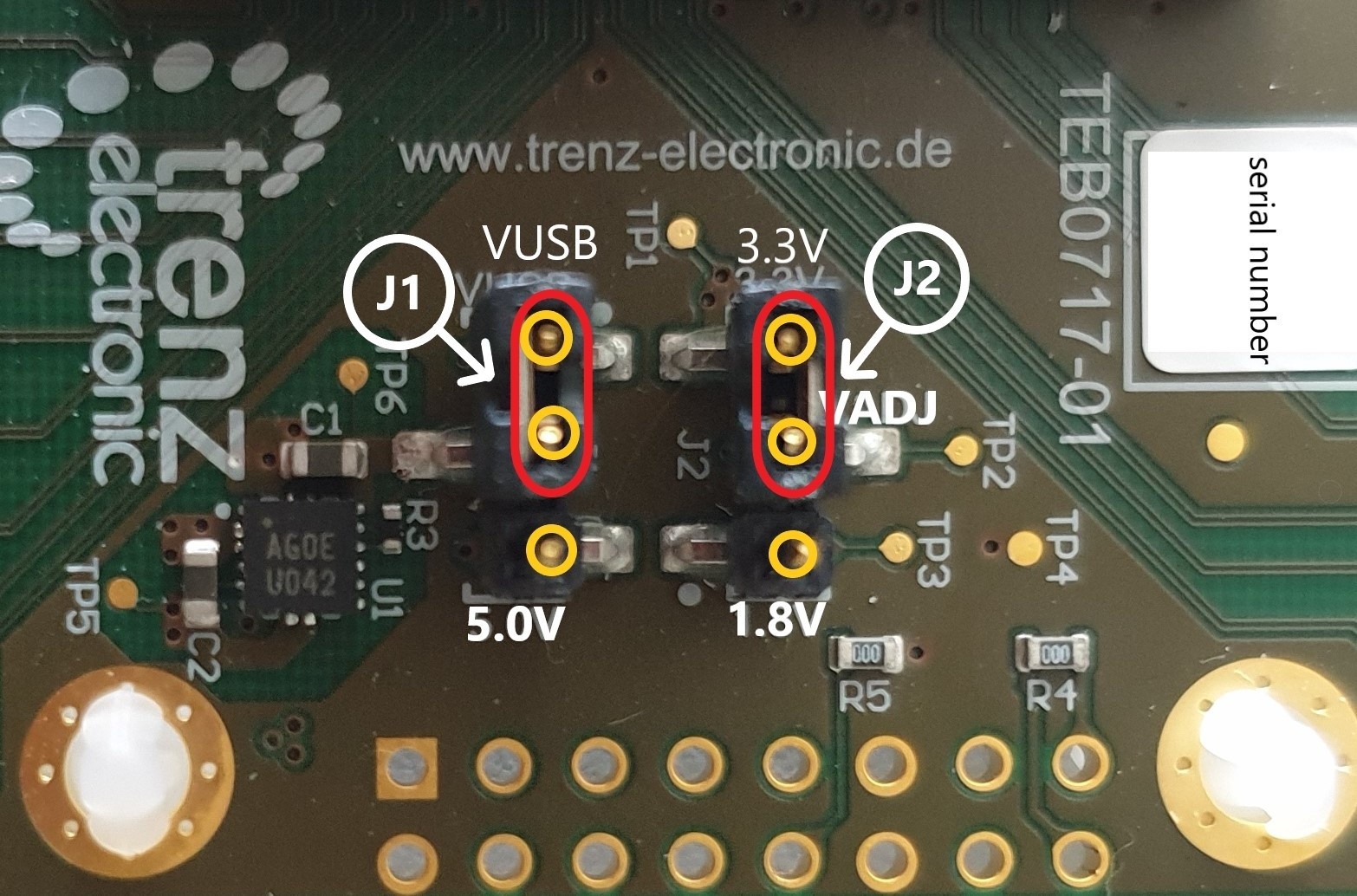
Figure 3: Jumper settingThe Voltage set with Jumper J1 determines the source of the input voltage for the voltages regulator chip U1 to the left of J1. Either 5V from the MicroUSB port(VUSB) or 5V from pin header J4.
With the shown setting of Jumper J2 the voltage VADJ is set to 3.3V that comes from the carriers voltage regulator chip U1. The 1.8V comes from the module. The Voltage VADJ is wired to the module and is used as the BANK34 supply voltage.
- Use a MicroUSB cable to connect your board to the PC.cc
All the LEDs are simply routed to the FPGA, hence none of them should be turned on. If the qspi flash on the module is preloaded with a design though, it might be that some LEDs are blinking.
In case the QSPI Flash is loaded with the reference design, you can connect to the board with a program like PuTTY. Just open up a serial session with baud-rate of 9600 and the right COM-port(visible in Device Manager).
You may need to press the RESET-button.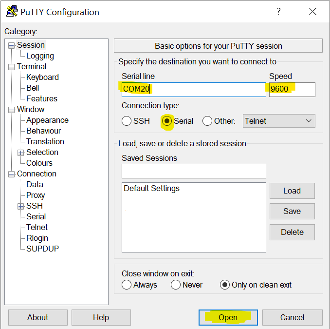
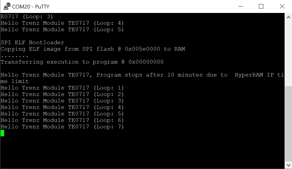
Figure 4: Terminal(MicroBlaze output)
2.2 Reference Design - Description
We provide a reference design that interacts with most of the peripheral on the module. The provided design "TE0717 test board" shows how to connect the different parts of the module to simplify the development of your own application. You can use it for your own design but keep in mind the overall FPGA resources and power consumption before deployment.
The reference design we use in this guide is "TE0717 test board". The most important steps to get it up and running are explained on TE0717 Test Board. The Download is available here.
The reference design is only usable with the specified Vivado/Vitis version. Do never use different Versions of Xilinx Software for the same Project. (please only use reference design 2021.2 with vitis installation 2021.2)
The components of the reference design are illustrated in the following figure:
Figure 5: Blockdiagram of the Reference Design
The Cores are connected via the AXI Interface with the MicroBlaze Processor. How they are mapped into the address space can be seen in the address editor:
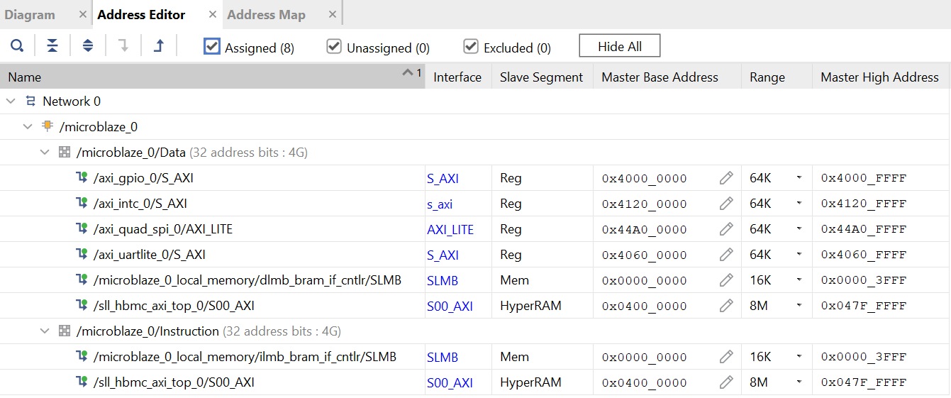
Figure 6: Vivado Address Editor - Address Mapping
For example the AXI GPIO IP which has a LED1 connected to it, can be controlled with software by raising the bits mapped to the address 0x4000 0000.
The VIO Core enables you to control connected IOs via the Vivado Hardware Manager(like LED2).
2.3 Design Flow
The following Vivado Blockdiagram illustrates the different parts of the reference design and what ports are connected outside the FPGA.

Block Design
Figure 7: Blockdesign of the provided reference design
2.3.1 Add IP to the Design
In this section we are going to add a AXI GPIO IP to the Blockdesign and connect the Carrier LEDs to the IP. After generating the Bitstream we export the design to Vitis and control the LEDs with software running on the MicroBlaze.
Necessary steps:
- First open the prebuilt reference design with the "_create_win_setup.cmd" script and open the block design.
Add a second "AXI GPIO IP" from the IP catalog to the block design.

Figure 8: Adding AXI GPIO IP
- Configure the IP by double-clicking on the IP. Make the changes according to figure 9 and click "ok".

Figure 9: AXI GPIO Configuration
Right click on the port and choose "Make external" in the context menu

Figure 10: Make the AXI GPIO Ports external for the Carrier LEDs
- Next step is to run the connection automation

Figure 11: Run Connection Automation
- Now the address mapping in the address editor should be set like:

Figure 12: Address Editor - AXI GPIO 1
Next, the constraints for the two leds have to be set. Just copy the constraints from the other two onboard LEDs in the "_i_io.xdc" and apply the changes:

Figure 13: on carrier LEDs constraintsNow you are all set in Vivado and you can build the bitstream + export the project to Vitis with the following command in the TCL-console:

Figure 14: Build bitstream and export project
After that was successful you can test the functionality of the VIO Core by programming the FPGA and controlling the onBoard LED2:

Figure 15: Program FPGA and control onboard LED through the VIO IP Core.If that works correctly you can build the Vitis project with the provided C-Applications with the following command:

Figure 16: Build Vitis project with built vivado design
- In Vitis open the hello_te0717 application:


Figure 17: Vitis hello_te0717
- Add the following lines of code to also make both of the carrier LEDs blink:

Figure 18: hello_te0717 adding code for controlling carrier LEDs'
- Save and Build project
Right-Click on the application and choose "Run Configuration"

Figure 19: Run Configuration
Since we already programmed the FPGA, uncheck the following:

Figure 20: Run Configuration - Uncheck
- Click on Apply and Run to execute the program on the MicroBlaze. You Should now see the LEDs of the module and carrier blinking in sequence.
Also if you open up a serial connection to the board with a program like PuTTY, you should see output like described in section 2.1
3 Notes
Document Revision History
Table of contents
Overview
Content Tools