Overview
The Trenz Electronic TEP0001 is an industrial-grade dual CAN FD transceiver with Pmod interface.
Features
- Digilent Pmod interface compatible
- Dual CAN FD PHY's
- Texas Instruments TCAN337G
- Up to 5Mbit data rate
- Compatible with ISO 11898-2
- Bus pin fault protection of ±14 V
Integrated 12 kV IEC-61000-4-2 ESD contact discharge protection
- 10 pin headers (IDC cable to DB9)
- One CAN FD transceiver has extra 3-pin screw connector terminal
- Single 3.3V supply
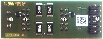
Main Components
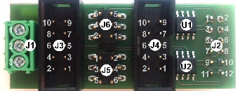
J1. Screw connector terminal of CAN0 bus
J2. 2.54mm pitch 2x6-pin header Pmod interface
J3. 2.54mm pitch 2x5-pin box header, CAN0 bus
J4. 2.54mm pitch 2x5-pin box header, CAN1 bus
J5. 2.54mm pitch SMT 2x3-pin jumper block, can also be used as CAN1 bus connector
J6. 2.54mm pitch SMT 2x3-pin jumper block, can also be used as CAN0 bus connector
U1. Texas Instruments TCAN337G CAN FD transceiver, CAN0
U2. Texas Instruments TCAN337G CAN FD transceiver, CAN1
Interfaces and Pins
J1 Connector
| Pin | Signal | Notes |
|---|---|---|
| 1 | CAN0_P | U1 high level CAN bus line |
| 2 | GND | U1 ground connection |
| 3 | CAN0_N | U1 low level CAN bus line |
J2 Connector
| Pin | Signal | Notes | Pin | Signal | Notes | |
|---|---|---|---|---|---|---|
| 1 | CAN0_TX | U1 CAN transmit data input, integrated pull up | 2 | CAN1_TX | U2 CAN transmit data input, integrated pull up | |
| 3 | CAN0_RX | U1 CAN receive data output, tri-state | 4 | CAN1_RX | U2 CAN receive data output, tri-state | |
| 5 | CAN0_S | U1 silent mode, integrated pull down | 6 | CAN1_S | U2 silent mode, integrated pull down | |
| 7 | CAN0_F | U1 open drain fault output | 8 | CAN1_F | U2 open drain fault output | |
| 9 | GND | U1 ground connection | 10 | GND | U2 ground connection | |
| 11 | 3.3V | U1 3.3-V supply voltage | 12 | 3.3V | U2 3.3-V supply voltage |
J3 Connector
| Pin | Signal | Notes | Pin | Signal | Notes | |
|---|---|---|---|---|---|---|
| 1 | N/A | - | 2 | GND | U1 ground connection | |
| 3 | CAN0_N | U1 low level CAN bus line | 4 | CAN0_P | U1 high level CAN bus line | |
| 5 | GND | U1 ground connection | 6 | N/A | - | |
| 7 | N/A | - | 8 | N/A | - | |
| 9 | N/A | - | 10 | N/A | - |
J4 Connector
| Pin | Signal | Notes | Pin | Signal | Notes | |
|---|---|---|---|---|---|---|
| 1 | N/A | - | 2 | GND | U2 ground connection | |
| 3 | CAN1_N | U2 low level CAN bus line | 4 | CAN1_P | U2 high level CAN bus line | |
| 5 | GND | U2 ground connection | 6 | N/A | - | |
| 7 | N/A | - | 8 | N/A | - | |
| 9 | N/A | - | 10 | N/A | - |
J5 Jumper Block/Connector
Place jumpers on pins 1-3 and 2-4 to activate on-board CAN bus terminator of U2. J5 header can also be used as CAN bus connector, refer to table below for pin mapping.
| Pin | Signal | Note | Pin | Signal | Note | |
|---|---|---|---|---|---|---|
| 3 | CAN1_N | U2 low level CAN bus line | 4 | CAN1_P | U2 high level CAN bus line | |
| 5 | GND | U2 ground connection | 6 | GND | U2 ground connection |
J6 Jumper Block/Connector
Place jumpers on pins 1-3 and 2-4 to activate on-board CAN bus terminator of U2. J5 header can also be used as CAN bus connector, refer to table below for pin mapping.
| Pin | Signal | Note | Pin | Signal | Note | |
|---|---|---|---|---|---|---|
| 3 | CAN0_N | U1 low level CAN bus line | 4 | CAN0_P | U1 high level CAN bus line | |
| 5 | GND | U1 ground connection | 6 | GND | U1 ground connection |
Operating Conditions, Ratings and Dimensions
Recommended Operating Conditions
| Minimum | Maximum | Unit | |
|---|---|---|---|
| Supply voltage | 3 | 3.6 | V |
| Operational free-air temperature | -40 | 125 | °C |
Absolute Maximum Ratings
| Parameter | Minimum | Maximum | Unit |
|---|---|---|---|
| Supply voltage range | -0.3 | 5 | V |
| Voltage at any bus terminal (CANH or CANL) | -14 | 14 | V |
| Operating temperature range | -40 | 150 | °C |
| Storage temperature | - | 150 | °C |
Refer to Texas Instruments TCAN337G product datasheet for additional information about conditions and ratings.
Power Requirements
3.3V supply voltage TBD* (180 mA max per one CAN FD transceiver in "Normal Mode", dominant state with bus fault as per TCAN337G datasheet).
* TBD - To Be Determined soon with reference design setup.
Physical Dimensions
Module size: 54 mm × 20.5 mm.
Mating height of the J8 connector from the PCB: 8mm
PCB thickness: 1.6mm
Highest part on PCB J1, J2 and J5 connectors, approximately 9.5mm from the PCB.
Document Change History
Date | Rrevision | Contributors | Description |
|---|---|---|---|
| 05.09.2016 | Initial document. |
Hardware Revision History
| Date | Revision | Notes | PCN |
|---|---|---|---|
| 22.08.2016 | 01 | Initial batch | - |
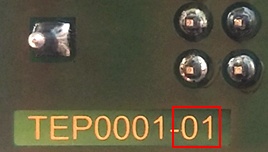
Hardware revision number is printed on the PCB board next to the module model number separated by the dash.
Disclaimer
Unable to render {include} The included page could not be found.
Overview
Content Tools