Overview
The Trenz Electronic TEP0001 is an industrial-grade dual CAN FD transceiver with Pmod interface.
Features
- Digilent Pmod interface compatible
- Dual CAN FD PHY's (CAN0 and CAN1)
- Texas Instruments TCAN337G
- Up to 5Mbit data rate
- Compatible with ISO 11898-2
- Bus pin fault protection of ±14 V
Integrated 12 kV IEC-61000-4-2 ESD contact discharge protection
- 10 pin headers (IDC cable to DB9)
- One CAN FD transceiver has extra 3-pin screw connector terminal
- Single 3.3V supply
Main Components
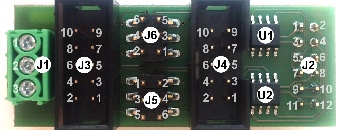
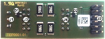
J1. Screw connector terminal of CAN0 bus
J2. 2.54mm pitch 2x6-pin header Pmod interface
J3. 2.54mm pitch 2x5-pin box header, CAN0 bus
J4. 2.54mm pitch 2x5-pin box header, CAN1 bus
J5. 2.54mm pitch SMT 2x3-pin jumper block, can also be used as CAN1 bus connector
J6. 2.54mm pitch SMT 2x3-pin jumper block, can also be used as CAN0 bus connector
U1. Texas Instruments TCAN337G CAN FD transceiver, CAN0
D1. Bourns CDSOT23-T24CAN CANbus Protector, CAN0
U2. Texas Instruments TCAN337G CAN FD transceiver, CAN1
D2. Bourns CDSOT23-T24CAN CANbus Protector, CAN1
REV 01 PCB's have the PMOD connector mounted for Right Angle connection to PMOD Baseboard.
Interfaces and Pins
J1 Connector, CAN0 Bus
| Pin | Signal | Notes |
|---|---|---|
| 1 | CAN0_P | U1 high level CAN bus line |
| 2 | GND | U1 ground connection |
| 3 | CAN0_N | U1 low level CAN bus line |
J2 Connector, Pmod Interface
| Pin | Signal | Notes | Pin | Signal | Notes | |
|---|---|---|---|---|---|---|
| 1 | CAN0_TX | U1 CAN0 transmit data input, integrated pull up | 2 | CAN1_TX | U2 CAN1 transmit data input, integrated pull up | |
| 3 | CAN0_RX | U1 CAN0 receive data output, tri-state | 4 | CAN1_RX | U2 CAN1 receive data output, tri-state | |
| 5 | CAN0_S | U1 silent mode,integrated pull down | 6 | CAN1_S | U2 silent mode, integrated pull down | |
| 7 | CAN0_F | U1 open drain fault output | 8 | CAN1_F | U2 open drain fault output | |
| 9 | GND | U1 ground connection | 10 | GND | U2 ground connection | |
| 11 | 3.3V | U1 3.3V supply voltage | 12 | 3.3V | U2 3.3V supply voltage |
J3 Connector, CAN0 Bus
| Pin | Signal | Notes | Pin | Signal | Notes | |
|---|---|---|---|---|---|---|
| 1 | N/A | - | 2 | GND | U1 ground connection | |
| 3 | CAN0_N | U1 low level CAN bus line | 4 | CAN0_P | U1 high level CAN bus line | |
| 5 | GND | U1 ground connection | 6 | N/A | - | |
| 7 | N/A | - | 8 | N/A | - | |
| 9 | N/A | - | 10 | N/A | - |
J4 Connector, CAN1 Bus
| Pin | Signal | Notes | Pin | Signal | Notes | |
|---|---|---|---|---|---|---|
| 1 | N/A | - | 2 | GND | U2 ground connection | |
| 3 | CAN1_N | U2 low level CAN bus line | 4 | CAN1_P | U2 high level CAN bus line | |
| 5 | GND | U2 ground connection | 6 | N/A | - | |
| 7 | N/A | - | 8 | N/A | - | |
| 9 | N/A | - | 10 | N/A | - |
J5 Jumper Block/Connector CAN1 bus
Close pins 1-3 and 2-4 with jumpers to enable on-board terminator for CAN1 bus. J5 header can also be used as CAN1 bus connector, refer to table below for pin mapping.
| Pin | Signal | Note | Pin | Signal | Note | |
|---|---|---|---|---|---|---|
| 3 | CAN1_N | U2 low level CAN bus line | 4 | CAN1_P | U2 high level CAN bus line | |
| 5 | GND | U2 ground connection | 6 | GND | U2 ground connection |
J6 Jumper Block/Connector, CAN0 bus
Close pins 1-3 and 2-4 with jumpers to enable on-board terminator for CAN0 bus. J6 header can also be used as CAN0 bus connector, refer to table below for pin mapping.
| Pin | Signal | Note | Pin | Signal | Note | |
|---|---|---|---|---|---|---|
| 3 | CAN0_N | U1 low level CAN bus line | 4 | CAN0_P | U1 high level CAN bus line | |
| 5 | GND | U1 ground connection | 6 | GND | U1 ground connection |
Operating Conditions, Ratings and Dimensions
Recommended Operating Conditions
| Minimum | Maximum | Unit | |
|---|---|---|---|
| Supply voltage | 3 | 3.6 | V |
| Operational free-air temperature | -40 | 125 | °C |
Absolute Maximum Ratings
| Parameter | Minimum | Maximum | Unit |
|---|---|---|---|
| Supply voltage range | -0.3 | 5 | V |
| Voltage at any bus terminal (CANH or CANL) | -14 | 14 | V |
| Operating temperature range | -40 | 150 | °C |
| Storage temperature | - | 150 | °C |
Refer to Texas Instruments TCAN337G product datasheet for additional information about conditions and ratings.
Power Requirements
3.3V supply voltage TBD* (180 mA max per one CAN FD transceiver in "Normal Mode", dominant state with bus fault as per TCAN337G datasheet).
* TBD - To Be Determined soon with reference design setup.
Physical Dimensions
Module size: 54 mm × 20.5 mm.
Mating height of the J2 connector from the PCB: 8mm
PCB thickness: 1.6mm
Highest parts on PCB are J1, J3 and J4 connectors, approximately 9.5mm from the PCB.
Document Change History
Date | Rrevision | Contributors | Description |
|---|---|---|---|
| 05.09.2016 | Initial document. |
Hardware Revision History
| Date | Revision | Notes | PCN |
|---|---|---|---|
| 22.08.2016 | 01 | Initial batch | - |
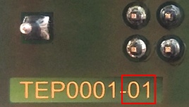
Hardware revision number is printed on the PCB board next to the module model number separated by the dash.
Disclaimer
Unable to render {include} The included page could not be found.
Overview
Content Tools