The Xilinx FPGA itself on the Trenz Electronic USB FX2 modules is blank when powered off. To define an FPGA functionality, a logic architecture should be defined and loaded into the device at power-on.
The reference design architecture was built using Xilinx Embedded Development Kit (EDK). Basically, it is an embedded system on a chip with a Xilinx MicroBlaze 32-bit soft microprocessor. The MicroBlaze i(MB) nitializes and sets up the system.
Standard EDK cores are used to implement a serial interface (XPS_UARTLITE), an SPI FLASH interface (XPS_SPI), a timer / counter block (XPS_TIMER) and an interrupt controller (XPS_INTC).
Besides standard IP cores, the reference architecture contains three custom IP cores:
- XPS_I2C_SLAVE: forwards commands coming from the USB bus towards the MicroBlaze;
- XPS_NPI_DMA: custom DMA between DDR SDRAM and other multiple sources;
- XPS_FX2: used for high speed bidirectional communication between the FPGA and a host PC.
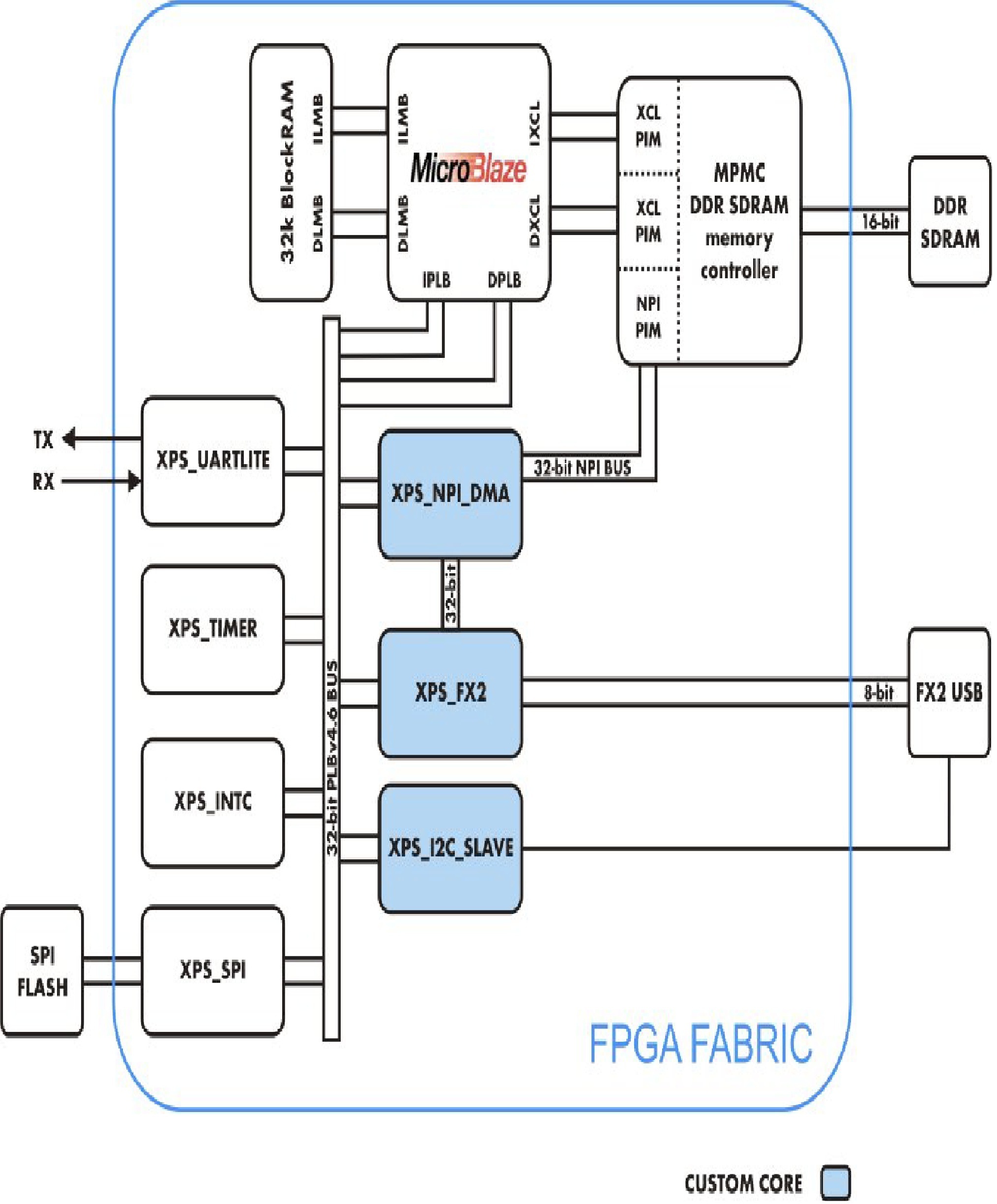
XPS_I2C_SLAVE
It is a logic block for low speed bidirectional communication between the FPGA and a host PC. It is usually used for command, settings and status communication. It contains 6 × 32-bit memory mapped registers:
- 3 for host => FPGA communication (FX22MB registers)
- 3 for FPGA => host communication (MB2FX2 registers)
When the host sends commands to the MicroBlaze (MB) soft embedded processor, an interrupt is triggered. When the MB writes data to MB2FX2_reg0, the interrupt (INT0) is sent to the Cypress EZ-USB FX2LP USB microcontroller. When the FX2 microcontroller receives an interrupt, it reads all MB2FX2 registers.
XPS_NPI_DMA
It is a high speed DMA (direct memory access) engine which connects to the MPMC (Multi-Port Memory Controller) VFBC (Video Frame Buffer Controller) port. It enables high speed data streaming to/from external memory (DDR SDRAM) and multiple sources. It can be controlled by a processor using 6 × 32-bit memory mapped registers attached to the PLB (peripheral local bus). For more information about registers, see Xilinx LogiCORE IP Multi-Port Memory Controller (MPMC) data sheets (Xilinx DS643), Video Frame Buffer Controller PIM section.
When data is sent from the USB-host to a USB FX2 module high-speed endpoint (high speed communication channel), it is automatically stored into the RAM by the custom built DMA engine (XPS_NPI_DMA) at a specified buffer location. The reference design software running on the MicroBlaze verifies the transferred data at the end of transmission and sends to the USB host a notification about the data test (passed / failed).
XPS_FX2
It is a logic block for high speed bidirectional communication between the FPGA and a host PC. It contains 2 kbyte FIFOs for data buffering. More information about the 5 × 32-bit memory mapped registers is contained in the #project_root#/pcores/xps_fx2_v1_00_a/doc/ folder of the reference design project folder.
When data is sent form a USB FX2 module high-speed endpoint to the USB host, it is automatically fetched from the RAM via the custom DMA engine (XPS_NPI_DMA)and forwarded to the XPS_FX2 core in 1-kbyte packets. MicroBlaze throttles the throughput to prevent XPS_FX2 TX FIFO overflow.
Overview
Content Tools