Table of Contents
Overview
The Trenz Electronic TE0841-01 is an industrial-grade 4 x 5 cm SoM integrating Xilinx Kintex UltraScale FPGA, 1 GByte of DDR4 SDRAM, 32 MByte QSPI Flash for configuration and operation, and powerful switch-mode power supplies for all on-board voltages. Numerous configurable I/Os are provided via rugged high-speed strips. All this on a tiny footprint, smaller than a credit card size at very competitive price. All Trenz Electronic 4 x 5 cm SoMs are mechanically compatible.
Key Features
- Xilinx Kintex UltraScale FPGA (XCKU035 or XCKU040)
- 2 banks of 512 MByte, 16 bit wide DDR4 SDRAM
- 256 Mbit (32 MByte) QSPI Flash
- 3 x Samtec Razor Beam LSHM B2B, 260 terminals total
- User I/O: 60 x HR, 84 x HP
- Serial transceiver: 8 x GTH lanes (TX/RX)
- GT clock inputs: 2 - Clocking
- Si5338 - 4 output PLLs, GT and PL clocks
- 200 MHz LVDS oscillator - All power supplies on-board, single power source operation
- Evenly spread supply pins for optimized signal integrity
- Size: 40 x 50 mm
- 3 mm mounting holes for skyline heat spreader
- Rugged for industrial applications
Additional assembly options for cost or performance optimization plus high volume prices are available on request.
Block Diagram
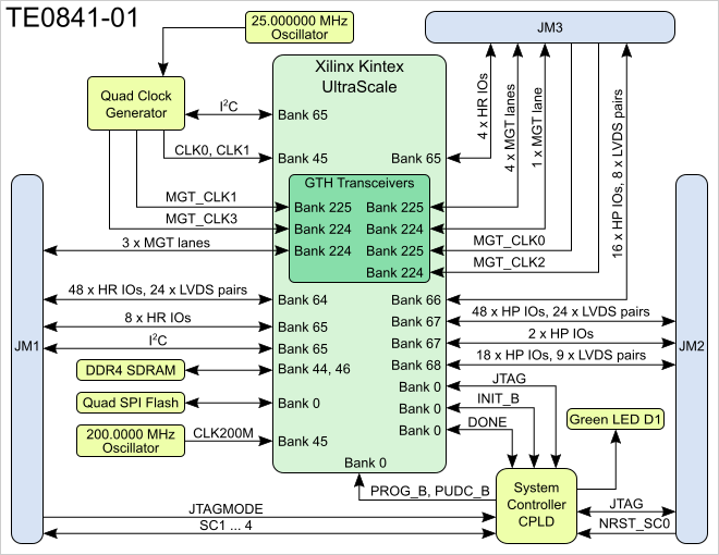
Figure 1: TE0841-01 block diagram.
Main Components
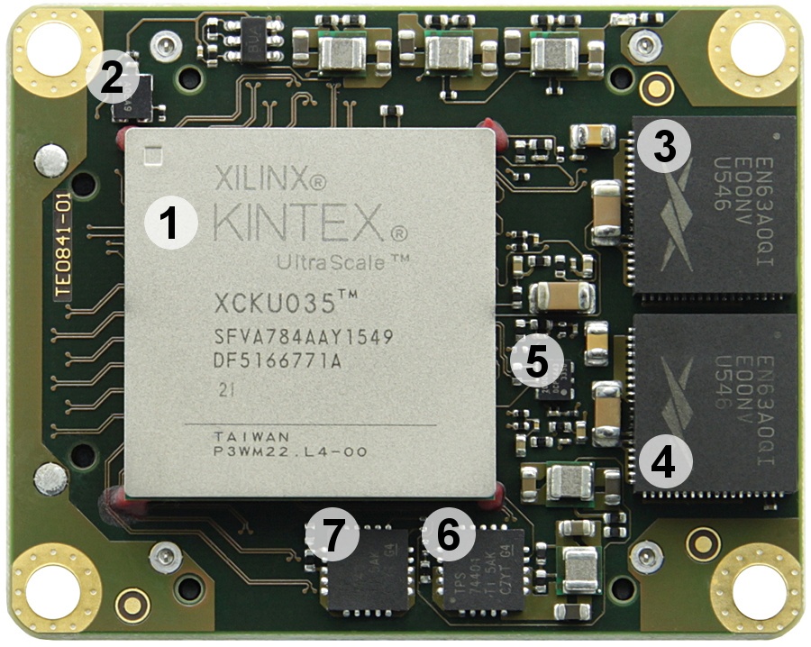
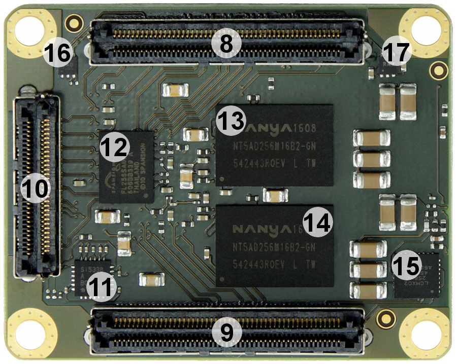
Figure 2: TE0841-01 main components.
- Xilinx Kintex UltraScale FPGA, U1
- Ultra performance oscillator @25.000000 MHz, U3
- 12A PowerSoC DC-DC converter (0.95V), U14
- 12A PowerSoC DC-DC converter (0.95V), U7
- Low-jitter precision LVDS oscillator @200.0000 MHz, U11
- Low-dropout (LDO) linear regulator (MGTAVTT 1.20V), U8
- Low-dropout (LDO) linear regulator (MGTAVCC 1.02V), U12
- Samtec Razor Beam™ LSHM-150 B2B connector, JM1
- Samtec Razor Beam™ LSHM-150 B2B connector, JM2
- Samtec Razor Beam™ LSHM-130 B2B connector, JM3
- Programmable quad clock generator, U2
- 32 MByte QSPI Flash, U6
- 4 Gbit DDR4 SDRAM, U4
- 4 Gbit DDR4 SDRAM, U5
- System Controller CPLD, U18
- Low-dropout (LDO) linear regulator (MGTAUX), U9
- Ultra-low power low-dropout (LDO) regulator (VBATT), U19
Initial Delivery State
Storage device name | Content | Notes |
|---|---|---|
OTP Flash area | Empty | Not programmed. |
| Quad clock generator |
Table 1: TE0841-01 module initial delivery state of programmable on-board devices.
Signals, Interfaces and Pins
Board to Board (B2B) I/Os
Table below lists bank number, bank type, B2B connection, I/O signal/LVDS pair count and power source for each FPGA PL I/O bank connected to the B2B connectors:
| FPGA Bank | Type | B2B Connector | I/O Signal Count | Voltage | Notes |
|---|---|---|---|---|---|
| 64 | HR | JM1 | 48 IOs, 24 LVDS pairs | B64_VCCO | B64_VCCO supplied by the carrier board. |
| 65 | HR | JM1 | 8 IOs | 3.3V | Powered by on-module power supply. |
| 65 | HR | JM3 | 4 IOs, 2 LVDS pairs | 3.3V | Powered by on-module power supply. |
| 66 | HP | JM3 | 16 IOs, 8 LVDS pairs | B66_VCCO | B66_VCCO supplied by the carrier board |
| 67 | HP | JM2 | 48 IOs, 24 LVDS pairs | B67_VCCO | B67_VCCO supplied by the carrier board |
| 67 | HP | JM2 | 2 IOs | B67_VCCO | B67_VCCO supplied by the carrier board |
| 68 | HP | JM2 | 18 IOs, 9 LVDS pairs | B68_VCCO | B68_VCCO supplied by the carrier board |
Table 2: General overview of FPGA's PL I/O signals connected to the B2B connectors.
For detailed information about the pin out, please refer to the Pin-out Tables.
MGT Lanes
MGT (Multi Gigabit Transceiver) lane consists of one transmit and one receive (TX/RX) differential pairs, two signals each or four signals total per one MGT lane. Following table lists lane number, MGT bank number, transceiver type, signal schematic name, board-to-board pin connection and FPGA pins connection:
| Lane | Bank | Type | Signal Name | B2B Pin | FPGA Pin |
|---|---|---|---|---|---|
| 0 | 225 | GTH |
|
|
|
| 1 | 225 | GTH |
|
|
|
| 2 | 225 | GTH |
|
|
|
| 3 | 225 | GTH |
|
|
|
| 4 | 224 | GTH |
|
|
|
| 5 | 224 | GTH |
|
|
|
| 6 | 224 | GTH |
|
|
|
| 7 | 224 | GTH |
|
|
|
Table 3: MGT lanes
Below are listed MGT banks reference clock sources.
| Clock signal | Bank | Source | FPGA Pin | Notes |
|---|---|---|---|---|
| MGT_CLK0_P | 225 | B2B, JM3-33 | MGTREFCLK0P_225, Y6 | Supplied by the carrier board. |
| MGT_CLK0_N | 225 | B2B, JM3-31 | MGTREFCLK0N_225, Y5 | Supplied by the carrier board. |
| MGT_CLK1_P | 225 | U2, CLK1B | MGTREFCLK1P_225, V6 | On-board Si5338A. |
| MGT_CLK1_N | 225 | U2, CLK1A | MGTREFCLK1N_225, V5 | On-board Si5338A. |
| MGT_CLK2_P | 224 | B2B, JM3-34 | MGTREFCLK2P_224, AD6 | Supplied by the carrier board. |
| MGT_CLK2_N | 224 | B2B, JM3-32 | MGTREFCLK2N_224, AD5 | Supplied by the carrier board. |
| MGT_CLK3_P | 224 | U2, CLK2B | MGTREFCLK3P_224, AB6 | On-board Si5338A. |
| MGT_CLK3_N | 224 | U2, CLK2B | MGTREFCLK3N_224, AB5 | On-board Si5338A. |
Table 4: MGT reference clock sources.
JTAG Interface
JTAG access to the Xilinx Kintex UltraScale FPGA is available through B2B connector JM2.
JTAG Signal | B2B Connector Pin |
|---|---|
| TMS | JM2-93 |
| TDI | JM2-95 |
| TDO | JM2-97 |
| TCK | JM2-99 |
JTAGMODE pin 89 in B2B connector JM1 should be set low or grounded for normal operation.
System Controller CPLD I/O Pins
Special purpose pins are connected to the System Controller CPLD and have following default configuration:
| Pin Name | Mode | Function | Default Configuration |
|---|---|---|---|
| JTAGMODE | Input | JTAG select | Low for normal operation. |
| NRST_SC0 | Input | Reset | |
| SC1 | - | - | Not used by default. |
| SC2 | - | - | Not used by default. |
| SC3 | - | - | Not used by default. |
| SC4 | - | - | Not used by default. |
Quad SPI Interface
Quad SPI Flash (U6) is connected to the FPGA configuration bank 0.
| Signal Name | U6 Pin | FPGA Pin |
|---|---|---|
| SPI_CS | C2 | RDWR_FCS_B_0, AH7 |
| SPI_D0 | D3 | D00_MOSI_0, AA7 |
| SPI_D1 | D2 | D01_DIN_0, Y7 |
| SPI_D2 | C4 | D02_0, U7 |
| SPI_D3 | D4 | D03_0, V7 |
| SPI_CLK | B2 | CCLK_0, V11 |
I2C Interface
There are two PL bank 65 IO pins (PLL_SCL and PLL_SDA) reserved as I2C bus connected to the Si5338 PLL quad clock generator. Default Si5338 PLL chip I2C bus slave address is 0x70.
Additionally, two PL bank 65 IO pins (B65_SCL and B65_SDA) connected to the B2B connector JM1 can be used for external I2C connectivity, otherwise these pins are ordinary IOs.
On-board Peripherals
System Controller CPLD
The System Controller CPLD (U18) is provided by Lattice Semiconductor LCMXO2-256HC (MachXO2 Product Family). The SC-CPLD is the central system management unit where essential control signals are logically linked by the implemented logic in CPLD firmware, which generates output signals to control the system, the on-board peripherals and the interfaces. Interfaces like JTAG and I2C between the on-board peripherals and to the FPGA module are by-passed, forwarded and controlled by the System Controller CPLD.
Other tasks of the System Controller CPLD are the monitoring of the power-on sequence and to display the programming state of the FPGA module.
For detailed information, refer to the reference page of the SC CPLD firmware of this module.
Quad SPI Flash Memory
On-board QSPI flash memory (U6) on the TE0841-01 is provided by Micron Serial NOR Flash Memory N25Q256A with 256-Mbit (32-MByte) storage capacity. This non volatile memory is used to store initial FPGA configuration. Besides FPGA configuration, remaining free flash memory can be used for user application and data storage. All four SPI data lines are connected to the FPGA allowing x1, x2 or x4 data bus widths. Maximum data rate depends on the selected bus width and clock frequency used.
Clocking
| Clock Signal | Frequency | Source | FPGA | Notes |
|---|---|---|---|---|
| - | 25.000000 MHz | SiT8208 (U3), CLK | - | Reference clock input for Si5338 PLL quad clock generator. |
| CLK200M | 200.0000 MHz | DSC1123 (U11), OUT | R25/R26, bank 45 | |
| CLK0 | User programmable | Si5338 (U2), CLK3 | T24/T25, bank 45 | |
| CLK1 | User programmable | Si5338 (U2), CLK0 | R23/P23, bank 45 | |
| MGT_CLK0 | Supplied by the carrier board | JM3-31, JM3-33 | Y5/Y6, bank 225 | Bank 225 MGTs clock source from baseboard. |
| MGT_CLK1 | User programmable | Si5338 (U2), CLK1 | V5/V6, bank 225 | Bank 225 MGTs clock source from on-board PLL quad clock generator. |
| MGT_CLK2 | Supplied by the carrier board | JM3-32, JM3-34 | AD6/AD5, bank 224 | Bank 224 MGTs clock source from baseboard. |
| MGT_CLK3 | User programmable | Si5338 (U2), CLK2 | AB6/AB5, bank 224 | Bank 224 MGTs clock source from on-board PLL quad clock generator. |
Oscillators
The FPGA module has following reference clocking signals provided by external baseboard sources and on-board oscillators:
| Clock Source | Frequency | Signal Name | Clock Destination |
|---|---|---|---|
| U3, SiT8208AI | 25.000000 MHz | CLK | U2, pin 3 (IN3) |
| U11, DSC1123DL5 | 200.0000 MHz | CLK200M_P | U1, pin R25 |
| U11, DSC1123DL5 | 200.0000 MHz | CLK200M_N | U1, pin R26 |
On-board LEDs
| LED | Color | Connected to | Description and Notes |
|---|---|---|---|
| D1 | Green | System Controller CPLD, bank 3 | Exact function is defined by SC CPLD firmware. |
Power and Power-On Sequence
Power Supply
Single 3.3V power supply with minimum current capability of 4A for system startup is recommended.
Power Consumption
| Power Input Pin | Typical Current |
|---|---|
| VIN | TBD* |
| 3.3VIN | TBD* |
* TBD - To be determined.
Power-On Sequence
For highest efficiency of the on-board DC-DC regulators, it is recommended to use same 3.3V power source for both VIN and 3.3VIN power rails. Although VIN and 3.3VIN can be powered up in any order, it is recommended to power them up simultaneously.
It is important that all baseboard I/Os are 3-stated at power-on until System Controller CPLD sets PGOOD signal high (B2B connector JM1, pin 30), or 3.3V is present on B2B connector JM2 pins 10 and 12, meaning that all on-module voltages have become stable and module is properly powered up.
See also Xilinx datasheet DS892 for additional information. User should also check related baseboard documentation when choosing baseboard design for TE0720 module.
Power Rails
Voltages on B2B Connectors | B2B JM1 Pins | B2B JM2 Pins | Input/Output | Notes |
|---|---|---|---|---|
| VIN | 1, 3, 5 | 2, 4, 6, 8 | Input | Supply voltage. |
| 3.3VIN | 13, 15 | - | Input | Supply voltage. |
| B64_VCO | 9, 11 | - | Input | HR (High Range) bank voltage. |
| B66_VCO | - | 1, 3 | Input | HP (High Performance) bank voltage. |
| B67_VCO | - | 7, 9 | Input | HP (High Performance) bank voltage. |
| B68_VCO | - | 5 | Input | HP (High Performance) bank voltage. |
VBAT_IN | 79 | - | Input | RTC battery supply voltage. |
| 3.3V | - | 10, 12, 91 | Output | Module on-board 3.3V voltage level. |
Board to Board Connectors
Unable to render {include} The included page could not be found.
Variants Currently In Production
| Module Variant | FPGA Chip | Temperature Range |
|---|---|---|
| TE0841-01-035-1C | XCKU035-1SFVA784C | Commercial |
TE0841-01-035-1I | XCKU035-1SFVA784I | Industrial |
TE0841-01-035-2I | XCKU035-2SFVA784I | Industrial |
| TE0841-01-040-1C | XCKU040-1SFVA784C | Commercial |
| TE0841-01-040-1I | XCKU040-1SFVA784I | Industrial |
Technical Specifications
Absolute Maximum Ratings
Parameter | Min | Max | Units | Reference Document |
|---|---|---|---|---|
VIN supply voltage | V | - | ||
| Supply voltage for HR I/O banks (VCCO) | –0.500 | 3.400 | V | See Xilinx datasheet DS892. |
Supply voltage for HP I/O banks (VCCO) | –0.500 | 2.000 | V | See Xilinx datasheet DS892. |
| I/O input voltage for HR I/O banks | –0.400 | VCCO + 0.550 | V | See Xilinx datasheet DS892. |
I/O input voltage for HP I/O banks | –0.550 | VCCO + 0.550 | V | See Xilinx datasheet DS892. |
| GTH and GTY transceiver reference clocks absolute input voltage (MGT_CLK0, MGT_CLK2) | -0.500 | 1.320 | V | See Xilinx datasheet DS892. |
GTH and GTY transceiver receiver (RXP/RXN) and transmitter (TXP/TXN) absolute input voltage | -0.500 | 1.260 | V | See Xilinx datasheet DS892. |
Storage temperature | -40 | +85 | °C | - |
Recommended Operating Conditions
| Parameter | Min | Max | Units | Reference Document |
|---|---|---|---|---|
| VIN supply voltage | V | |||
| Supply voltage for HR I/O banks (VCCO) | 1.140 | 3.400 | V | See Xilinx datasheet DS892. |
Supply voltage for HP I/O banks (VCCO) | 0.950 | 1.890 | V | See Xilinx datasheet DS892. |
I/O input voltage | –0.200 | VCCO + 0.20 | V | See Xilinx datasheet DS892. |
Assembly variants for higher storage temperature range are available on request.
Operating Temperature Ranges
Commercial grade: 0°C to +70°C.
Industrial grade: -40°C to +85°C.
Operating temperature range depends also on customer design and cooling solution. Please contact us for options.
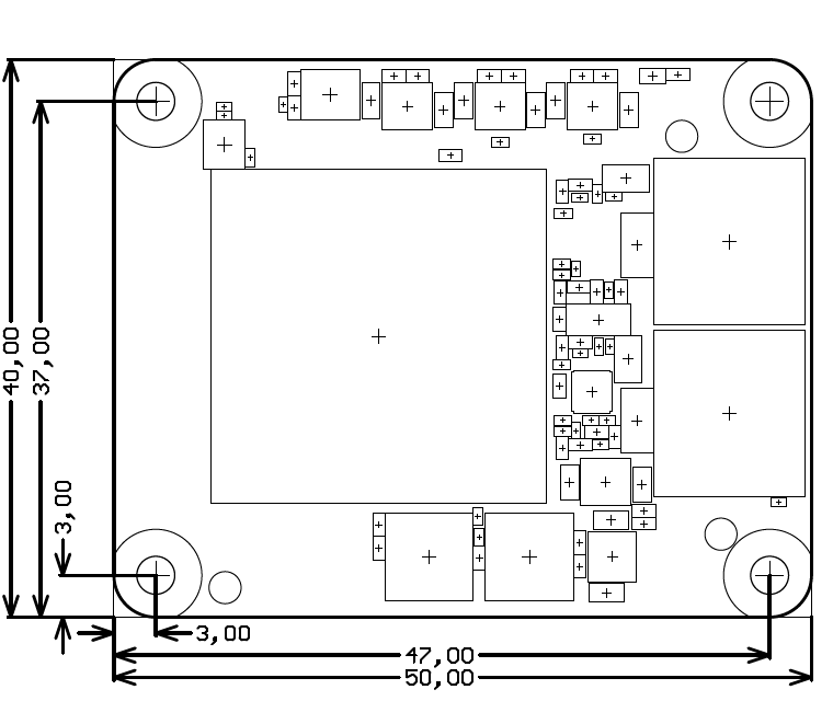
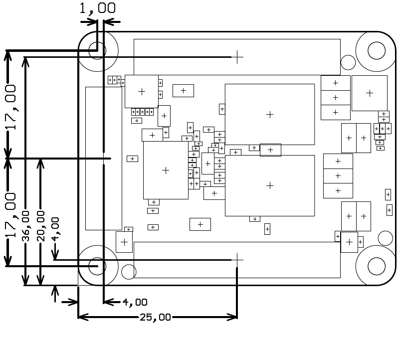
Physical Dimensions
Module size: 50 mm × 40 mm. Please download the assembly diagram for exact numbers.
Mating height with standard connectors: 8 mm.
PCB thickness: 1.6 mm.
Highest part on PCB: approximately 3 mm. Please download the step model for exact numbers.
All dimensions are given in millimeters.
Weight
47 g - Plain module.
9 g - Set of bolts and nuts.
Revision History
Hardware Revision History
| Date | Revision | Notes | PCN | Documentation Link |
|---|---|---|---|---|
| 2015-12-09 | 01 | First production revision | - | TE0841-01 |
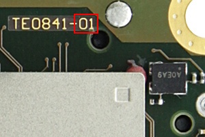
Hardware revision number is printed on the PCB board together with the module model number separated by the dash.
Document Change History
Date | Revision | Contributors | Description |
|---|---|---|---|
Jan Kumann | Initial document. |
Disclaimer
Data Privacy
Please also note our data protection declaration at https://www.trenz-electronic.de/en/Data-protection-Privacy
Document Warranty
The material contained in this document is provided “as is” and is subject to being changed at any time without notice. Trenz Electronic does not warrant the accuracy and completeness of the materials in this document. Further, to the maximum extent permitted by applicable law, Trenz Electronic disclaims all warranties, either express or implied, with regard to this document and any information contained herein, including but not limited to the implied warranties of merchantability, fitness for a particular purpose or non infringement of intellectual property. Trenz Electronic shall not be liable for errors or for incidental or consequential damages in connection with the furnishing, use, or performance of this document or of any information contained herein.
Limitation of Liability
In no event will Trenz Electronic, its suppliers, or other third parties mentioned in this document be liable for any damages whatsoever (including, without limitation, those resulting from lost profits, lost data or business interruption) arising out of the use, inability to use, or the results of use of this document, any documents linked to this document, or the materials or information contained at any or all such documents. If your use of the materials or information from this document results in the need for servicing, repair or correction of equipment or data, you assume all costs thereof.
Copyright Notice
No part of this manual may be reproduced in any form or by any means (including electronic storage and retrieval or translation into a foreign language) without prior agreement and written consent from Trenz Electronic.
Technology Licenses
The hardware / firmware / software described in this document are furnished under a license and may be used /modified / copied only in accordance with the terms of such license.
Environmental Protection
To confront directly with the responsibility toward the environment, the global community and eventually also oneself. Such a resolution should be integral part not only of everybody's life. Also enterprises shall be conscious of their social responsibility and contribute to the preservation of our common living space. That is why Trenz Electronic invests in the protection of our Environment.
REACH, RoHS and WEEE
REACH
Trenz Electronic is a manufacturer and a distributor of electronic products. It is therefore a so called downstream user in the sense of REACH. The products we supply to you are solely non-chemical products (goods). Moreover and under normal and reasonably foreseeable circumstances of application, the goods supplied to you shall not release any substance. For that, Trenz Electronic is obliged to neither register nor to provide safety data sheet. According to present knowledge and to best of our knowledge, no SVHC (Substances of Very High Concern) on the Candidate List are contained in our products. Furthermore, we will immediately and unsolicited inform our customers in compliance with REACH - Article 33 if any substance present in our goods (above a concentration of 0,1 % weight by weight) will be classified as SVHC by the European Chemicals Agency (ECHA).
RoHS
Trenz Electronic GmbH herewith declares that all its products are developed, manufactured and distributed RoHS compliant.
WEEE
Information for users within the European Union in accordance with Directive 2002/96/EC of the European Parliament and of the Council of 27 January 2003 on waste electrical and electronic equipment (WEEE).
Users of electrical and electronic equipment in private households are required not to dispose of waste electrical and electronic equipment as unsorted municipal waste and to collect such waste electrical and electronic equipment separately. By the 13 August 2005, Member States shall have ensured that systems are set up allowing final holders and distributors to return waste electrical and electronic equipment at least free of charge. Member States shall ensure the availability and accessibility of the necessary collection facilities. Separate collection is the precondition to ensure specific treatment and recycling of waste electrical and electronic equipment and is necessary to achieve the chosen level of protection of human health and the environment in the European Union. Consumers have to actively contribute to the success of such collection and the return of waste electrical and electronic equipment. Presence of hazardous substances in electrical and electronic equipment results in potential effects on the environment and human health. The symbol consisting of the crossed-out wheeled bin indicates separate collection for waste electrical and electronic equipment.
Trenz Electronic is registered under WEEE-Reg.-Nr. DE97922676.
Overview
Content Tools