Key Features
- Motor evaluation with an FPGA controller board, recommended with the Digilent Arty Z7 board
- Quick evaluation with reference motor board
- Power option up to 48V and 30A main supply current
Block Diagram
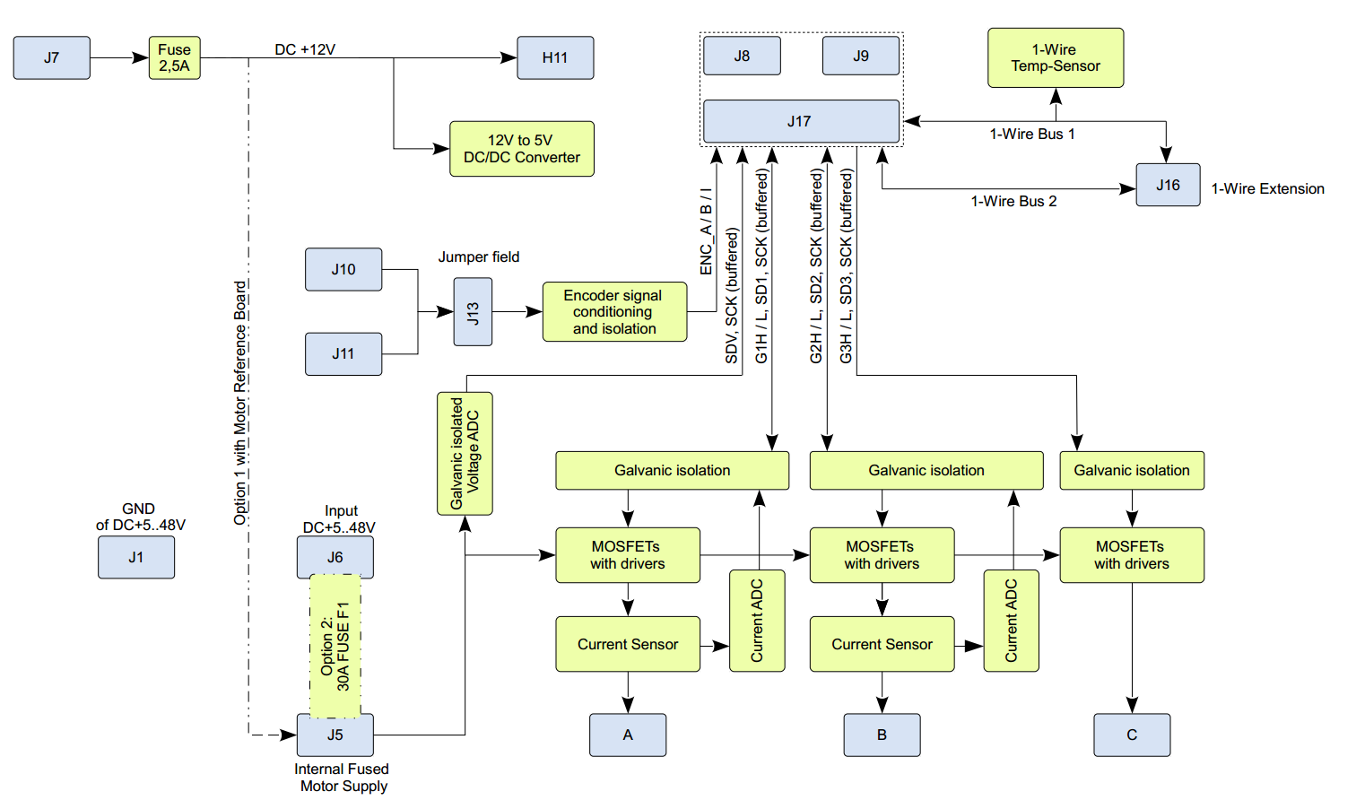
Main Components
- MOSFET drivers for 3-phase BLDC Motors
- Current measurement for 2-phases (3 phase measurement optional)
- Temperature sensor on board and 1-Wire bus external option
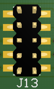
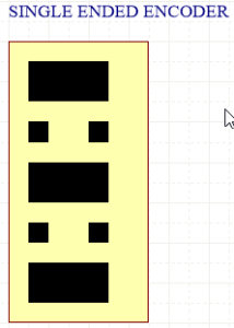
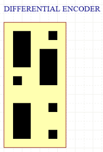
- Encoder input capable of receiving both single ended and differential signals
Scope of Delivery
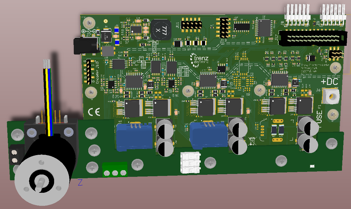
- The Eval Board comes with the already mounted and wired "Reference Motor Board"
- One "Arty Z7" Board: http://store.digilentinc.com/arty-z7-apsoc-zynq-7000-development-board-for-makers-and-hobbyists/usable with the reference FPGA IPs: TODO insert link
- Any DC +12V must be supplied to both boards supply connectors
(Two AC/DC Wall Mount Adapters are delivered as optional DC +12V power source) - One FUSE F1 30A for motor supply option 2
General Safety Instructions
- This product is only allowed to be used by an electrical specialist.
- This product is not allowed to be used unattended.
- There is a possible risk of burns due to hot surfaces while running the Board. This e.g. might be caused by an overcurrent at the motor outputs.
- All externally connected power sources must be SELV protected (Separated or safety extra-low voltage).
- For set up the wiring switch off or disconnect all external power supplies.
- During operations it is not allowed to change the wiring or mechanical setup.
- This product is only allowed to be used in a dry indoor environment.
- The product is only allowed to be used in horizontal position on a non-conducting and non-inflammable surface.
- The mechanical setup must ensure that the whole test setup can not be dropped to the floor or moved accidentally.
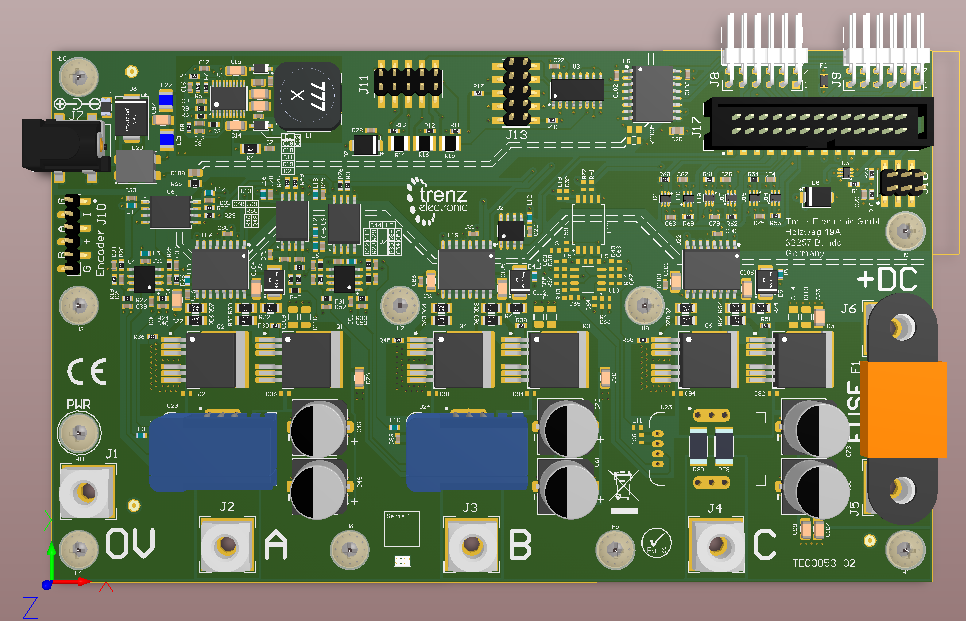
Signals, Interfaces and Pins
Control Board Connections
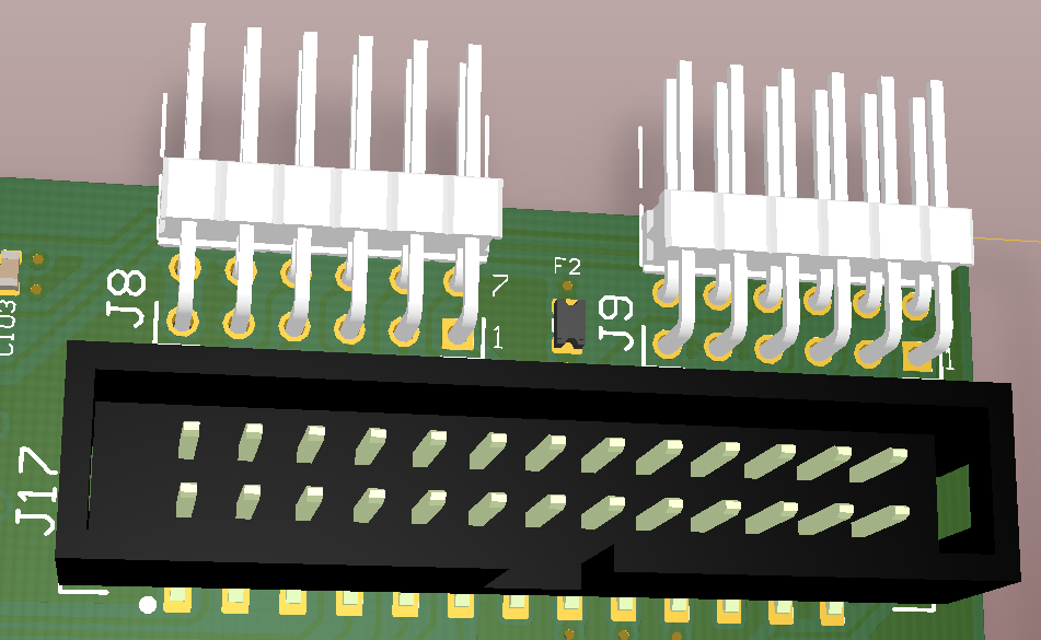
| Signal names | Connector J8 | Connector J9 | Connector J17 |
|---|---|---|---|
Digital Supply to EDPS | Pin 6, 12: +3.3V | Pin 6, 12: +3.3V Pin 5, 11: GND | Pin 5, 6, 21, 22: +3.3V Pin 1, 2, 25, 26: GND |
Motor Driver PWM Signals to EDPS High and Low Side control signals
| Pin 1: G1H - Ch.A HighSide | Pin 11: G1H - Ch.A HighSide | |
| ADC Clock Signal to EDPS | Pin 1: SCLK | Pin 23: SCLK | |
| Encoder Digital Signals from EDPS | Pin 8: ENC_A | Pin 20: ENC_A | |
| Motor Current ADC "raw" Signals from EDPS (usable with FPGA IP) | Pin 2: SDI1 - Current Ch.A | Pin 19: SDI1 - Current Ch.A | |
| Supply Voltage ADC "raw" Signal from EDPS (usable with FPGA IP) | Pin 7: SDIV - from DC_LINK | Pin 24: SDIV - from DC_LINK | |
| 1-Wire bus for temperature measurement | Pin 10: EXT1 - 1-Wire Bus 1 Pin 4: EXT2 - 1-Wire Bus 2 | Pin 4: EXT1 - 1-Wire Bus 1 | |
| Not connected pins | none | none | Pin 13, 14 |
Motor and Power Connections
There are two options available for the motor and power concept:
| Detail | Option 1: Reference Motor Board with DC +12V Supply | Option 2: Customer Motor at individual DC +5..48V | Comments |
|---|---|---|---|
| Motor Supply | From DC +12V Input J7 via Fuse F3 (TODO ... A) | From customer DC Supply to J6 via F1 on Eval Boad | |
| Motor Connection | Motor wires connected to cage clamps on Motor Reference Board J5 (A), J4 (B), J3 (C) | Motor wires connected to bolt screw terminals on Eval Board J2 (A), J3 (B), J4 (C) | |
| Encoder Connection | From encoder pins via ribbon cable to Eval Board J10, 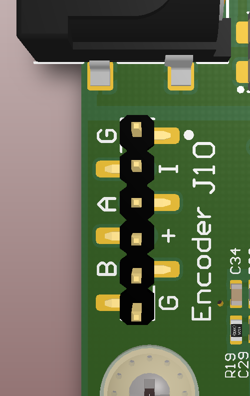 J11 single ended: | From motor to Eval Board J10 (only single ende signals) see left colomn, or to J11 (single OR differential signals): 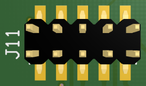 J11 single ended: J11 differential with 100R terminated: | Jumper Settings for encoder signals.
|
Internal
Temperature Sensor
Onboard is a Maxim 1-Wire Temperature sensor DS18S20Z+. This sensor is located in the middle of the PCB.
Addional 1-Wire temperature sensor(s) can be connected to the connector J16:
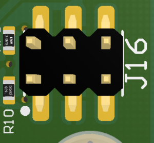
- Pin 1(DQ), 3 (GND),5 (+3.3V) at the same 1-wire bus as the onboard one
- Pin 2(DQ), 4 (GND),6 (+3.3V) at a separate 1-wire bus
Power and Power-On Sequence
Power Supply
DC 12V Supply Motor and Driver
The power source must be SELV (Separated or safety extra-low voltage) protected.
The motor drivers and the reference motor on the pre-mounted motor board TEC0060 are supplied by this voltage.
The internal +5V digital supply is generated from this +12V supply.
DC 5...48V Supply for Motor only
SAFETY INSTRUCTIONS:
Externally power supply for the motor must be SELV (Separated or safety extra-low voltage) protected.
This option is
- only allowed to be used for electrical specialist for the used electrical voltage and power conditions
- only allowed to be used under electrical laboratory conditions
- only allowed to be used in horizontal position on a non-conducting and non-inflammable surface
- only allowed to be used with a wiring, which fulfills the current rating for the maximum possible currents.
- only allowed to be used with a suitable current limiting circuit
- The maximum continuous current must not exceed 30A.
- The delivered fuse "Littelfuse Tpye 142.5631.5302" must be used as current limiter between connector J5 and J6.
- To limit the current for smaller motor loads an ADDITIONALLY appropriate current limiter can be used e.g. a current limited power source or a fuse integrated in the wiring.
- only allowed to be used with appropriate connectors at the M5 screw connectors, which means M5 cable lugs must be used and fastened according to technical standards.
- only allowed to be used, if the "Eval Boad high current signals" conducting up to 30A nominal, are covered by isolating, mechanically stable, non-inflammable (UL V-1 or better) material
The "Eval Boad high current signals" are the motor outputs A, B, C and Fuse F1 Connectors J5 an J6 and further internal connections shown white marked in the following picture:
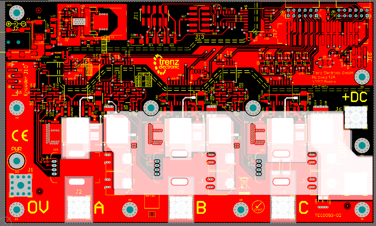
- As minimum protection it is mandatory to use the delivered "Isolating cover PCB" (marked in green), which must be mounted to the mounting holes H1, H9, H3, H4 with the delivered 10mm isolating spacers:
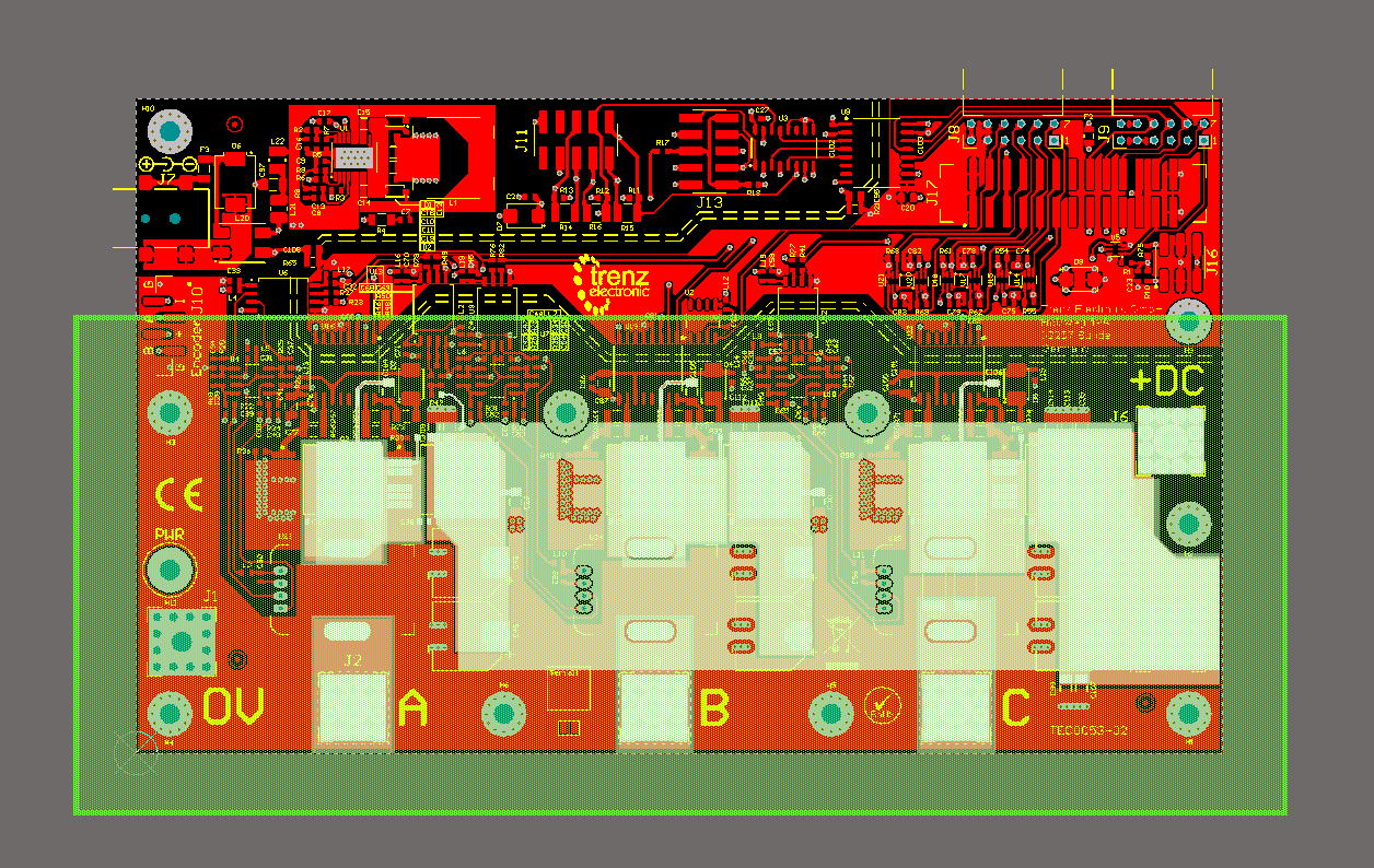
- The used cable lugs need to be isolated in the area outstanding the outer border of the Eval Board.
Make sure that the "Isolating Cover PCB" is overlapping the conducting material by a minimum of 20 mm.
Initial operation
To use a separate power supply for the motor supply perform the following steps:
- Disconnect the reference motor board TEC0060 by unmounting its screws and the encoder cable from J10
- Mount the delivered 30A fuse to the connectors J5 and J6 with the delivered M5 screws
- For lower supply current requirements, caused by the power rating of the used motor, a fuse with a lower and suitable current rating integrated in the supply wiring is recommended.
- Connect with cable lugs the +DC 5..48V to J6 and the corresponding GND to J1.
- The cable length is limited to 3m.
- Connect the three motor phases to J2 (A), J3 (B) and J4 (C).
- The cable length is limited to 3m.
- Optional: connect the encoder to J10 or J11 and set jumper field according to signal specification: differential or single ended. See section TODO for details.
Power Consumption
Test Condition:
| VIN Current mA | Notes |
|---|---|---|
| TEC0053-03 +3V3 | TODO mA | |
| TEC0053-03 +12V | TODO mA |
Power-On Sequence
Any power sequence of the three supply sources is allowed:
- +3V3 Supply from the FPGA Board, generated by FPGA Board supply
- +12V and
- optional +5..48V Motor Supply
Reference Motor Board TEC0060
For easy connection of the reference Motor and Encoder to the Driver board a special Motor Adapter Board TEC0060 is included in the EDDP Kit.
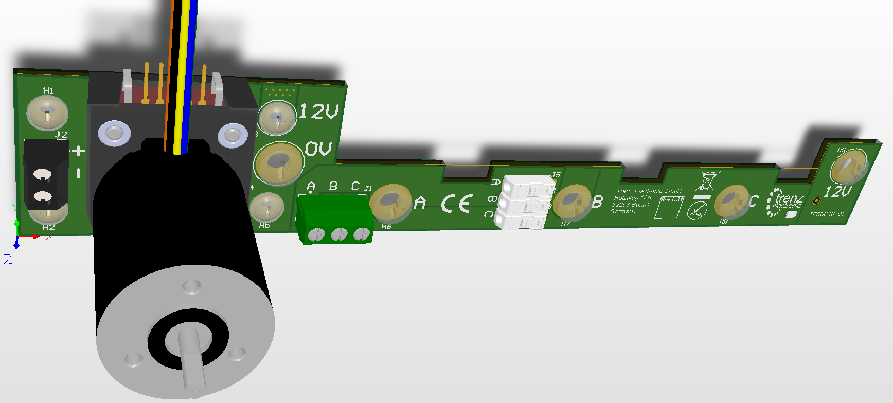
Reference Motor
The reference motor is manufactured by Anaheim Automation. The order code for the motor with the encoder already mounted is BLWR111D-24V-10000-1000SI. Please note that the encoder is not available separately. The nominal motor voltage is DC 24V, however, only 12V is supplied by the Reference Motor Board, which results in reduced performance.
The datasheet for the motor can be found at
http://www.anaheimautomation.com/manuals/brushless/L010234%20-%20BLWR11%20Series%20Product%20Sheet.pdf
The datasheet for the encoder can be found at
http://www.anaheimautomation.com/manuals/accessories/L010390%20-%20Single%20Ended%20Encoder%20with%20Index%20Channel.pdf
WIP section
Technical Specifications
Absolute Maximum Ratings
| Parameter | Min | Max | Units | Notes | Reference document |
|---|---|---|---|---|---|
DC +12V supply | 0 | 38 | V | LM20242 datasheet | |
| DC +5..48V supply | 0 | 80V | V | IPB015N08N5 datasheet | |
| DC +3V3 supply | -0.5 | 6 | V | DS18S20Z datasheet | |
| PWM Input | -0.5 | 6.5 | V | SN74LVC1G97 datasheet | |
| ADC Digital Input | -0.5 | 3.8 | V | DC +3V3 = 3.3V | AD7403 datasheet |
| Encoder Input | -7 | 12 | V | SN65LBC173AD datasheet |
Recommended Operating Conditions
| Parameter | Min | Max | Units | Notes | Reference document |
|---|---|---|---|---|---|
DC +12V supply | 11.5 | 12.5 | V | ||
| DC +5..48V supply | 5 | 48 | V | ||
| DC +3V3 supply | 3.0 | 3.6 | V | DS18S20Z datasheet | |
| PWM Input | 0 | DC +3V3 supply | V | ||
| ADC Digital Input | 0 | DC +3V3 supply | V | ||
| Encoder Input | -7 | 12 | V | SN65LBC173AD datasheet |
Electrical characteristics
DC +3V3 supply = 3.3V
| Parameter | Min | Max | Units | Notes | Reference document |
|---|---|---|---|---|---|
| PWM Input Logic High Level | 2.2 | V | SN74LVC1G97 datasheet | ||
| PWM Input Logic Low Level | 0.8 | V | SN74LVC1G97 datasheet | ||
| ADC Digital Input Logic High Level | 2.7 | V | AD7403 datasheet | ||
| ADC Digital Input Logic Low Level | 0.6 | V | AD7403 datasheet | ||
| ADC Digital Output Logic High Level | 3.2 | 3.3 | V | Io=-200μA | AD7403 datasheet |
| ADC Digital Output Logic Low Level | 0 | 0.4 | V | Io=+200μA | AD7403 datasheet |
| Encoder Input Logic High Level (Differential) | -0.2 | V | SN65LBC173AD datasheet | ||
| Encoder Input Logic Low Level (Differential) | -0.01 | V | SN65LBC173AD datasheet | ||
| Encoder Input Logic High Level (Single Ended) | 2 | V | SN65LBC173AD datasheet | ||
| Encoder Input Logic Low Level (Single Ended) | 0.6 | V | SN65LBC173AD datasheet |
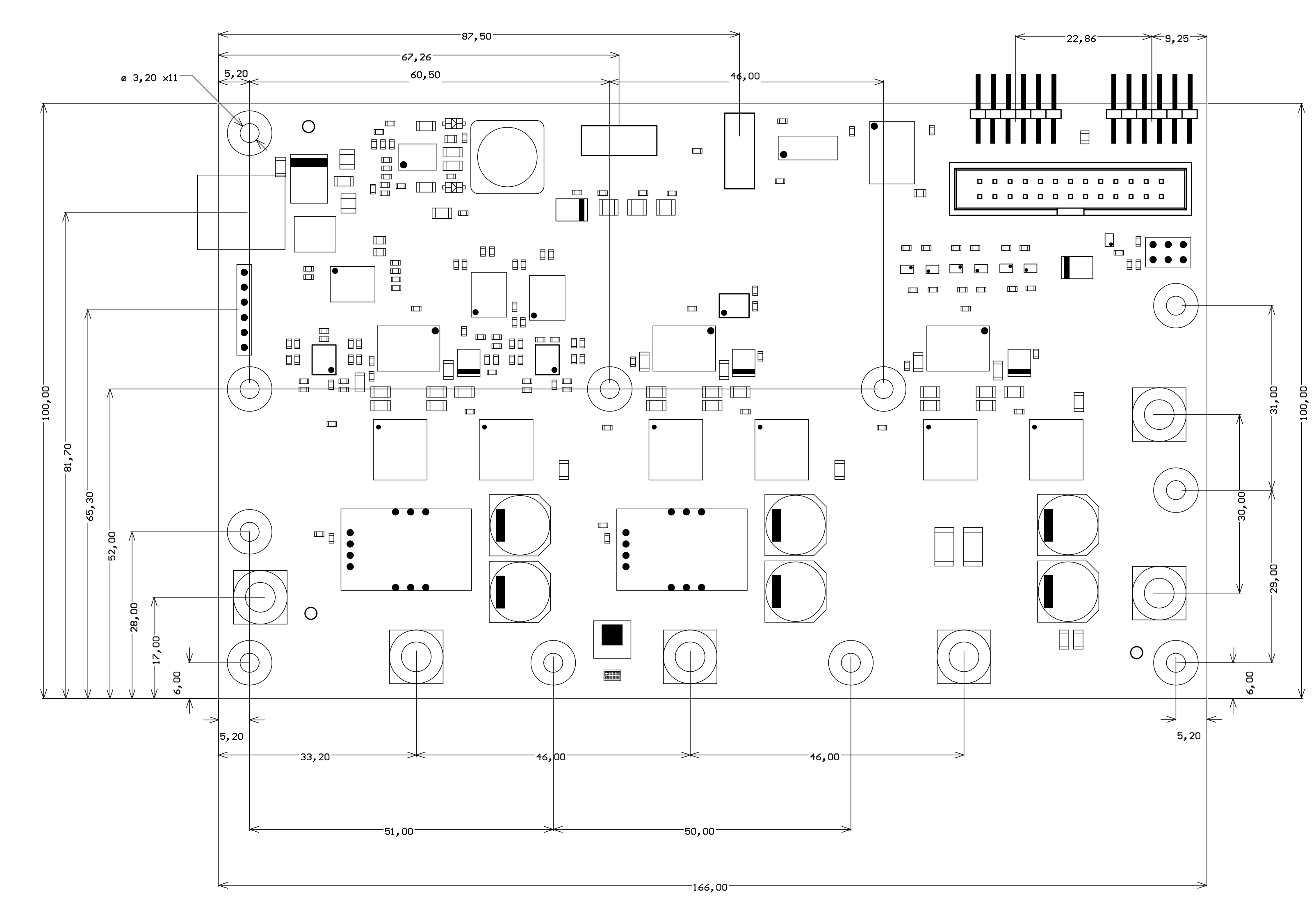
Physical Dimensions
Board size: 100 mm × 166 mm. Please download the assembly diagram for exact numbers.
PCB thickness: 1.75 mm +/-10%
Highest part on PCB: approximately 17 mm. Please download the step model for exact numbers.
All dimensions are shown in mm. Additional sketches, drawings and schematics can be found TODO: here.
Operating Temperature Ranges - TODO
Weight - TODO
| Variant | Weight in g | Note |
|---|---|---|
| - | TODO |
|
Revision History
Hardware Revision History - TODO
| Date | Revision | Notes | PCN Link | Documentation Link |
|---|---|---|---|---|
| 2016-03-27 | 02 | TEC0053-02 | ||
| 2017-08-14 | 04 |
Hardware revision number is printed on the PCB board in the down right corner.
Document Change History - TODO
Date | Revision | Authors | Description |
|---|---|---|---|
| 2017-03-30 |
| Andreas Heidemann | Initial Version |
Overview
Content Tools