Table of Contents
<!-- Template Revision 1.63 (HTML comment will not display, it's not needed to remove them. For Template/Skeleton changes, increase Template Revision number. So we can check faster, if the TRM style is up to date) --> |
Download PDF version of this document. |
Table of Contents |
Refer to https://wiki.trenz-electronic.de/display/DRAFT/TE0722+TRM for downloadable version of this manual and additional technical documentation of the product. |
The Trenz Electronic TE0722-02 is a DIPFORTy1 "Soft Propeller" based on the Xilinx Zynq-7000 SoC.
Additional assembly options are available for cost or performance optimization upon request.
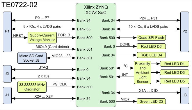
Figure 1: TE022-02 block diagram.
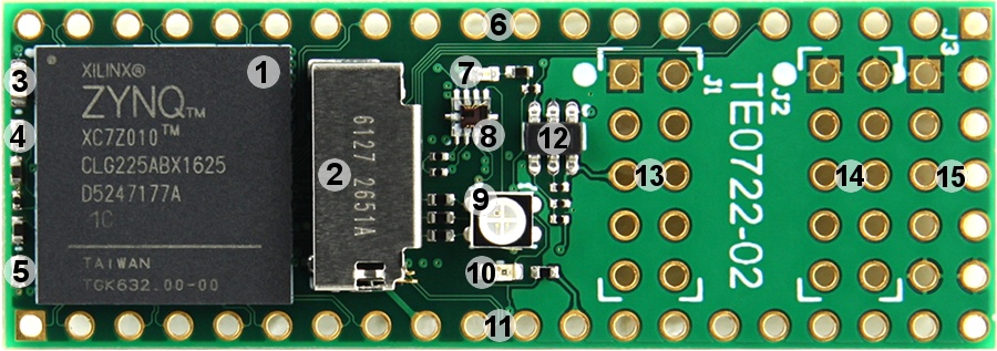
Figure 2: TE0722-02 PCB top side.
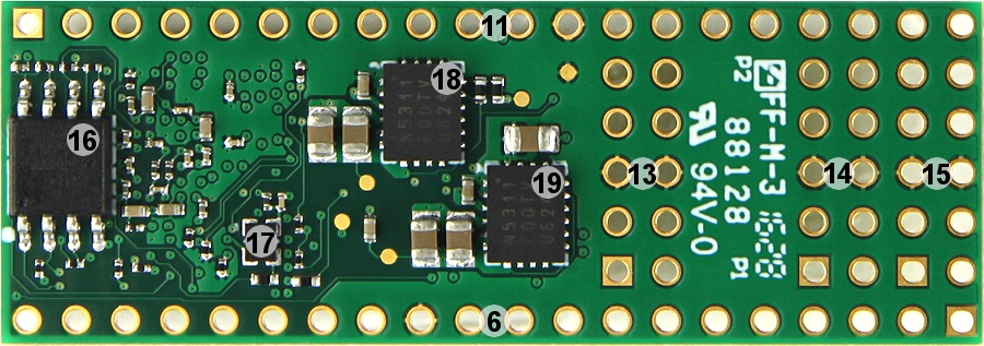
Figure 3: TE0722-02 PCB bottom side.
Storage device name | Content | Notes |
|---|---|---|
Quad SPI Flash | Empty |
Table 1: .
By default the ... supports QSPI and SD Card boot modes which is controlled by the MODE input signal from the B2B connector JM..
High or open | SD Card |
Low or ground | QSPI Interface |
Table 2: Selecting power-on boot device.
Overview of the PL I/O banks signals routed to the external connectors:
| Bank | Type | Connector | I/O Signal Count | Voltage | Notes |
|---|---|---|---|---|---|
| 34 | HR | P1 | 8 | 3.3 | P0 - P7 |
| 34 | HR | P2 | 8 | 3.3 | P24 - P31 |
| 34 | HR | P2 | 10, 5 LVDS pairs | 3.3 | |
| 34 | HR | J1 | 6 | 3.3 | X2A - X2F |
| 34 | HR | J2 | 2 | 3.3 | |
| 34 | HR | J3 | 4 | 3.3 | X1A - X1D |
| 35 | HR | P1 | 8, 4 LVDS pairs | 3.3 |
Table 3: PL I/O signals overview.
JTAG access to the Xilinx ZYNQ XC7Z010 SoC is provided through J2 connector.
JTAG Signal | J2 Connector Pin |
|---|---|
| TCK | 4 |
| TDI | 9 |
| TDO | 10 |
| TMS | 8 |
Table 4: JTAG interface signals.
Quad SPI Flash (U5) is connected to the Zynq PS QSPI0 interface via PS MIO bank 500, pins MIO1 ... MIO6.
| Zynq SoC's MIO | Signal Name | U5 Pin |
|---|---|---|
| 1 | SPI0_CS | 1 |
| 2 | SPI0_DQ0/MIO2 | 5 |
| 3 | SPI0_DQ1/MIO3 | 2 |
| 4 | SPI0_DQ2/MIO4 | 3 |
| 5 | SPI0_DQ3/MIO5 | 7 |
| 6 | SPI0_SCK | 6 |
Table 3: Quad SPI interface signals and connections.
TE0723 module has on-board 3.3V SD Card socket (J10) with card detect switch wired to the SoC PS MIO bank 500.
| Zynq SoC's Pin | Connected To | Signal Name |
|---|---|---|
| MIO0 | J10-9 | Card detect switch |
| MIO10 | J10-7 | DAT0 |
| MIO11 | J10-3 | CMD |
| MIO12 | J10-5 | CLK |
| MIO13 | J10-8 | DAT1 |
| MIO14 | J10-1 | DAT3 |
| MIO15 | J10-2 | CD/DAT3 |
Table 4: SD card socket signals.
I2C interface pins SCL and SDA from the Zynq SoC PL bank 34 are connected to the connector J1. There are no on-board I2C slave devices.
| Zynq SoC's Pin | Connected To | Signal Name |
|---|---|---|
| R13 | J1-9 | SDA |
| P13 | J1-10 | SCL |
Table 7: Zynq SoC I2C interface.
I2C interface pins SCL and SDA from the Zynq SoC PL bank 34 are connected to the connector J1. There are no on-board I2C slave devices.
| Zynq SoC's Pin | Connected To | Signal Name |
|---|---|---|
| R13 | J1-9 | SDA |
| P13 | J1-10 | SCL |
Table 7: Zynq SoC I2C interface.
| MIO | Function | Connector Pin | Notes |
|---|---|---|---|
| 0 | - | - | - |
| 1 | QSPI | - | SPI Flash-CS |
| 2 | QSPI | - | SPI Flash-DQ0 |
| 3 | QSPI | - | SPI Flash-DQ1 |
| 4 | QSPI | - | SPI Flash-DQ2 |
| 5 | QSPI | - | SPI Flash-DQ3 |
| 6 | QSPI | - | SPI Flash-SCK |
| 7 | GPIO | - | Green LED D2 |
| 8 | - | - | - |
| 9 | - | - | - |
| 28 | SD CARD | J8-5 | CLK |
| 29 | SD CARD | J8-3 | CMD |
| 30 | SD CARD | J8-7 | DAT0 |
| 31 | SD CARD | J8-8 | DAT1 |
| 32 | SD CARD | J8-1 | DAT2 |
| 33 | SD CARD | J8-2 | CD/DAT3 |
| 36 | I2C | - | SCL |
| 37 | I2C | - | SDA |
| 39 | GPIO | - | Si1143 INT pin |
| 49 | SD CARD | J8-G4 | Card detect switch |
Table 5: .
| LED | Color | Connected To | Description and Notes |
|---|---|---|---|
| D1 | Red | LED2, U4 | |
| D2 | Green | MIO7, U1 | User controlled, default OFF (when PS7 has not been booted). |
| D3 | Red | LED1, U4 | |
| D4 | RGB | RGB_R, U1 RGB_G, U1 RGB_B, U1 | |
| D5 | Red | LED3, U4 | |
D6 | Green | DONE, U1 | Reflects inverted DONE signal. ON when FPGA is not configured, OFF as soon as PL configuration is finished. |
Table 6: .
The maximum power consumption of the module mainly depends on the design running on the Zynq SoC's FPGA.
Xilinx provide a power estimator excel sheets to calculate power consumption. It is also possible to evaluate the power consumption of the developed design with Vivado. See also Trenz Electronic Wiki FAQ.
| Power Input | Typical Current |
|---|---|
| 3.3V | TBD* |
Table 7: Typical power consumption.
* TBD - To Be Determined.
Power supply with minimum current capability of 1A for system startup is recommended.
... diagram will be here soon ...
| Module Variant | Xilinx Zynq SoC | ARM Cores | PL Cells | LUTs | Flip-Flops | Block RAM | DSP Slices | Operating Temperature | Temperature Range |
|---|---|---|---|---|---|---|---|---|---|
| TE0722-02I | XC7Z010-1CLG225I | Dual-core | 28K | 17,6K | 35,2K | 2.1 MBytes | 80 | –40°C to +85°C | Industrial |
| TE0722-02 | XC7Z010-1CLG225C | Dual-core | 28K | 17,6K | 35,2K | 2.1 MBytes | 80 | 0°C to +70°C | Commercial |
| TE0722-02-07S-1C | XC7Z007S-1CLG225C | Single-core | 23K | 14,4K | 28,8K | 1.8 MBytes | 66 | 0°C to +70°C | Commercial |
Table 8: Module variants.
Parameter | Min | Max | Units | Reference Document |
|---|---|---|---|---|
VIN supply voltage | -0.5 | 3.6 | V | Xilinx datasheet DS187, "Zynq-7000 All Programmable SoC: DC and AC Switching Characteristics". |
Storage temperature | -40 | +85 | °C | Silicon Labs Si1141/42/43 datasheet. |
Table 9: Module absolute maximum ratings.
| Parameter | Min | Max | Units | Reference Document |
|---|---|---|---|---|
| Supply voltage | 1.14 | 3.465 | V | Xilinx datasheet DS187, "Zynq-7000 All Programmable SoC: DC and AC Switching Characteristics". |
Table 10: Module recommended operating conditions.
| Assembly variants for higher storage temperature range are available on request. |
Module size: 18 mm × 51 mm. Please download the assembly diagram for exact numbers.
PCB thickness: 1.6 mm.
Highest part on PCB approx. 4 mm. Please download the step model for exact numbers.
All dimensions are given in millimeters.
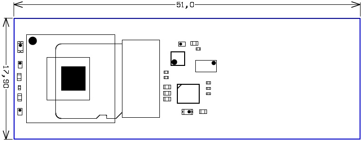
Figure 4: TE0722-02 physical dimensions.
Commercial grade: 0°C to +70°C.
Industrial grade: -40°C to +85°C.
Operating temperature range depends also on customer design and cooling solution. Please contact us for options.
| Date | Revision | Notes | PCN | Documentation Link |
|---|---|---|---|---|
| 2015-10-23 | 02 | TE0722-02 | ||
01 |
|
Table 11: TE0722 module hardware revision history.
Hardware revision number is printed on the PCB board together with the module model number separated by the dash.
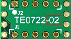
Figure 5: TE0722 module hardware revision number.
Date | Revision | Contributors | Description |
|---|---|---|---|
Jan Kumann | Initial document. |
Table 12: Document change history.