some sources available on public doc TEBT0808 TRM

Template Revision 2.5

  • Module: TRM Name always "TE Series Name" +TRM
    Example: "TE0728 TRM"
  • Carrier: TRM Name usually "TEB Series Name" +TRM
    Example: "TEB0728 TRM"


<!-- tables have all same width (web max 1200px and pdf full page(640px), flexible width or fix width on menu for single column can be used as before) -->
<style>
.wrapped{
  width: 100% !important;
  max-width: 1200px !important;
 }
</style>


Important General Note:

  • If some section is configurable and depends on Firmware, please refer to the addition page (for example CPLD). If not available, add note, that this part is configurable
  • Designate all graphics and pictures with a number and a description, Use "Scroll Title" macro

    • Use "Scroll Title" macro for pictures and table labels. Figure number must be set manually at the moment (automatically enumeration is planned by scrollPDF)
      • Figure template:


        Create DrawIO object here: Attention if you copy from other page, objects are only linked.


        image link to the generate DrawIO PNG file of this page. This is a workaround until scroll pdf export bug is fixed


      • Table template:

        • Layout macro can be use for landscape of large tables

      • ExampleComment
        12


    • The anchors of the Scroll Title should be named consistant across TRMs. A incomplete list of examples is given below

      • <type>_<main section>_<name>

        • type: Figure, Table
        • main section:
          • "OV" for Overview
          • "SIP" for Signal Interfaces and Pins,
          • "OBP" for On board Peripherals,
          • "PWR" for Power and Power-On Sequence,
          • "B2B" for Board to Board Connector,
          • "TS" for Technical Specification
          • "VCP" for Variants Currently in Production
          •  "RH" for Revision History
        • name: custom, some fix names, see below
      • Fix names:
        • "Figure_OV_BD" for Block Diagram

        • "Figure_OV_MC" for Main Components

        • "Table_OV_IDS" for Initial Delivery State

        • "Table_PWR_PC" for Power Consumption

        • "Figure_PWR_PD" for Power Distribution
        • "Figure_PWR_PS" for Power Sequence
        • "Figure_PWR_PM" for Power Monitoring
        • "Table_PWR_PR" for Power Rails
        • "Table_PWR_BV" for Bank Voltages
        • "Table_TS_AMR" for Absolute_Maximum_Ratings

        • "Table_TS_ROC" for Recommended_Operating_Conditions

        • "Figure_TS_PD" for Physical_Dimensions
        • "Table_VCP_SO" for TE_Shop_Overview
        • "Table_RH_HRH" for Hardware_Revision_History

        • "Figure_RH_HRN" for Hardware_Revision_Number
        • "Table_RH_DCH" for Document_Change_History
    • Use Anchor in the document: add link macro and add "#<anchorname>
    • Refer to Anchror from external : <page url>#<pagename without space characters>-<anchorname>


-----------------------------------------------------------------------


Note for Download Link of the Scroll ignore macro:


Download PDF version of this document.


Table of Contents

Overview

The Trenz Electronic TEBT0808-01 is a testboard for module TE0808 (REV 02 and 03) as well as for TE0803 (REV 01).

Refer to http://trenz.org/tebt0808-info for the current online version of this manual and other available documentation.

Notes :

Key Features

Note:
Use 'Key Features' description in shoping page, for example: https://shop.trenz-electronic.de/de/TE0728-04-1Q-SoC-Micromodul-mit-Xilinx-Automotive-Zynq-7020-512-MByte-DDR3L-6-x-6-cm

Supported Bootmodes are SPI and JTAG.

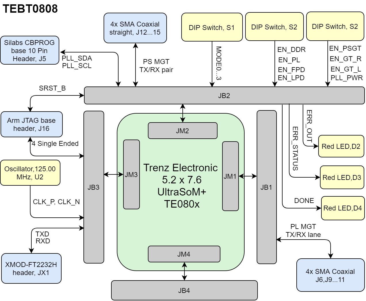
Block Diagram

add drawIO object here.

For more information regarding how to draw a diagram, Please refer to "Diagram Drawing Guidline" .


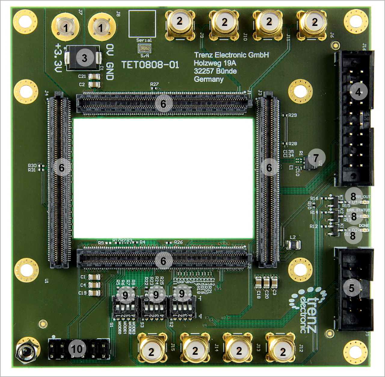
Main Components

Notes :

  • Picture of the PCB (top and bottom side) with labels of important components
  • Add List below


For more information regarding how to add board photoes, Please refer to "Diagram Drawing Guidline" .


  1. Uninsulated 2 mm rigid socket. J8-J7
  2. SMA Coaxial straight. J6- J9...15
  3. Surface Mount Schottky Barrier Rectifier. D1
  4. Box Headers, Straight/Angled J5-J16
  5. Board to Board Connector. J1...4
  6. Clock Oscillator, U2
  7. On-Board LED, D2...4
  8. DIP-Switch, S1...3
  9. XMOD JTAG Base, 

Initial Delivery State

Notes :

Only components like EEPROM, QSPI flash and DDR3 can be initialized by default at manufacture.

If there is no components which might have initial data ( possible on carrier) you must keep the table empty


Storage device name

Content

Notes


Configuration Signals

  • Overview of Boot Mode, Reset, Enables.

Boot mode can be set by DIP-Switch S1.

M3M2M1M0Bootmode HexBootmodeNotes
ONONONON0x0PS Main JTAG (TE0790 USB JTAG)Needed for SPI Flash Programming
ONONOFFON0x2SPI Flash (dual parallel, 4bit x 2, 32bit Addressing)Default


Signal

B2BNote

PLL_RST

J2-89
SRST_BJ2-96connected to PJTAG0_SRST - J16


Signals, Interfaces and Pins

Notes :

  • For carrier or stand-alone boards use subsection for every connector type (add designator on description, not on the subsection title), for example:
    • SD
    • USB
    • ETH
    • FMC
    • ...
  • For modules which needs carrier use only classes and refer to B2B connector if more than one is used, for example
    • JTAG
    • UART
    • I2C
    • MGT
    • ...

Board to Board (B2B) I/Os

FPGA bank number and number of I/O signals connected to the B2B connector:

B2B ConnectorInterfacesNumber of I/ONotes
J1

User I/O

22 singel ended, 11 Differential

8 singel ended, 4 Differential

8 singel ended, 4 Differential

8 singel ended, 4 Differential

3 singel ended

Connected to Bank 66

Connected to Bank 228

Connected to Bank 229

Connected to Bank 230

VCCO_66, PL_1V8

J2

Ethernet PHY

32 singel ended, 16 Differential

4 singel ended, 16 Differential

Connected to Bank 505

Connected to Bank 128

Control Signals15 single endedPLL_SEL0, PLL_SEL1, PLL_RST, EN_GTR, EN_PL, PLL_LOLN, EN_PSGT, ERR_STATUS, ERR_OUT,SRST_B, INIT_B, PROG_B, EN_FPD , EN_LPD , DONE
Power Control Signal10 single endedEN_PLL_PWR, PLL_FINC ,PG_PLL_1V8, LP_GOOD, PG_DDR, PG_PL, PG_FPD, PG_PSGT, PG_GT_R, PG_GT_L
JTAG Interface7 single endedTCK, TDI, TMS, TDO, MR, Rxd, Txd
WANNE22 single endedPLL_SCL, PLL_SDA
Clock

6 singel ended, 3 Differential

CLK0, CLK7, CLK8

J3


User I/O

12 singel ended, 6 Differential

12 singel ended, 6 Differential

Connected to Bank 48

Connected to Bank 47

Clock6 singel ended, 3 DifferentialCLK228, CLK229, CLK230
PJTAG Interface7 single endedPJTAG0_TCK, PJTAG0_TDI, PJTAG0_TMS, PJTAG0_TDO,
MIO27 single endedMIO19..76
UART2 single endedTXD, RXD
Power pins4 single endedPS_1V8, SI_PLL_1V8, VCCO_48, VCCO_47
J4User I/O

48 singel ended, 62 Differential

4 single ended

Connected to Bank 64

Connected to Bank 64

Power pins4 single endedVCCO_64, VCCO65


JTAG Interface

JTAG access to the TExxxx SoM through B2B connector JMX.

JTAG Signal

B2B Connector

TMSJ2-126
TDIJ2-122
TDOJ2-124
TCK

J2-120

MRJ2-83
RXDJ3-141
TXDJ3-139


On-board Peripherals

Notes :

  • add subsection for every component which is important for design, for example:
    • Two 100 Mbit Ethernet Transciever PHY
    • USB PHY
    • Programmable Clock Generator
    • Oscillators
    • eMMCs
    • RTC
    • FTDI
    • ...
    • DIP-Switches
    • Buttons
    • LEDs


Notes :

In the on-board peripheral table "chip/Interface" must be linked to the corresponding chapter or subsection


Chip/InterfaceDesignatorNotes


DIP Switch

There are thre DIP Switches, S1, S2, S3.

The Boot Mode can be set through DIP Switch S1, refer to Boot Mode table.

Signals

B2B

S1 switchNotes
MODE0J2-109S1A
MODE1J2-107S1B
MODE2J2-105S1C
MODE3J2-103S1D


SignalsB2BS2 switchNotes
EN_PSGTJ2-84S2A
EN_GT_RJ2-95S2B
EN_GT_LJ2-97S2C
EN_PLL_PWRJ2-77S2Dconnected to PG_PL


SignalsB2BS3 switchNotes
EN_DDRJ2-112S3A
EN_LPDJ2-108S3B
EN_PLJ2-101S3C
EN_FPDJ2-102S3D


LEDs

DesignatorColorConnected toActive LevelNote
D2RedDONELow
D3RedERR_STATUSLow
D4RedERR_OUTLow


Ethernet

BankSignal NameETH1ETH2Signal Description


CAN Transceiver

BankSchematicU?? PinNotes

D-Tx
Driver Input

R-Rx
Reciever Output


Clock Sources

DesignatorDescriptionFrequencyNote
U2MEMS Oscillator125.00 MHz


Power and Power-On Sequence

In 'Power and Power-on Sequence' section there are three important digrams which must be drawn:

  • Power on-sequence
  • Power distribution
  • Voltage monitoring circuit


For more information regarding how to draw diagram, Please refer to "Diagram Drawing Guidline" .


Power Supply

Power supply with minimum current capability of xx A for system startup is recommended.

Power Consumption

Power Input PinTypical Current
VINTBD*


* TBD - To Be Determined

Power Distribution Dependencies


Create DrawIO object here: Attention if you copy from other page, objects are only linked.


image link to the generate DrawIO PNG file of this page. This is a workaround until scroll pdf export bug is fixed


Power-On Sequence


Create DrawIO object here: Attention if you copy from other page, objects are only linked.


image link to the generate DrawIO PNG file of this page. This is a workaround until scroll pdf export bug is fixed


Voltage Monitor Circuit


Create DrawIO object here: Attention if you copy from other page, objects are only linked.


image link to the generate DrawIO PNG file of this page. This is a workaround until scroll pdf export bug is fixed


Power Rails


Power Rail Name

B2B Connector

JM1 Pin

B2B Connector

JM2 Pin

B2B Connector

JM3 Pin

DirectionNotes


Bank Voltages

Bank          

Schematic Name

Voltage

Notes


Board to Board Connectors

  • This section is optional and only for modules.
  • use "include page" macro and link to the general B2B connector page of the module series,

    For example: 6 x 6 SoM LSHM B2B Connectors

? x ? modules use two or three Samtec Micro Tiger Eye Connector on the bottom side.

Technical Specifications

Absolute Maximum Ratings

SymbolsDescriptionMinMaxUnit


V


V


V


V


V


V


V


V


Recommended Operating Conditions

Operating temperature range depends also on customer design and cooling solution. Please contact us for options.

ParameterMinMaxUnitsReference Document


VSee ???? datasheets.


VSee Xilinx ???? datasheet.


VSee Xilinx ???? datasheet.


VSee Xilinx ???? datasheet.


VSee Xilinx ???? datasheet.


VSee Xilinx ???? datasheet.


VSee Xilinx ???? datasheet.


°CSee Xilinx ???? datasheet.


°CSee Xilinx ???? datasheet.


Physical Dimensions

PCB thickness: ?? mm.

In 'Physical Dimension' section, top and button view of moduloe must be insterted, information regarding physical dimention can be obtained through webpage for product in Shop.Trenz, (Download> Documents> Assembly part)for every SoM.

For Example: for Module TE0728, Physical Dimension information can be captured by snipping tools from the link below:

https://www.trenz-electronic.de/fileadmin/docs/Trenz_Electronic/Modules_and_Module_Carriers/5.2x7.6/TE0745/REV02/Documents/AD-TE0745-02-30-1I.PDF

For more information regarding how to draw diagram, Please refer to "Diagram Drawing Guidline" .


Create DrawIO object here: Attention if you copy from other page, objects are only linked.


image link to the generate DrawIO PNG file of this page. This is a workaround until scroll pdf export bug is fixed


Currently Offered Variants 

Set correct link to the shop page overview table of the product on English and German.

Example for TE0728:

ENG Page: https://shop.trenz-electronic.de/en/Products/Trenz-Electronic/TE07XX-Zynq-SoC/TE0728-Zynq-SoC/

DEU Page: https://shop.trenz-electronic.de/de/Produkte/Trenz-Electronic/TE07XX-Zynq-SoC/TE0728-Zynq-SoC/

if not available, set.


Trenz shop TE0728 overview page
English pageGerman page


Revision History

Hardware Revision History

DateRevisionNotePCN
-

-


Document Change History

  • Note this list must be only updated, if the document is online on public doc!
  • It's semi automatically, so do following
    • Add new row below first

    • Copy "Page Information Macro(date)" Macro-Preview, Metadata Version number, Author Name and description to the empty row. Important Revision number must be the same as the Wiki document revision number Update Metadata = "Page Information Macro (current-version)" Preview+1 and add Author and change description. --> this point is will be deleted on newer pdf export template

    • Metadata is only used of compatibility of older exports


DateRevisionContributorDescription


  • change list

--

all

  • --


Disclaimer