Overview
The Trenz Electronic TE0710 is an industrial-grade FPGA module integrating a Xilinx Artix-7 T FPGA, dual 100 MBit Ethernet transceivers, 512 MByte DDR3 SDRAM with 8-bit width, 32 megabyte Flash memory for configuration and operation and powerful switch-mode power supplies for all on-board voltages. A large number of configurable I/Os is provided via rugged high-speed stacking strips. All modules in 4 x 5 cm form factor are mechanically compatible.
All this on a tiny footprint, smaller than a credit card, at the most competitive price.
Key Features
Industrial-grade Xilinx Artix-7 (15T to 100T) SoM (System on Module), supported by the free Xilinx Vivado WebPACK tool
Rugged for shock and high vibration
512 MByte DDR3 SDRAM
Dual 100 MBit Ethernet PHY
MAC Address EEPROM
32 MByte QSPI Flash memory (with XiP support)
100 MHz programmable MEMS oscillator
Plug-on module with 2 × 100-pin high-speed hermaphroditic strips
112 FPGA I/Os (51 differential pairs) and available on board-to-board connectors
On-board high-efficiency DC-DC converters
4.0 A x 1.0 V power rail
1.0 A x 1.8 V power rail
1.0 A x 1.5 V power rail
System management and power sequencing
eFUSE bit-stream encryption
AES bit-stream encryption
User LED
Evenly-spread supply pins for good signal integrity
Assembly options for cost or performance optimization available upon request.
Board Components
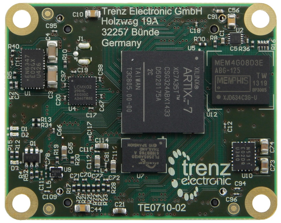
| 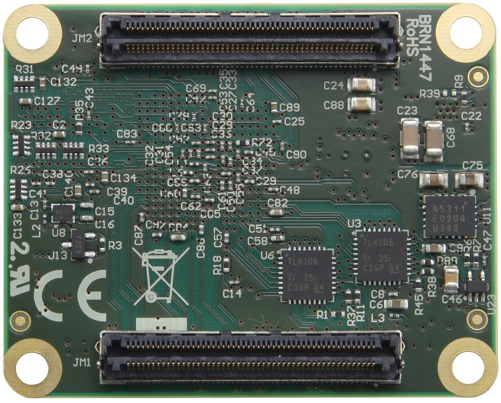 |
Top view | Bottom view |
Detailed Description
PL Programmable Logic
The TE0710 board is populated with the Artix-7 Series Families FPGA. The devices can be programmed with the free Xilinx Vivado WebPACK software. Further information on the Artix-7 FPGA can be found in the Xilinx document 7 Series FPGAs Overview (DS180).
FPGA | Logic Cells | Flip-Flops | BRAM |
XC7A15T-2CSG324C | 16,640 | 20,800 | 25 |
XC7A35T-2CSG324C | 33,280 | 41,600 | 50 |
XC7A50T-2CSG324C | 52,160 | 65,200 | 75 |
XC7A75T-2CSG324C | 75,520 | 94,400 | 105 |
XC7A100T-2CSG324C | 101,440 | 126,800 | 135 |
Configuration Modes
The following two FPGA configuration interfaces are supported:
Mode | Setting | Notes |
JTAG | JTAG | For debugging purposes |
SPI Flash | SPI Master 4-bit mode | Main configuration mode: 4-Bit mode must be used when generating bitstream |
TE0710 Configuation pin settings
Config Pin | Setting | Notes |
| M0 | 3.3V | Bootmode setting: Master SPI
|
| M1 | 0V | |
| M2 | 0V | |
| CFGBVS | 3.3V | Select 3.3V as Config Bank I/O Voltage |
| PUDC | Strong pull-up to 3.3V | Pre-configuration pull-ups are DISABLED |
Configuration Memory
TE0710 standard assembly option includes 32MByte SPI Flash for configuration and data storage. This memory is large enough to hold at least 4 uncompressed FPGA Bitstreams.
Parameter | Value | Notes |
Memory size (MBytes) | 32 |
|
Vendor | Spansion | |
Device type | S25FL256SAGBHI20 |
|
Vivado CFGMEM | s25fl256sxxxxxx0-spi-x1_x2_x4 | Value to be used with Vivado labtools flash programmer |
Vivado Board Part File Interface name | SPI Flash |
Parameter values for the SPI Flash memory included in the standard assembly option.
XADC
XADC is configured with internal reference voltage option. All XADC inputs that are shared with FPGA I/O are available in the B2B Connector. There is no access to the dedicated XADC input pins.
Clock Sources
The TE0710 board has a 3.3V single ended 100MHz oscillator (U8). It is wired to an FPGA MRCC clock input on bank 35.
Oscillator: Si Time SiT8008AI-73-XXS-100.000000E (100 MHz)
Frequency stability: 50 ppm
IC Designator | Description | Frequency | Used as | FPGA Pin | IO Standard | Vivado Board Part Interface |
U8 | MEMS Oscillator | 100 MHz | System Clock | F4 | LVCMOS15 | System Clock |
In standard assembly option MEMS oscillator with 100MHz Frequency and 50 ppm stability is used. Other frequencies possible for custom order.
Reset Sources
Reset Type | Source | Notes |
| Power On Reset | System Controller | PROG_B released after power on causing FPGA reconfiguration |
| Config Reset | JM2.18 | Active low value forces FPGA reconfiguration |
| Dummy Reset | FPGA pin D9 | Can be used as reset with fixed always inactive value if needed (may have to add pullup or pulldown constraint) |
| Soft Reset | Any FPGA B2B I/O | User defined soft reset input with user defined polarity |
| Debug Reset | Microblaze MDM | JTAG debugger soft reset |
LED's
The TE0710 board has 3 LEDs. One is user led, which is connected to Pin L15 on the Bank 14. The other two are connected to the system controller.
LED | Color | IOSTANDARD | FPGA Pin | Description |
D1 | red | N/A | N/A | System controller status LED |
D2 | green | N/A | N/A | System controller status LED |
D3 | red | LVCMOS33 | L15 | User LED, active LOW |
JTAG
JTAG access is provided to the Xilinx Artix-7 FPGA (U5) and system controller (U4) through connector JM2. Selection of JTAG is controlled by the JTAGSEL pin (JM1.89) in connector JM1.
JTAG Bus Access
| Signal | B2B Module | B2B Base | Description |
|---|---|---|---|
| TCK | JM2: 99 |
| |
| TDI | JM2: 95 | . | |
| TDO | JM2: 97 | ||
| TMS | JM2: 93 | ||
| JTAGSEL | JM1: 89 | keep low or GND for normal operation |
The use of Xilinx legacy development tools (ISE, Impact) is not recommended. Impact does recognize only A100T, any smaller Artix is not even recognized as Xilinx FPGA by Impact.
DDR3 Memory
The TE0710 board contains one DDR3 component with a capacity of 4Gb.
- Part number: MEM4G08D3EABG-125 (Memphis)
- Supply voltage: 1.5V
- Organization: 64M words x 8 bits x 8 banks
- Memory speed limited by Artix speed grade and MIG
Configuration of the DDR3 memory controller in the FPGA should be done using the Xilinx MIG tool in the Vivado IP catalog. Refer to the reference design section (DDR3 Reference Design) for information on how to do this.
DDR3 Memory Connections to the FPGA
| FPGA Pin | FPGA Bank | I/O Standard | Comment |
| A4 | 35 | DIFF_SSTL15 | DDR3 Clock |
| A3 | 35 | DIFF_SSTL15 | DDR3 Clock |
| B1 | 35 | LVCMOS15 | DDR3 Reset |
| G6 | 35 | SSTL15 | DDR3 ODT |
| H5 | 35 | SSTL15 | DDR3 CS |
| H2 | 35 | SSTL15 | DDR3 CKE |
| J2 | 35 | SSTL15 | DDR3 RAS |
| H6 | 35 | SSTL15 | DDR3 CAS |
| G4 | 35 | SSTL15 | DDR3 WE |
| D3 | 35 | SSTL15 | DDR3 Address 0 |
| B2 | 35 | SSTL15 | DDR3 Address 1 |
| G1 | 35 | SSTL15 | DDR3 Address 2 |
| D4 | 35 | SSTL15 | DDR3 Address 3 |
| E1 | 35 | SSTL15 | DDR3 Address 4 |
| D2 | 35 | SSTL15 | DDR3 Address 5 |
| F1 | 35 | SSTL15 | DDR3 Address 6 |
| D5 | 35 | SSTL15 | DDR3 Address 7 |
| C1 | 35 | SSTL15 | DDR3 Address 8 |
| B3 | 35 | SSTL15 | DDR3 Address 9 |
| E3 | 35 | SSTL15 | DDR3 Address 10 |
| A1 | 35 | SSTL15 | DDR3 Address 11 |
| E2 | 35 | SSTL15 | DDR3 Address 12 |
| B4 | 35 | SSTL15 | DDR3 Address 13 |
| C2 | 35 | SSTL15 | DDR3 Address 14 |
| H1 | 35 | SSTL15 | DDR3 Address 15 |
| J4 | 35 | SSTL15 | DDR3 Bank0 |
| F3 | 35 | SSTL15 | DDR3 Bank1 |
| G2 | 35 | SSTL15 | DDR3 Bank2 |
| C5 | 35 | SSTL15 | DDR3 Data 0 |
| B7 | 35 | SSTL15 | DDR3 Data 1 |
| B6 | 35 | SSTL15 | DDR3 Data 2 |
| C6 | 35 | SSTL15 | DDR3 Data 3 |
| C7 | 35 | SSTL15 | DDR3 Data 4 |
| D8 | 35 | SSTL15 | DDR3 Data 5 |
| E5 | 35 | SSTL15 | DDR3 Data 6 |
| E7 | 35 | SSTL15 | DDR3 Data 7 |
| A6 | 35 | DIFF_SSTL15 | DDR3 Data Strobe |
| A5 | 35 | DIFF_SSTL15 | DDR3 Data Strobe |
| E6 | 35 | SSTL15 | DDR3 Data Mask |
Ethernet PHY
The TE0710 board has two 10/100M Ethernet PHY's TLK106 connected using MII interface to FPGA bank 14.
Ethernet PHY Connections
| FPGA Pin | FPGA Bank | Net Name | I/O Standard | Comment |
| U14 | 14 | ETH-RST | LVCMOS33 | Ethernet Reset, active-low |
| T14 | 14 | ETH_TXCLK | LVCMOS33 | Ethernet transmit clock input from PHY |
| R16 | 14 | ETH_TX_D0 | LVCMOS33 | Ethernet transmit data 0. Output to Ethernet PHY. |
| U18 | 14 | ETH_TX_D1 | LVCMOS33 | Ethernet transmit data 1. Output to Ethernet PHY. |
R18 | 14 | ETH_TX_D2 | LVCMOS33 | Ethernet transmit data 2. Output to Ethernet PHY. |
| R17 | 14 | ETH_TX_D3 | LVCMOS33 | Ethernet transmit data 3. Output to Ethernet PHY. |
| R15 | 14 | ETH_TX_EN | LVCMOS33 | Ethernet transmit enable. Output to Ethernet PHY. |
| N15 | 14 | ETH_RXCLK | LVCMOS33 | Ethernet receive clock input from PHY. |
| U12 | 14 | ETH_RX_D0 | LVCMOS33 | Ethernet receive data 0. Input from Ethernet PHY. |
| V12 | 14 | ETH_RX_D1 | LVCMOS33 | Ethernet receive data 1. Input from Ethernet PHY. |
| U13 | 14 | ETH_RX_D2 | LVCMOS33 | Ethernet receive data 2. Input from Ethernet PHY. |
| T15 | 14 | ETH_RX_D3 | LVCMOS33 | Ethernet receive data 3. Input from Ethernet PHY. |
| V10 | 14 | ETH_RX_DV | LVCMOS33 | Ethernet receive data valid. Input from Ethernet PHY. |
| V11 | 14 | ETH_RX_ER | LVCMOS33 | Ethernet receive error. Input from Ethernet PHY. |
| T9 | 14 | ETH_COL | LVCMOS33 | Ethernet collision detect input from Ethernet PHY. |
| T18 | 14 | ETH_INT | LVCMOS33 | Ethernet power down or interrupt. (default function is power down) |
| V15 | 14 | LINK_LED | LVCMOS33 | Ethernet LED Pin to indicate status. Mode 1: LINK Indication LED; Mode 2: ACT Indication LED |
| T13 | 14 | MDC | LVCMOS33 | Ethernet to PHY MII Management clock |
| V14 | 14 | MDIO | LVCMOS33 | PHY MDIO data I/O ( 3-state buffer) |
| P17 | 14 | ETH2_TXCLK | LVCMOS33 | Ethernet 2 transmit clock input from PHY. |
| M13 | 14 | ETH2_TX_D0 | LVCMOS33 | Ethernet 2 transmit data 0. Output to Ethernet PHY. |
M16 | 14 | ETH2_TX_D1 | LVCMOS33 | Ethernet 2 transmit data 1. Output to Ethernet PHY. |
| M17 | 14 | ETH2_TX_D2 | LVCMOS33 | Ethernet 2 transmit data 2. Output to Ethernet PHY. |
| L16 | 14 | ETH2_TX_D3 | LVCMOS33 | Ethernet 2 transmit data 3. Output to Ethernet PHY. |
| N16 | 14 | ETH2_TX_EN | LVCMOS33 | Ethernet 2 transmit enable. Output to Ethernet PHY. |
| p15 | 14 | ETH2_RXCLK | LVCMOS33 | Ethernet 2 receive clock input from PHY. |
| V17 | 14 | ETH2_RX_D0 | LVCMOS33 | Ethernet 2 receive data 0. Input from Ethernet PHY. |
| T16 | 14 | ETH2_RX_D1 | LVCMOS33 | Ethernet 2 receive data 1. Input from Ethernet PHY. |
| U17 | 14 | ETH2_RX_D2 | LVCMOS33 | Ethernet 2 receive data 2. Input from Ethernet PHY. |
| N17 | 14 | ETH2_RX_D3 | LVCMOS33 | Ethernet 2 receive data 3. Input from Ethernet PHY. |
| R11 | 14 | ETH2_RX_DV | LVCMOS33 | Ethernet 2 receive data valid. Input from Ethernet PHY. |
| U16 | 14 | ETH2_RX_ER | LVCMOS33 | Ethernet 2 receive error. Input from Ethernet PHY. |
| P14 | 14 | ETH2_COL | LVCMOS33 | Ethernet 2 collision detect input from Ethernet PHY. |
| D10 | 16 | ETH2_INT | LVCMOS33 | Ethernet 2 power down or interrupt |
| T10 | 14 | LINK_LED2 | LVCMOS33 | Ethernet LED Pin to indicate status. Mode 1: LINK Indication LED; Mode 2: ACT Indication LED |
| N14 | 14 | MDC2 | LVCMOS33 | Ethernet 2 to PHY MII 2 Management clock |
| P18 | 14 | MDIO2 | LVCMOS33 | PHY MDIO data I/O ( 3-state buffer) |
MAC Address EEPROM
The TE0710 board has a UNI/O serial EEPROM with EUI-48™ Node Identity. This device is a 2 Kbit Serial Electrically Erasable PROM. It is organized in blocks of x8-bit memory and supports single I/O UNI/O® serial bus. It has a built-in 48-bit Extended Unique Identifier (EUI) that is needed to identify the network hardware’s physical address. These built-in MAC addresses enable designer to buy addresses only when needed, and also eliminate the need for serialization and programming. The address is also EUI-64 compatible, and it is write-protected to ensure tamper-proof designs. It contains an 8-bit instruction register and is accessed via the SCIO pin. The Address Data is embedded into the I/O stream through Manchester encoding. The bus is controlled by a master device which determines the clock period, controls the bus access and initiates all operations, while the serial EEPROM works as slave.
- Part number: 11AA02E48T-I/TT (Microchip)
- Supply voltage: 3.3V
Pre-programmed Globally Unique, 48-bit Node Address
- Compatible with EUI-48™ and EUI-64™
- 256 x 8 Bit Organization
| FPGA Pin | Bank | I/O Standard | Comment | Function |
|---|---|---|---|---|
| D9 | 16 | LVCMOS33 | Serial bit stream (SCIO) | Serial Clock, Data Input/Output |
For more information about this device, please refer to the Microchip 11AA02E48 Datasheet.
Board-to-Board Connectors
Unable to render {include} The included page could not be found.
View and download the connector pinout for this module in the master pinout table here: Master Pinout Table
Initial Delivery state
Storage device name | Content | Notes |
| SPI Flash OTP Area | Empty, not programmed | Except serial number programmed by flash vendor |
| SPI Flash Quad Enable bit | Programmed | Must be programmed for SPI Flash Boot |
| SPI Flash main array | demo design | |
| EFUSE USER | Not programmed | |
| EFUSE Security | Not programmed |
Revision History For This Product
Revision | Changes |
02 | Current Hardware Revision |
Technical Specification
Absolute Maximum Ratings
Parameter | Min | Max | Units | Notes |
Vin supply voltage | -0.3 | 6.0 | V |
|
Vin33 supply voltage | -0.4 | 3.6 | V |
|
I/O voltage on any FPGA I/O | -0.4 | Vcco+0.55 | V | |
Voltage on JTAG pins | -0.5 | 3.75 | V | When Vin33 is powered |
Storage Temperature | -40 | +100 | C |
|
Recommended Operating Conditions
| Parameter | Min | Max | Units | Notes | Reference document |
|---|---|---|---|---|---|
| Vin supply voltage | 2.4 | 5.5 | V | ||
| Vin33 supply voltage | 1 | 3.465 | V | ||
| PL IO Bank supply voltage for HR I/O banks (VCCO) | 1.14 | 3.465 | V | Xilinx document DS181 | |
| I/O input voltage for HR I/O banks | -0.20 | Vcco+0.20 | V | Xilinx document DS181 | |
| Voltage on Module JTAG pins | 3.135 | 3.465 | V | Xilinx document DS181 |
Please check Xilinx Datasheet for complete list of Absolute maximum and recommended operating ratings for the Artix-7 device (DS181).
Physical Dimensions
Module size: 50 mm × 40 mm. Please download the assembly diagram for exact numbers.
Mating height with standard connectors: 8mm
PCB thikness: 1.6mm
- Highest part on PCB: approx. 2.5mm. Please download the step model for exact numbers.
Download physical dimensions here: TE0710 Physical Dimensions
Power Supplies
Vin | 3.3 V to 5.5 V | Typical 200mA, depending on customer design and connections. |
Vin 3.3 V | 3.3 V | Typical 50mA, depending on customer design and connections. |
For startup, a power supply with minimum current capability of 2A is recommended.
Vin and Vin 3.3V can be connected to the same source (3.3 V).
Temperature Ranges
Commercial grade modules | 0 °C to +70 °C |
Industrial grade modules | -40 °C to +85 °C |
Depending on the customer design, additional cooling might be required.
Weight
| Weight | Note |
|---|---|
11.5 g | without bolts |
20.3 g | with bolts |
Downloads For This Product
Recommended Software: Xilinx Vivado WebPACK (free license)
A15T, A35T, A50T, A75T are not supported by Xilinx legacy tools (ISE, Impact).
The schematic is available for download here: TE0710 Schematic
Resources
Document Change History
| Date | Revision | Authors | Description |
|---|---|---|---|
| 2016-01-18 | |||
| 2015-12-15 | 0.1
| Antti Lukats | |
| All | Antti Lukats |
Disclaimer
Data Privacy
Please also note our data protection declaration at https://www.trenz-electronic.de/en/Data-protection-Privacy
Document Warranty
The material contained in this document is provided “as is” and is subject to being changed at any time without notice. Trenz Electronic does not warrant the accuracy and completeness of the materials in this document. Further, to the maximum extent permitted by applicable law, Trenz Electronic disclaims all warranties, either express or implied, with regard to this document and any information contained herein, including but not limited to the implied warranties of merchantability, fitness for a particular purpose or non infringement of intellectual property. Trenz Electronic shall not be liable for errors or for incidental or consequential damages in connection with the furnishing, use, or performance of this document or of any information contained herein.
Limitation of Liability
In no event will Trenz Electronic, its suppliers, or other third parties mentioned in this document be liable for any damages whatsoever (including, without limitation, those resulting from lost profits, lost data or business interruption) arising out of the use, inability to use, or the results of use of this document, any documents linked to this document, or the materials or information contained at any or all such documents. If your use of the materials or information from this document results in the need for servicing, repair or correction of equipment or data, you assume all costs thereof.
Copyright Notice
No part of this manual may be reproduced in any form or by any means (including electronic storage and retrieval or translation into a foreign language) without prior agreement and written consent from Trenz Electronic.
Technology Licenses
The hardware / firmware / software described in this document are furnished under a license and may be used /modified / copied only in accordance with the terms of such license.
Environmental Protection
To confront directly with the responsibility toward the environment, the global community and eventually also oneself. Such a resolution should be integral part not only of everybody's life. Also enterprises shall be conscious of their social responsibility and contribute to the preservation of our common living space. That is why Trenz Electronic invests in the protection of our Environment.
REACH, RoHS and WEEE
REACH
Trenz Electronic is a manufacturer and a distributor of electronic products. It is therefore a so called downstream user in the sense of REACH. The products we supply to you are solely non-chemical products (goods). Moreover and under normal and reasonably foreseeable circumstances of application, the goods supplied to you shall not release any substance. For that, Trenz Electronic is obliged to neither register nor to provide safety data sheet. According to present knowledge and to best of our knowledge, no SVHC (Substances of Very High Concern) on the Candidate List are contained in our products. Furthermore, we will immediately and unsolicited inform our customers in compliance with REACH - Article 33 if any substance present in our goods (above a concentration of 0,1 % weight by weight) will be classified as SVHC by the European Chemicals Agency (ECHA).
RoHS
Trenz Electronic GmbH herewith declares that all its products are developed, manufactured and distributed RoHS compliant.
WEEE
Information for users within the European Union in accordance with Directive 2002/96/EC of the European Parliament and of the Council of 27 January 2003 on waste electrical and electronic equipment (WEEE).
Users of electrical and electronic equipment in private households are required not to dispose of waste electrical and electronic equipment as unsorted municipal waste and to collect such waste electrical and electronic equipment separately. By the 13 August 2005, Member States shall have ensured that systems are set up allowing final holders and distributors to return waste electrical and electronic equipment at least free of charge. Member States shall ensure the availability and accessibility of the necessary collection facilities. Separate collection is the precondition to ensure specific treatment and recycling of waste electrical and electronic equipment and is necessary to achieve the chosen level of protection of human health and the environment in the European Union. Consumers have to actively contribute to the success of such collection and the return of waste electrical and electronic equipment. Presence of hazardous substances in electrical and electronic equipment results in potential effects on the environment and human health. The symbol consisting of the crossed-out wheeled bin indicates separate collection for waste electrical and electronic equipment.
Trenz Electronic is registered under WEEE-Reg.-Nr. DE97922676.
Overview
Content Tools