Table of Contents
Overview
The Trenz Electronic TEM0002-01 SmartBerry with Raspberry Pi form factor, is an industrial-grade module based on Microsemi SmartFusion2 SoC (System on a Chip). The Module has 128MB DDR3 SDRAM, a Gigabit Ethernet PHY, four Pmods, a GPIO Pin header compatible to the Raspberry Pi pinout and a Micro USB to UART interface. SmartFusion2 combines a 166 MHz Cortex-M3 core with 256 KByte Flash, 80 KByte SRAM and a 12 kLUT FPGA core logic.
Key Features
- Microsemi SmartFusion2 SoC FPGA (M2S010)
- 128 MByte DDR3 SDRAM
- On board power converters for all needed voltages
- 40 pin header (compatible to Raspberry Pi pinout)
- 4 x 12 pin Pmods
- Gigabit Ethernet PHY with RGMII interface
- JTAG and UART via Micro USB
- 3 pin header for Live Probes
- 2 x User Button
- 2 x status LED
1 x RGB LED
Additional assembly options are available for cost or performance optimization upon request.
Block Diagram
Figure 1: TEM0002-01 block diagram.
Main Components
Figure 2: TEM0002-01 main components.
- Microsemi SmartFusion2 SoC FPGA, U2
- USB to UART/FIFO (FTDI FT2232H), U3
- Gigabit ETH connector, J2
- 4x 2x6 pin Pmod, P1, P2, P3, P4
- GPIO pin header compatible to Raspberry Pi, J8
- Micro USB 2.0, J1
- EEPROM 4KBIT (M93C66-R), U6
- 2x User Button, S4, S5
- RGB LED, D3
- LED red, D1 and green, D2
- Live Probe pins, J4
- Reset jumper, J13
- JTAG select jumper, J6
- Board power header, J5
- 1Gb DDR3/L SDRAM, U5
- MicroSD memory card connector, J3
- Gigabit Ethernet PHY, U1
Initial Delivery State
Storage device name | Content | Notes |
|---|---|---|
| Microsemi SmartFusion2 SoC FPGA, U2 | Demo Design | - |
| EEPROM, U6 | Programmed | FTDI (FT2232H) configuration data. |
Table 1: Initial delivery state of programmable devices on the module.
Boot Process
The SmartBerry supports configuration of the system via JTAG by the FTDI USB bridge.
Signals, Interfaces and Pins
I/Os
26 I/O signals provided on the Rasperry Pi compatible header are connected to banks with 3.3V. Dpending on the configuration of the SoC, also GPIOs of the Microprocessor subsystem can be routet to the SoC Pins.
| FPGA SoC Signal | SOC Pin | Header Pin | Raspberry Pi Signal |
|---|---|---|---|
| MSIO19PB2 | U2-H16 | 3 | GPIO2 |
| MSIO16PB2 | U2-J17 | 5 | GPIO3 |
| MSIO2PB2 | U2-T18 | 7 | GPIO4 |
| MSIO1PB2 | U2-U18 | 8 | GPIO14 |
| MSIO5NB2 | U2-R18 | 10 | GPIO15 |
| MSIO11NB2 | U2-M17 | 11 | GPIO17 |
| MSIO6PB2 | U2-P18 | 12 | GPIO18 |
| MSIO14PB2 | U2-L15 | 13 | GPIO27 |
| MSIO17PB2 | U2-K16 | 15 | GPIO22 |
| MSIO11PB2 | U2-N16 | 16 | GPIO23 |
| MSIO27NB1 | U2-B19 | 18 | GPIO24 |
| MSIO25NB1 | U2-C20 | 19 | GPIO10 |
| MSIO25PB1 | U2-D20 | 21 | GPIO9 |
| MSIO22NB1 | U2-F18 | 22 | GPIO25 |
| MSIO20NB2 | U2-F20 | 23 | GPIO11 |
| MSIO20PB2 | U2-G19 | 24 | GPIO08 |
| MSIO18PB2 | U2-H19 | 26 | GPIO07 |
| MSIO28PB1 | U2-A20 | 27 | ID_SDA |
| MSIO28NB1 | U2-A19 | 28 | ID_SCL |
| MSIO16NB2 | U2-J18 | 29 | GPIO05 |
| MSIO15NB2 | U2-J20 | 31 | GPIO06 |
| MSIO15PB2 | U2-K20 | 32 | GPIO12 |
| MSIO14NB2 | U2-L16 | 33 | GPIO13 |
| MSIO13NB2 | U2-L19 | 35 | GPIO19 |
| MSIO13PB2 | U2-L20 | 36 | GPIO16 |
| MSIO8PB2 | U2-N20 | 37 | GPIO26 |
| MSIO8NB2 | U2-M19 | 38 | GPIO20 |
| MSIO4NB2 | U2-N19 | 40 | GPIO21 |
Table 2: General overview of I/O signals connected to the SoC.
Further I/Os are provided via the Pmod connectors descriebed below.
Pmods
The module provides four 2x6 female Pmod connectors. Two of the headers (P2 and P3) are arranged to use as dual 12 pin Pmod. According to the standard on all four headers Pin 5 and 11 are connected to ground, 6 and 12 to 3.3V.
| FPGA SoC Signal | Pin | Pmod Signal | Pmod Pin |
|---|---|---|---|
| MSIO71PB7 | U2-F3 | PB-01 | P1-1 |
| MSIO71NB7 | U2-F4 | PB-02 | P1-2 |
| MSIO68NB7 | U2-E3 | PB-03 | P1-3 |
| MSIO80NB7 | U2-H4 | PB-04 | P1-4 |
| MSIO75PB7 | U2-G4 | PB-05 | P1-7 |
| MSIO75NB7 | U2-F5 | PB-06 | P1-8 |
| MSIO67NB7 | U2-E5 | PB-07 | P1-9 |
| MSIO78NB7 | U2-G3 | PB-08 | P1-10 |
| MSIO79PB7 | U2-G1 | PC-01 | P2-1 |
| MSIO79NB7 | U2-F1 | PC-02 | P2-2 |
| MSIO70NB7 | U2-E2 | PC-03 | P2-3 |
| MSIO64PB7 | U2-C1 | PC-04 | P2-4 |
| MSIO78PB7 | U2-G2 | PC-05 | P2-7 |
| MSIO70PB7 | U2-E1 | PC-06 | P2-8 |
| MSIO68PB7 | U2-D2 | PC-07 | P2-9 |
| MSIO64NB7 | U2-C2 | PC-08 | P2-10 |
| MSIO117NB4 | U2-Y16 | PA-01 | P3-1 |
| MSIO117PB4 | U2-Y15 | PA-02 | P3-2 |
| MSIO112PB4 | U2-W13 | PA-03 | P3-3 |
| MSIO110PB4 | U2-V12 | PA-04 | P3-4 |
| MSIO118PB4 | U2-W15 | PA-05 | P3-7 |
| MSIO112NB4 | U2-W14 | PA-06 | P3-8 |
| MSIO105NB4 | U2-Y13 | PA-07 | P3-9 |
| MSIO104PB4 | U2-V11 | PA-08 | P3-10 |
| MSIO4PB2 | U2-P20 | PD-01 | P4-1 |
| MSIO3NB2 | U2-R20 | PD-02 | P4-2 |
| MSIO2NB2 | U2-T19 | PD-03 | P4-3 |
| MSIO0PB2 | U2-V20 | PD-04 | P4-4 |
| MSIO6NB2 | U2-P19 | PD-05 | P4-7 |
| MSIO3PB2 | U2-T20 | PD-06 | P4-8 |
| MSIO1NB2 | U2-U19 | PD-07 | P4-9 |
| MSIO0NB2 | U2-V19 | PD-08 | P4-10 |
Table 3: Overview of Pmod signals connected to the SoC.
JTAG Interface
JTAG access to the SoC components is provided through the micro usb connector via the FTDI usb to UART bridge. Depending on the jumper J6 the JTAGSEL signal SW3 switches the JTAG interface to either the FPGA fabric TAP (OPEN, high) or the Cortex-M3 JTAG debug interface (CLOSED, low). JTAG signals are powered by 3.3V.
FTDI signal | pin | JTAG Signal | Microsemi SmartFusion2 SoC pin |
|---|---|---|---|
| ADBUS0 | U3-12 | TCK | U2-W19 |
| ADBUS1 | U3-13 | TDI | U2-V16 |
| ADBUS2 | U3-14 | TDO | U2-Y20 |
| ADBUS3 | U3-15 | TMS | U2-V17 |
Table 4: JTAG interface signals.
SD Card Interface
The SD Card interface is connected to bank 2 of the SoC
| FPGA / SoC Pin | Connected To | Signal Name | Notes |
|---|---|---|---|
| U2-H16 | J3-9 | SD_CD | Card detect switch |
| U2-N15 | J3-7 | SD_D0 | |
| U2-G18 | J3-8 | SD_D1 | |
| U2-R16 | J3-1 | SD_D2 | |
| U2-R17 | J3-2 | SD_D3 | |
| U2-R15 | J3-3 | SD_CMD | |
| U2-P15 | J3-5 | SD_CLK |
Table 5: SD Card interface signals and connections.
Ethernet Interface
| PHY Pin | Signal | Microsemi SmartFusion2 SoC signal | Pin | Notes |
|---|---|---|---|---|
| U1-25 | ETH_TXCK | MSIOD84PB6 | U2-K7 | |
| U1-23 | ETH_TXCTL | MSIOD87NB6 | U2-K3 | |
| U1-26 | ETH_TXD0 | MSIOD93PB6 | U2-L1 | |
| U1-28 | ETH_TXD1 | MSIOD97NB6 | U2-M2 | |
| U1-29 | ETH_TXD2 | MSIOD97PB6 | U2-M1 | |
| U1-30 | ETH_TXD3 | MSIOD95PB6 | U2-M3 | |
| U1-22 | ETH_RRXCK | MSIOD84PB6 | U2-J2 | |
| U1-21 | ETH_RRXCTL | MSIOD93NB6 | U2-K1 | |
| U1-20 | ETH_RRXD0 | MSIOD86PB6 | U2-K5 | |
U1-18 | ETH_RRXD1 | MSIOD82PB6 | U2-H1 | |
| U1-17 | ETH_RRXD2 | MSIOD82NB6 | U2-H2 | |
| U1-16 | ETH_RRXD3 | MSIOD83PB6 | U2-J4 | |
| U1-31 | ETH_MDC | MSIOD99PB6 | U2-N1 | |
| U1-33 | ETH_MDIO | MSIOD99NB6 | U2-N2 | |
| U1-34 | ETH_MDINT | MSIOD98PB6 | U2-N4 | |
| U1-35 | ETH_RST | MSIO114PB4 | U2-R13 | |
| U1-36 | PHY_RCLKOUT | MSIO102NB4/CCC_NE1_CLKIO | U2-W10 | |
| U1-39 | PHY_LED0 | MSIO104NB4 | U2-U11 | |
| U1-38 | PHY_LED1 | MSIO116PB4 | U2_T14 |
Table 6: Ethernet PHY signals and connections.
I2C Interface
There are no on-board I2C devices. For Raspberry Pi compability the device detection I2C bus is routed from the header J8-27/28 to Bank 1 U2-A20/A19 (SDA/SCL).
| I2C Device | I2C Address | Notes |
|---|---|---|
| Header J8 | 0x50 | Device detection/identification. |
Table 7: I2C slave device addresses.
On-board Peripherals
DDR Memory
TEM0002 has 1Gb industrial grade DDR3 SDRAM (U5). A 16-bit wide memory bus providing total of 128 MBytes of on-board RAM. Specification is 800 MHz clocking resulting in 1600 Mb/s data rate and timings of 11-11-11 (CL-TRCD-TRP).
Gigabit Ethernet PHY
On-board Gigabit Ethernet PHY (J2) is provided by Microsemi VSC8531 chip (U1). The Ethernet PHY RGMII interface is connected to bank 6 of the Microsemi SOC. I/O voltage is fixed at 1.5V. The reference clock input of the PHY is supplied from an external 25.000000 MHz oscillator (U11).
Oscillators
The module has following reference clock signals provided by on-board oscillators:
| Clock Source | Schematic Name | Frequency | Clock Destination |
|---|---|---|---|
| Crystal CX3225CA25000D0HSSCC | Y1 | 25.000 MHz1 | SmartFusion2 SoC U2 Main XTAL |
| Crystal ECX-31B | Y2 | 32.768 KHz | SmartFusion2 SoC U2 AUX XTAL |
| SiTime SiT8008AI oscillator | U11 | 25.000000 MHz | Gb Ethernet Copper PHY U1A |
| SiTime SiT8008AI oscillator | U14 | 25.000000 MHz | SmartFusion2 SoC U2-Y12 Bank 4 |
Table 8: Reference clock signals.
1In REV02, Y1 will be replaced by a 12 MHz crystal.
On-board LEDs
| LED | Color | Connected to | SoC FPGA Signal | Description and Notes |
|---|---|---|---|---|
| D1 | Red | U2-G16 Bank 1 | MSIO21PB1 | |
| D2 | Green | U2-G17 Bank 1 | MSIO21NB1 | |
| D3 | RGB | U2-H5 Bank 7, U2-F6 Bank 7, U2-H6 Bank 7 | MSIO80PB7, MSIO67PB7, MSIO81NB7 | |
| J2 | Green, Yellow | U2-Y10 Bank 4, U2-U12 Bank 4 | MSIO102PB4, MSIO110NB4 | Ethernet: LED1A, LED1B |
| J2 | Green, Yellow | U2-V14 Bank 4, U2-U14 Bank 4 | MSIO115PB4, MSIO115PB4 | Ethernet: LED2A, LED2B |
Table 9: On-board LEDs.
On-board Buttons
| Button | Connected to | SoC FPGA Signal |
|---|---|---|
| S4 | U2-E17 Bank 1 | MSIO24PB1 |
| S5 | U2-E16 Bank 1 | MSIO24NB1 |
Table 10: On-board Buttons.
Power and Power-On Sequence
There is no specific power on Sequence. Just supply with 5V via the micro USB J1 or the J5 PWR_IN with current rating sufficient for your Design.
Power Consumption
The maximum power consumption of a module mainly depends on the design running on the FPGA.
| Power Input | Typical Current |
|---|---|
| VIN | TBD* |
| 3.3VIN | TBD* |
Table 11: Typical power consumption.
* TBD - To Be Determined soon with reference design setup.
Power supply with minimum current capability of ...A for system startup is recommended.
For the lowest power consumption and highest efficiency of the on-board DC-DC regulators it is recommended to power the module from one single 3.3V supply. All input power supplies have a nominal value of 3.3V. Although the input power supplies can be powered up in any order, it is recommended to power them up simultaneously.
Power Distribution Dependencies
Figure 3: Module power distribution diagram.
Power Rails
Power Rail Name | Connector pin | Direction | Notes |
|---|---|---|---|
| VIN | J5-1 | Input | Main supply voltage. |
| 5V | J8-2, J8-4 | Output | |
| 3.3V | J8-1, J8-17 | Output | |
| 1.5V | - | Output | |
1.2V | - | Output | |
| GND | J5-2, J8-9/25/39/6/14/20/30/34 |
Table 12: Module power rails.
Bank Voltages
Bank | Schematic Name | Voltage | Voltage Range |
|---|---|---|---|
| 0 (DDR3) | 1.5V | 1.5V | - |
| 1 | 3.3V | 3.3V | - |
| 2 | 3.3V | 3.3V | - |
| 3 | 3.3V | 3.3V | - |
| 4 | 3.3V | 3.3V | - |
| 5 | 1.5V | 1.5V | - |
| 6 | 1.5V | 1.5V | - |
| 7 | 3.3V | 3.3V | - |
Table 13: I/O bank voltages.
Variants Currently In Production
| Module Variant | FPGA / SoC | Operating Temperature | Temperature Range |
|---|---|---|---|
| TEM0002-01 | M2S010 | 0°C to +70°C | commercial |
Table 14: Module variants.
Technical Specifications
Absolute Maximum Ratings
Parameter | Min | Max | Units | Reference Document |
|---|---|---|---|---|
VIN supply voltage | -0.3 | 6.0 | V | - |
Storage temperature1 | -25 | 70 | °C | - |
Table 15: Module absolute maximum ratings.
1Boundary determined by the specification of the buttons, all other components have at least a range of -40°C to 85°C.
Recommended Operating Conditions
| Parameter | Min | Max | Units | Reference Document |
|---|---|---|---|---|
| VIN supply voltage | 2.4 | 5.5 | V | - |
| Operating temperature1 | 0 | 70 | °C | - |
Table 16: Module recommended operating conditions.
1Upper bound is determined by the buttons, all other components have at least a upper bound of 85 °C.
Operating Temperature Ranges
Module operating temperature range depends also on customer design and cooling solution. Please contact us for options.
Physical Dimensions
Module size: 85 mm × 56 mm. Please download the assembly diagram for exact numbers.
PCB thickness: 1.55 mm.
Highest part on PCB: top approx. 13.3 mm (Ethernet), bottom 1.57mm (SD-Card)Please download the step model for exact numbers.
All dimensions are given in millimeters.
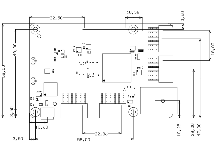
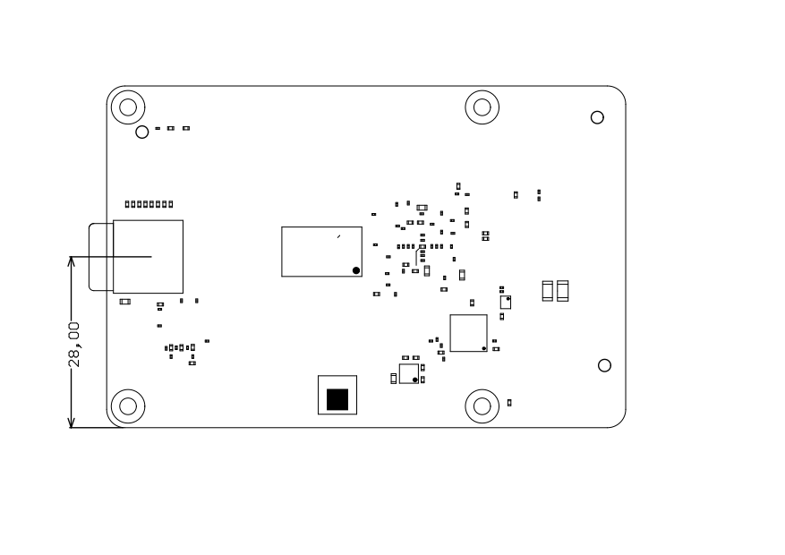
Figure 4: Module physical dimensions drawing.
Revision History
Hardware Revision History
| Date | Revision | Notes | PCN | Documentation Link |
|---|---|---|---|---|
| - | 01 | Prototypes |
Table 17: Module hardware revision history.
Hardware revision number can be found on the PCB board together with the module model number separated by the dash.
Figure 5: Module hardware revision number.
Document Change History
Date | Revision | Contributors | Description |
|---|---|---|---|
| |||
all | Jan Kumann, John Hartfiel |
Table 18: Document change history.
Disclaimer
Data Privacy
Please also note our data protection declaration at https://www.trenz-electronic.de/en/Data-protection-Privacy
Document Warranty
The material contained in this document is provided “as is” and is subject to being changed at any time without notice. Trenz Electronic does not warrant the accuracy and completeness of the materials in this document. Further, to the maximum extent permitted by applicable law, Trenz Electronic disclaims all warranties, either express or implied, with regard to this document and any information contained herein, including but not limited to the implied warranties of merchantability, fitness for a particular purpose or non infringement of intellectual property. Trenz Electronic shall not be liable for errors or for incidental or consequential damages in connection with the furnishing, use, or performance of this document or of any information contained herein.
Limitation of Liability
In no event will Trenz Electronic, its suppliers, or other third parties mentioned in this document be liable for any damages whatsoever (including, without limitation, those resulting from lost profits, lost data or business interruption) arising out of the use, inability to use, or the results of use of this document, any documents linked to this document, or the materials or information contained at any or all such documents. If your use of the materials or information from this document results in the need for servicing, repair or correction of equipment or data, you assume all costs thereof.
Product Disclaimer
Products (incl. Software and Firmware) are exclusively designed, manufactured, and distributed for industrial applications. They are not intended, authorized, or certified for use in critical safety applications, medical devices, aerospace, nuclear, life-support, traffic-control, military, or other environments where malfunction or failure could result in personal injury, death, or significant property or environmental damage.
Trenz Electronic GmbH (“Manufacturer”) excludes any liability for inappropriate use in such contexts. The Customer bears all responsibility for verifying suitability and compliance with applicable regulations when deploying in any critical-use scenario. The Customer also agrees to indemnify and hold harmless the Manufacturer from any third-party claims or liabilities arising from such use.
Copyright Notice
No part of this manual may be reproduced in any form or by any means (including electronic storage and retrieval or translation into a foreign language) without prior agreement and written consent from Trenz Electronic.
Technology Licenses
The hardware / firmware / software described in this document are furnished under a license and may be used /modified / copied only in accordance with the terms of such license.
Environmental Protection
To confront directly with the responsibility toward the environment, the global community and eventually also oneself. Such a resolution should be integral part not only of everybody's life. Also enterprises shall be conscious of their social responsibility and contribute to the preservation of our common living space. That is why Trenz Electronic invests in the protection of our Environment.
REACH, RoHS and WEEE
REACH
Trenz Electronic is a manufacturer and a distributor of electronic products. It is therefore a so called downstream user in the sense of REACH. The products we supply to you are solely non-chemical products (goods). Moreover and under normal and reasonably foreseeable circumstances of application, the goods supplied to you shall not release any substance. For that, Trenz Electronic is obliged to neither register nor to provide safety data sheet. According to present knowledge and to best of our knowledge, no SVHC (Substances of Very High Concern) on the Candidate List are contained in our products. Furthermore, we will immediately and unsolicited inform our customers in compliance with REACH - Article 33 if any substance present in our goods (above a concentration of 0,1 % weight by weight) will be classified as SVHC by the European Chemicals Agency (ECHA).
RoHS
Trenz Electronic GmbH herewith declares that all its products are developed, manufactured and distributed RoHS compliant.
WEEE
Information for users within the European Union in accordance with Directive 2002/96/EC of the European Parliament and of the Council of 27 January 2003 on waste electrical and electronic equipment (WEEE).
Users of electrical and electronic equipment in private households are required not to dispose of waste electrical and electronic equipment as unsorted municipal waste and to collect such waste electrical and electronic equipment separately. By the 13 August 2005, Member States shall have ensured that systems are set up allowing final holders and distributors to return waste electrical and electronic equipment at least free of charge. Member States shall ensure the availability and accessibility of the necessary collection facilities. Separate collection is the precondition to ensure specific treatment and recycling of waste electrical and electronic equipment and is necessary to achieve the chosen level of protection of human health and the environment in the European Union. Consumers have to actively contribute to the success of such collection and the return of waste electrical and electronic equipment. Presence of hazardous substances in electrical and electronic equipment results in potential effects on the environment and human health. The symbol consisting of the crossed-out wheeled bin indicates separate collection for waste electrical and electronic equipment.
Trenz Electronic is registered under WEEE-Reg.-Nr. DE97922676.
Overview
Content Tools