NetFPGA SUME - a Xilinx Virtex 7 FPGA board for high performance computing and networking systems
Introduction
The NetFPGA project is a group to develop open source hardware and software for rapid prototyping of high-speed, hardware-accelerated networking systems. The NetFPGA project is enabled by Field Programmable Gate Array (FPGA) technology so that users can process packets at line-rate.
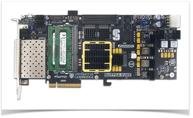
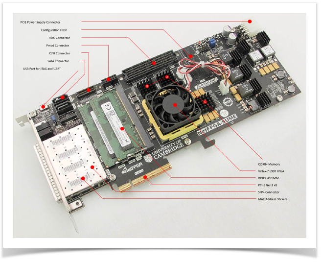
The NetFPGA-SUME board is suitable for high-performance computing and high density networking design. It is powered by Xilinx Virtex-7 690T and is co-developed by Digilent, Xilinx, the University of Cambridge, and Stanford University. The board has been used in academic and industrial researches including networks security, software defined networking, high-performance network systems.
This getting started guide covers system requirements, infrastructure, hardware test, reference designs and first reference switch project.
System Requirements
1. Operating Systems
a. You can use any operating system that is supported by Xilinx Vivado Design Suite
b. The NetFPGA team develops strictly on Linux, so the software components are developed for Linux. We recommend users to have Ubuntu 16.04.
2. CAD tools / IDE
a. Xilinx Vivado Design Suite is required. The recommend version is Xilinx Vivado 2016.4.
b. A valid license for Xilinx 10G MAC.
3. Network cables
The NetFPGA-SUME board has four SFP+ connectors for 10G Ethernet. AVAGO AFBR-709SMZ transceivers with Multimode OM3 10Gb Fibre is recommended
4. Host Motherboard:
You can use the NetPFGA-SUME board both standalone and inside a host.
a. Standalone: You need a micro-USB cable for JTAG chain and serial communication.
b. Host: The motherboard must to support PCI Express Gen3 x8. You can the detailed information at https://github.com/NetFPGA/NetFPGA-SUME-public/wiki/Motherboard-Information.
Infrastructure
NetFPGA-SUME kit includes
NetFPGA-SUME board
A micro-USB cable
4 unique MAC address stickers (one per 10G SFP+ Ethernet port)
The NetFGPA support package has:
Reusable Verilog modules (IP Cores)
Verification Infrastructure
Simulate designs (from AXI interface)
Run tests against hardware
Test data generation libraries
Build using xSim and Scapy
Use Python scripts for stimuli construction and verification
Build Infrastructure
Bitstream generation using Xilinx tools
Register system that generates addresses for all the registers and memories in a project. Uses python and tcl scripts to generate HDL code and header files.
Utilities
Register I/O
Software libraries
Hardware test
NetFPGA group has created a few hardware test so that the user can verify the hardware out of the box.
Reference Designs
The NetFPGA community offers a range of open source projects or reference designs. All can be directly downloaded from the git repository. To have access to reference designs, you must successfully register at http://netfpga.org/site/#/SUME_reg_form/. All projects implement basic functionalities of a switch, router and network interface controller (NIC) and can be uploaded on the board.
Typically, a project or reference design consists of:
HDL sources (Verilog/VHDL)
Simulation tests
Hardware tests
Optional software
First Reference Switch Project
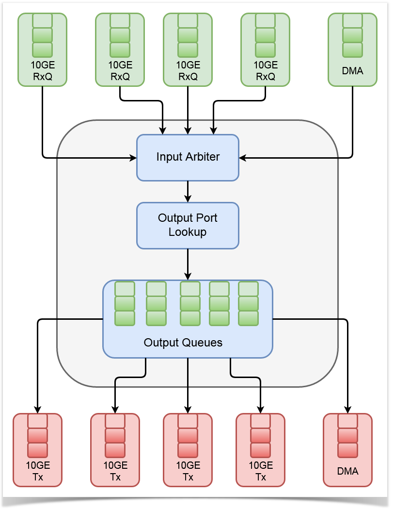
Some useful reference designs include reference NIC, reference router, reference switch and reference switch lite. For example, NetSUME-FPGA will act as a learning switch if the reference switch project is loaded on the board. The incoming packets will be transmitted to the corresponding output ports, based on MAC address. Figure 1 shows the internal structure.
Figure 1
The switching process can be broken down into five stages:
1. Input port (Rx Queues)
2. Input arbitration
3. Forwarding decision and packet modification
4. Output queueing
5. Output port
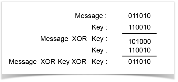
After the user understand the basic concept and underlying principle, they can modify the switch to encrypt the received data using one time pad method: make a XOR between the Message and a key K.
User can implement a Verilog module that makes the encryption and decryption of the payload. It was designed as a finite state machine (three states) to detect the header, which remains as it is, and the payload. This module was packaged as an IP and will be introduced in the switch pipeline. There are two ways to integrate the obtained IP into the main project. The block diagram (block design) is for someone who is familiar with Vivado block design. The Tcl script is good for version control or letting user understand Vivado GUI.
Use Vivado GUI and block diagram.
Use the Tcl scripts that were developed by NetFPGA community
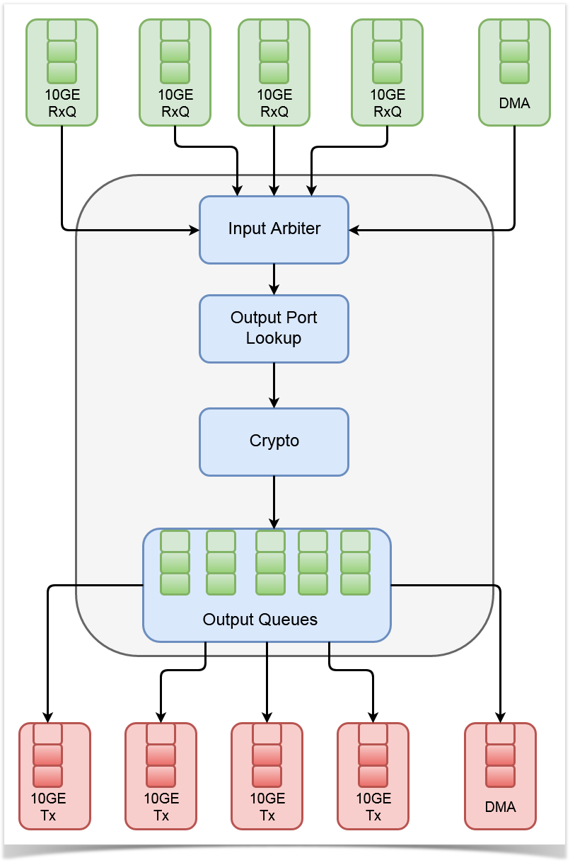
After the encryption, Figure 2 shows the modified structure called Crypo-Switch.
Figure 2
Now, user can run the simulation and debug the design. The simulation allows user to test the design without requiring lengthy synthesis process. Because the NetSUME-FPGA board has a complex FPGA architecture, the bitstream generation process takes more than 45 minutes. The simulation will be run in Vivado Simulator. To generate Ethernet packets, we used Scapy. The details is at https://github.com/NetFPGA/NetFPGA-SUME-public/wiki/NetFPGA-SUME-Simulations .
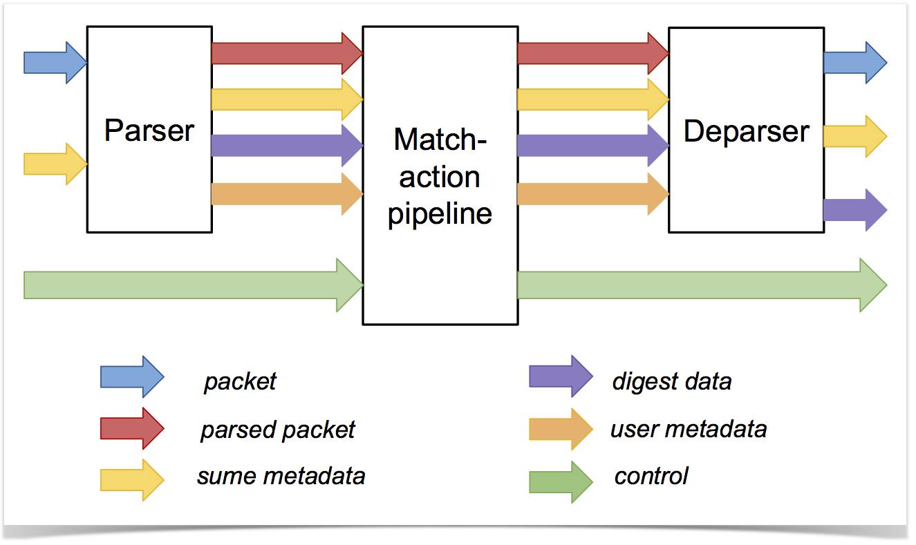
Once the user validate the design through simulation, they can generate the bitstream and upload it on the board. This approach is suitable for digital designers who know Verilog or VHDL and aim a high-performance system. For a software engineer or someone who want to parse the incoming data and take action based on the packet header or payload, they should use P4. P4 is a high level programming language that is used to describe packet processing logic and to implement forwarding-plane of network elements. Users can describe the logic in P4 and use Xilinx SDNet. The code can be compiled under Xilinx SDNet and the complied design can be uploaded in NetSUME-FPGA. There is a simple switch example based for NetFGPA SUME in Xilinx SDNet (/opt/Xilinx/SDNet/<version_number>/data/p4include/sume_switch.p4). Figure 3 shows the switch architecture.
Figure 3
References
NetFPGA Summer School courses: https://www.cl.cam.ac.uk/research/srg/netos/projects/netfpga/workshop/summer-school-2017/
NetFPGA Wiki: https://github.com/NetFPGA/NetFPGA-SUME-public/wiki

