The module can be powered by B2B connector J5 or the USB connector. If both power supplies are available, the B2B connector power supply takes precedence, disabling the USB power supply automatically.
On Board Power Rails
On-board voltage regulators provide the following power supply rails needed by the components on the module:
- 1.2V, 4.0 A max (3.0 A max REV00)
- 2.5V, 0.8 A max
- 3.3V, 3.0 A max (1.5 A max REV01)
- 1.5V, 3.0 A max (1.5 A max REV01)
The figure below show power supply diagram.
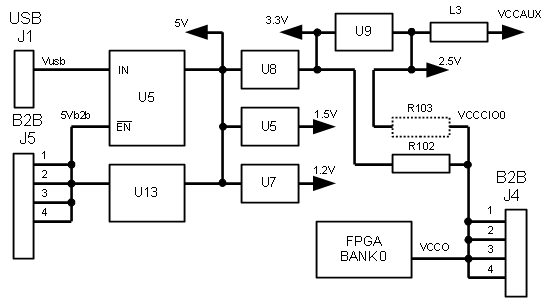
TE0630 Power diagram
The power rails are available for the FPGA and can be shared with a carrier board by the corresponding lines of the B2B connectors J4 and J5.
Please note that the power consumption of the FPGA is highly dependent on the design actually loaded. So please use a tool like Xilinx Xpower to estimate the expected power consumption of your design.
Even if the provided voltages of the module are not used on the carrier board, it is recommended to bypass them to ground with 10 nF - 100 nF capacitors.
- the module is equipped with an USB connector,
- the module is connected to a USB bus,
- no power supply is provided by B2B connectors.
In this case, other components (e.g. extension or carrier boards) may also be powered by the corresponding 5 volt line (5V) of B2B connector J5.
FPGA I/O banks power supply
Spartan-6 architecture organizes I/Os into four I/O banks, see the table below for supply voltage used for each bank.
Bank | Supply |
|---|---|
B0 | VCCIO0 |
B1 | 1.5V |
B2 | 3.3V |
B3 | 3.3V |
FPGA banks VCCIO power supply
VCCIO0 voltage can be configured in 3 ways:
- 2.5V - When resistor R103 is populated and resistor R102 is not populated.
- 3.3V - When R103 is not populated and resistor R102 is populated.
- 1.2 V ÷ 3.3 V (External supply) - When R103 is not populated and R102 is not populated. In this case external supply source have to be connected to pins 1, 2, 3, 4 of J4 B2B connector(1).
(1) See Spartan-6 documentation fo VCCIO power range.
Others options of VCCIO0 power supply are not supported and can damage the FPGA!
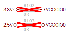
Example of VCCIO0 assembly not dependent on 2.5V power rail. The other way is also possible.
See the figure below to locate R102 and R103 on PCB.
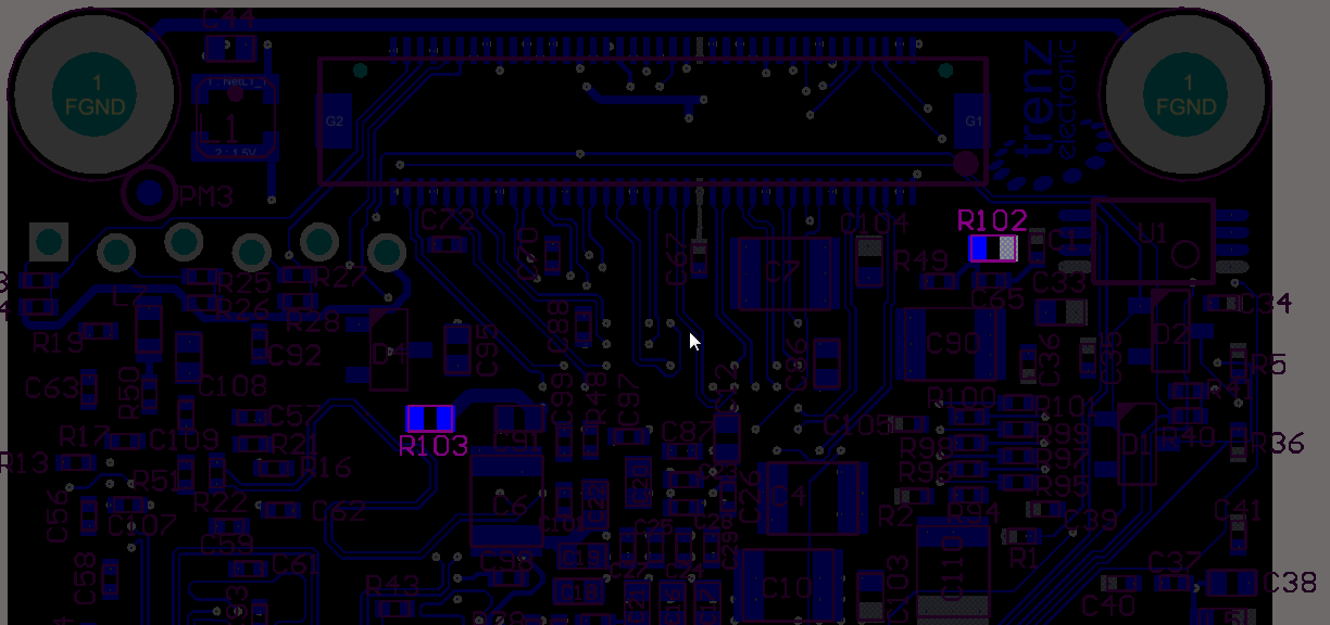
R102 and R103 location
Note that some of Spartan-6 I/O types are partially compatible, so pins of compatible types can be used as inputs for signal of other type. See "Spartan-6 FPGA SelectIO Resources" page 38 for detailed information.
During power-on, the /RESET line is first asserted. Thereafter, the supply voltage supervisor monitors the power supply rail 3.3V and keeps the /RESET line active (low) as long as the supply rail remains below the threshold voltage(2.93 volt). An internal timer delays the return of the /RESET line to the inactive state (high) to ensure proper system reset prior to a regular system start-up. The typical delay time td of 200 ms starts after the supply rail has risen above the threshold voltage.
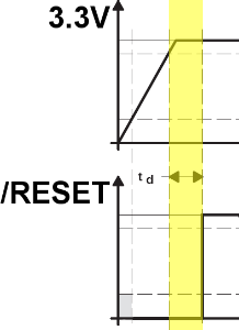
Reset on power-on
After this delay, the /RESET line is reset (high) and the FPGA configuration can start. When the supply rail voltage drops below the threshold voltage, the /RESET line becomes active (low) again and stays active (low) as long as the rail voltage remains below the threshold voltage (2.93 volt). Once the rail voltage raises again and remains over the threshold voltage for more than the typical delay time td of 200 ms, the /RESET line returns to the inactive state (high) to allow a new system start-up.
Overview
Content Tools