Host Computer's Software Connection (with SPI Flash) Available
host computer's software with FPGA through SPI are currently not availble; the connection can be only established only indirectly and for a single aim. The FPGA is configured by SPI Flash content when the FPGA is subject to power on or reset.
Physical Interfaces Available
| TE Module SPI bus | B2B connection is available? | SPI Header connection is available? |
|---|---|---|
| TE0300 SPI bus | ||
| TE0320 SPI bus | ||
| TE0630 SPI bus |
SPI Physical Interfcaces Available
| TE USB FX2 module type | SPI Bus connections |
|---|---|
| TE0300 | 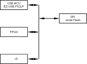 |
| TE0320 | 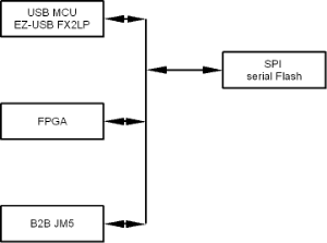 |
| TE0630 | 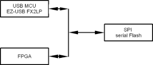 |
SPI Flash and FPGA connection; SPI Flash and USB FX2 microcontroller
FPGA SPI Configuration Interface with FX2 microcontroller and SPI Flash
FPGA SPI Configuration Interface (DATA) Pins:
- SPI/S, SPI/C , SPI_D, SPI_Q (aka CSO_B, CCLK, MOSI/DI, MISO/DO aka PD[7:4]) for TE0300 and TE0320
- CSO_B, CCLK, MOSI/DI, MISO/DO, MISO3 and MISO2 (aka PD[7:4] and MISO[3:2]) for TE0630
FPGA SPI Configuration Interface (CONTROL/STATUS) Pins: PD[3:1] for every TE USB FX2 module:
- INIT_B, DONE, FX2_PROG_B aka PROG_B (Spartan-3E and Spartan-3A) or PROGRAM_B (Spartan-6).
FX2_PS_EN (PD0) is used to control the signal PS_EN (if the switch FX2_ON is set to on), so it is not really part of the SPI Configuration Interface. The signal PS_EN could enable/disable some power rails.
FPGA SPI Configuration Interface (DATA) Pins
TE0300 (Spartan-3E) and TE0320 (Spartan-3A) module
This interface section is common to TE0300 (Spartan-3E) and TE0320 (Spartan-3A) module.
Only SPI_buswidth (for SPI Flash memory) = 1 is supported by TE0300 and TE0320 module.
Pin Name | Pin Name FPGA FPGA Direction | Pin Name FX2 FX2 direction | Description | During Configuration | After Configuration |
|---|---|---|---|---|---|
SPI/S | CSO_B of Spartan-3 Output | PD4 Output when | Master SPI Chip Select Output Active Low. Connect to the SPI Flash PROM’s Slave Select input. Chip select: When the S# input | If HSWAP or PUDC_B =1, connect this signal to a 4.7 kΩ pull-up resistor to 3.3V. | Drive CSO_B High after configuration to disable the SPI Flash and reclaim the MOSI, DIN, and CCLK pins. Optionally, re-use this pin and MOSI, DIN, and CCLK to continue communicating with SPI Flash. |
| SPI/C | CCLK Output | PD5 Output when | Configuration Clock. Generated by FPGA internal oscillator. Connect to the SPI Flash PROM’s Slave Clock input. Frequency controlled by ConfigRate bitstream generator option. If CCLK PCB trace is long or has multiple connections, terminate this output to maintain signal integrity. Clock: The C input signal provides the | Drives SPI Flash PROM’s clock input. | User I/O. Drive High or Low if not used. |
| SPI_D | MOSI Output | PD6 Output when | Master SPI Serial Data Output Connect to the SPI Flash PROM’s Slave Data Input pin. Serial data: The DQ0 input signal is | FPGA sends SPI Flash memory read commands and starting address to the PROM’s serial data input. | User I/O |
SPI_Q | DIN Input | PD7 Input, by default (2) | Master SPI Serial Data Input Connect to the SPI Flash PROM’s Slave Data Output pin. Serial data: The DQ1 output signal is | FPGA receives serial data from SPI Falsh PROM’s serial data output. | User I/O |
FPGA SPI Configuration Interface (DATA) Pins: PD[7:4] for TE0300 and TE0320 module
TE0630 (Spartan-6) module
This interface section is used only by TE0630 (Spartan-6) module.
SPI_buswidth (for SPI Flash memory) = 1 (single mode), 2 (dual mode) or 4 (quad mode) are supported by TE0630 module.
ISE procedure, for example.
- Open TE USB FX2 project
- Generate Programming File -> Process Properties
- Configuration options "-g SPI_buswidth" = 1,2 or 4 then Apply and OK
- Run "Generate programming file"
- Open iMPACT and generate msc from bit
- Program mcs to Flash in x1 (single), x2 (dual) or x4 (quad) mode
Pin Name | Pin Name FPGA | Pin Name FX2 | Description | During Configuration | After Configuration |
|---|---|---|---|---|---|
| CSO_B | CSO_B Output | PD4 Output when
| Master SPI Chip Select Output. Active Low. Connect to the SPI Flash PROM’s Slave Select input | If HSWAPEN_B =1, connect this signal to VCCO through pull-up resistor externally. | User I/O. Drive CSO_B High after configuration to disable the SPI Flash and reclaim MOSI, DIN, and CCLK pins. Optionally reuse this pin, MOSI, DIN, with SPI flashand CCLK to continue communicating |
| CCLK | CCLK Output | PD5 Output when
| Configuration clock source for all configuration modes except JTAG. Generated by FPGA internal oscillator. Connect to the SPI flash PROM’s Slave Clock input. | Drive SPI Flash’s clock input. | User I/O. Drive High or Low if not used. |
| MOSI/DI | MOSI/DI Output/Input Bidirectional | PD6 Output when
| Master FPGA Serial Data Output and Master FPGA Serial Data Input. Connect to the SPI Flash PROM’s Slave Data Input pin. It is used in x1 (single mode), | FPGA sends SPI flash memory read commands and starting address to the PROM’s serial data input. | User I/O |
MISO/DO | MISO/DO Input | PD7 Input, by default (2)
| Master FPGA Serial Data Input PROM’s Slave Data Output pin. It is used in x2 (dual mode) and x4 (quad) mode. | FPGA receives serial data from PROM’s serial data output. | User I/O |
| MISO2 and MISO3 aka MISO[3:2] | MISO3 and Input | NOT CONNECTED | Master FPGA Serial Data Input They are used in x4 (quad) mode. | Used only when using the fast-read quad output command. | User I/O |
FPGA SPI Configuration Interface (DATA) Pins: PD[7:4] and MISO[3:2] for TE0630
FPGA SPI Configuration Interface (CONTROL/STATUS) Pins
This interface section is common to all TE USB FX2 modules (TE0300,TE0320,TE0630): FPGA Spartan-3E, Spartan-3A and Spartan-6.
FX2_PS_EN is used to control the signal PS_EN (if the switch FX2_ON is set to on), so it is not really part of the SPI Configuration Interface.
Pin Name | Pin Name FPGA | Pin Name FX2 | Description | During Configuration | After Configuration |
|---|---|---|---|---|---|
| FX2_PS_EN | NOT CONNECTED | PD0 Bidirectional | Control of signal PS_EN Some power rails are controlled See Power Rails Configuration: | If the switch FX2_ON | If the switch FX2_ON is |
| FX2_PROG_B | PROGRAM_B PROG_B Input | PD1 Bidirectional Input/Output (3) | Program FPGA. Active Low. Active-Low asynchronous full-chip When asserted Low for 500 ns | Must be High to allow configuration to start. | Drive FX2_PROG_B Low Hold FX2_PROG_B to force
|
| DONE | DONE Bidirectional I/O, Open-Drain, Use a pull-up resistor (330Ω) on DONE (4). pull-up. See AR# 35002.
| PD2 Input, | Dedicated Active-High signal
Refer to the BitGen section of UG628, Command Line Tools User Guide for software settings. | See | The FX2 microcontroller's |
INIT_B | INIT_B Open-drain bidirectional I/O. Use a pull-up resistor (4.7kΩ) on INIT_B (4). See AR# 35002. | PD3 Input, | Initialization Indicator. Active Low. Goes Low at start of configuration during Initialization memory clearing process. Released at end ofmemory clearing, when mode select pins are sampled. The INIT pin does not have a rise
| Active during configuration. Before the Mode pins are sampled, INIT_B is an input that can be held Low to delay configuration. If SPI Flash PROM requires more than 2 ms to awake after powering on,hold INIT_B Low until PROM is ready. After the Mode pins are sampled, INIT_B is an open-drain active-Low output indicating whether a CRC error occurred during configuration:
| User I/O. If unused in the application, drive INIT_B High to avoid a floating value. Dual-Purpose: if User I/O if POST_CRC is not enabled. |
FPGA SPI Configuration Interface (CONTROL/STATUS) Pins: PD[3:0] for every TE USB FX2 module
Only the status of these PD2 pin (FPGA_DONE) could be retrieved using the
Legend/Explanations/References of previous tables
(1) In various function of reference firmware code spi.c.
spi.c, TE USB FX2 firmware v3.02
OED = 0x73;       // 0b01110001; => PD6,PD5,PD4,PD0 pins output enabled;
FPGA_POWER = 0;   // power off fpga
(2) For default direction of pin, see table 10 ("FX2LP Pin Descriptions") of the document "EZ-USB® FX2LP™ USB Microcontroller High-Speed USB Peripheral Controller" (link).
(3) In the reference firmware code fw.c.
fw.c, TE USB FX2 firmware v3.02
IOD = 0x03; // Enable FX2_PS_EN and FX2_PROG_B as inputs  => // 0b00000011; => PD1,PD0 pins input enabled;
OED = 0x03; // Enable FX2_PS_EN and FX2_PROG_B as outputs => // 0b00000011; => PD1,PD0 pins output enabled;
The Xilinx Official Recommendation will still stand as using a 4.7k pull-up on INIT as the device characteristics in regards to INIT have not changed from other families.The reasoning behind the recommendation for a stronger pull-up on INIT was because INIT is a User-IO after configuration.If the INIT pin is not used in the design it will be unused, and unused pins by default have a pull-down. The voltage divider created between the pull-down and the pull-up on INIT might cause the voltage to drop lower than Vihmin at Vcco for a downstream device. For this reason, using a stronger pull-up can help ensure Vihmin is met on other devices connected to the pin. The INIT pin can also be included in the user logic and driven or tri-stated accordingly.
The DONE pin is an open drain driver which is released during the Start-Up sequence at the end of configuration. Since the pin is an open drain driver, it needs a pull-up to ensure the pin goes High. The DONE pin is expected to rise within 1 clock cycle of the Start-Up sequence. The Spartan-6 Configuration User Guide (v2.1, page 24) states that "DONE should be pulled-up with a 2.4k pull-up," however, this value is a typo in the document.The official recommendation for the pull-up on a Spartan-6 deviceis the same as for theSpartan-3 family and Virtex-4, Virtex-5, and Virtex-6 devices where a 330 ohm pull-up should be used. This recommendation allows for the DONE pin to rise within 1 clock cycle at a maximum configuration rate of 100 MHz. If a board has been populated with a 2.4k pull-up on the DONE signal, the board should work fine at slower speeds (~2MHz), but you might experience Start-Up sequence issues at increased speeds. The official recommendation is to use the 330 ohm pull-up on the DONE pin, and the 2.4k might enable to device to work just fine.
In short, the DONE pin pull-up recommendation of 330 ohm and INIT pin pull-up recommendation of 4.7k that Xilinx has been using for all recent FPGA families still holds true for Spartan-6 devices and these values should be used.
Overview
Content Tools