Description
XPS_NPI_DMA is high performance direct memory access (DMA) engine which seamlessly integrates into Xilinx EDK environment (figure below). It is highly flexible due to full access of the softcore MicroBlaze to the XPS_NPI_DMA core functionality through 9 32-bit registers attached to PLBv4.6 bus.
It enables high speed data streaming to (input port) and from (output port) an external memory attached to a Xilinx Multiport Memory Controller (MPMC).
XPS_NPI_DMA and XPS_FX2 custom IP blocks are both necessary to connect (throgh USB connection) host computer's software and TE USB FX2 module's DRAM. For MB Commands tests, see example 4.
Features
- The input and output port can run simultaneously.
- The transfer on each port can have its own allocated memory space and can be looped. Loop means that when the transfer will run indefinitely on allocated memory space (like a frame buffer) until stopped.
- The data written to the input port can be stored in a memory linearly.
- The data coming out from the output port can be read in X-Y pattern. That means it can read data linearly or canjump in memory locations to transpose input data – used for rotating image for 90 degrees. That is possible when using single beat transactions (word or double-word) for reading.
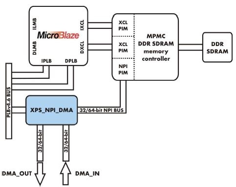
System integration block scheme
The XPS_NPI_DMA has 4 interfaces:
- Xilinx PLBv4.6 created with IPIF wizard for access to 9 x 32-bit registers. These registers control the whole peripheral operation.
- MPMC Native Port Interface (NPI) bus supporting 32 or 64-bit width. This bus is used for highspeed access to external memory.
- Proprietary synchronous 32 or 64-bit wide DMA_IN bus used for data streaming to external memory. This port can stream data in blocks – up to 64 word burst (64-bit only). Maximal sustainable bandwidth at 100MHz NPI_Clk is 200MB/s .
- Proprietary synchronous 32 or 64-bit wide DMA_OUT bus used for data streaming from external memory. The bus width is dependant on NPI bus width. This port can stream data in single beat transfers – word (32-bits), double word (64-bit), 16, 32 and 64-word (64-bit only) per one transaction. Maximal sustainable bandwidth at 100MHz NPI_Clk is approx. 300MB/s at 32-bits and 600MB/s at 64-bits.
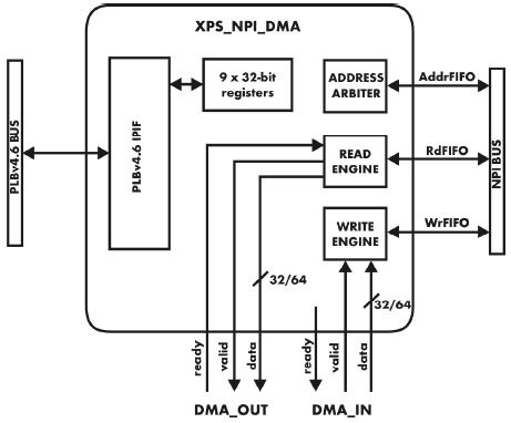
Peripheral internal structure block scheme
XPS_NPI_DMA Core Design Parameters
| Feature/Description | Parameter Name | Allowable Values | Default Value | VHDL Type |
|---|---|---|---|---|
| System Parameters | ||||
| Target FPGA family | C_FAMILY | spartan3, spartan3e, spartan3a, spartan3adsp, spartan3an, virtex2p, virtex4, qvirtex4, qrvirtex4, virtex5 | virtex5 | string |
| PLB Parameters | ||||
| PLB base address | C_BASEADDR | Valid Address | None | std_logic_vector |
| PLB high address | C_HIGHADDR | Valid Address | None | std_logic_vector |
| PLB least significant address bus width | C_SPLB_AWIDTH | 32 | 32 | integer |
| PLB data width | C_SPLB_DWIDTH | 32, 64, 128 | 32 | integer |
| Shared bus topology | C_SPLB_P2P | 0 = Shared bus topology | 0 | integer |
| PLB master ID bus Width | C_SPLB_MID_WIDTH | log2(C_SPLB_NUM_ MASTERS) with a minimum value of 1 | 1 | integer |
| Number of PLB masters | C_SPLB_NUM_MASTERS | 1 - 16 | 1 | integer |
| Width of the slave data bus | C_SPLB_NATIVE_DWIDTH | 32 | 32 | integer |
| Burst support | C_SPLB_SUPPORT_BURSTS | 0 = No burst support | 0 | integer |
| XPS_NPI_DMA Parameters | ||||
| NPI bus data width | C_NPI_DATA_WIDTH | 32, 64 | 32 | integer |
| Byte swap input data | C_SWAP_INPUT | 0, 1 | 0 | integer |
| Byte swap output data | C_SWAP_OUTPUT | 0, 1 | 0 | integer |
| Writing padding value if number of bytes does not match multiple of packet size | C_PADDING_BE | 0, 1 (zeros, ones) | 0 | integer |
XPS_NPI_DMA Core Design Parameters
XPS_NPI_DMA I/O Signal Descriptions
| Name | Interface | I/O | Initial State | Description |
|---|---|---|---|---|
| NPI_Clk | - | I | - | Memory clock |
| ChipScope[0:63] | - | O | - | Debug port |
| IP2INTC_Irpt | - | O | 0 | Interrupt request LEVEL_HIGH |
| Capture_data[(C_NPI_DATA_WIDTH-1):0] | DMA_IN | I | - | Sync DMA Input data |
| Capture_valid | DMA_IN | I | - | Sync DMA Input valid strobe |
| Capture_ready | DMA_IN | O | 0 | DMA Input is ready flag |
| Output_data[(C_NPI_DATA_WIDTH-1):0] | DMA_OUT | O | - | DMA Output data, |
| Output_valid | DMA_OUT | O | 0 | DMA Output valid strobe, sync to NPI_Clk |
| Output_ready | DMA_OUT | I | 1 | External Output ready |
| NPI_Addr[31:0] | MPMC_PIM | O | zeros | NPI address data |
| NPI_AddrReq | MPMC_PIM | O | 0 | NPI address request |
| NPI_AddrAck | MPMC_PIM | I | - | NPI address acknowledge |
| NPI_RNW | MPMC_PIM | O | 0 | NPI read now write |
| NPI_Size[3:0] | MPMC_PIM | O | 0 | NPI packet size See below for info |
| NPI_RdModWr | MPMC_PIM | O | 0 | NPI read mod write (not used) |
| NPI_WrFIFO_Data[(C_NPI_DATA_WIDTH-1):0] | MPMC_PIM | O | zeros | NPI write FIFO data vector |
| NPI_WrFIFO_BE[(C_NPI_DATA_WIDTH/8-1):0] | MPMC_PIM | O | ones | NPI write FIFO byte enable mask (alway ones) |
| NPI_WrFIFO_Push | MPMC_PIM | O | 0 | NPI write FIFO data valid strobe |
| NPI_RdFIFO_Data[(C_NPI_DATA_WIDTH-1):0] | MPMC_PIM | I | - | NPI read FIFO data vector |
| NPI_RdFIFO_Pop | MPMC_PIM | O | 0 | NPI read FIFO data read strobe |
| NPI_RdFIFO_RdWdAddr[3:0] | MPMC_PIM | I | - | NPI read FIFO read write addr (not used) |
| NPI_WrFIFO_Empty | MPMC_PIM | I | - | NPI write FIFO empty flag |
| NPI_WrFIFO_AlmostFull | MPMC_PIM | I | - | NPI write FIFO almost full flag |
| NPI_WrFIFO_Flush | MPMC_PIM | O | 0 | NPI write FIFO reset |
| NPI_RdFIFO_Empty | MPMC_PIM | I | - | NPI read FIFO empty flag |
| NPI_RdFIFO_Flush | MPMC_PIM | O | 0 | NPI read FIFO reset |
| NPI_RdFIFO_Latency[1:0] | MPMC_PIM | O | ‘’01’’ | NPI read FIFO latency |
| NPI_InitDone | MPMC_PIM | I | - | MPMC init done flag |
| OTHERS ARE PLBv4.6 SIGNALS | PLBv4.6 | - | - | - |
XPS_NPI_DMA I/O Signal Descriptions
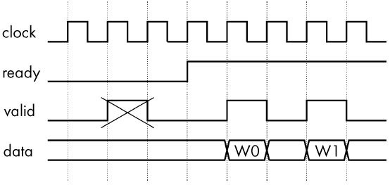
Writing and reading to/from DMA_IN and DMA_OUT ports
The point to point unidirectional buses use simple handshaking protocol.
- When (slave) “ready” signal is high the port is open for writing.
- A write is performed when “valid” signal goes high.
- The “data” should be valid when valid signal is high.
- If “valid” signal goes high and the ready is low then the data are discarded (FIFO_IN only).
- The signals are updated on rising edge of clock.
The internal clock for DMA_IN is NPI_Clk.
In this version DMA_OUT can properly throttle transmission using Ready signal only at single beat transfers (Read block size = 0).
| BUS | DMA_IN | DMA_OUT |
|---|---|---|
| Bus width | 32 or 64 bit | 32 or 64 bit |
| Clock synchronous to | NPI_Clk | NPI_Clk |
| “valid” width | Multiple cycles possible | Multiple cycles possible |
XPS_NPI_DMA I/O Signal Descriptions
DMA high speed communication ports principle of operation
XPS_NPI_DMA Core Registers
XPS_NPI_DMA has a full access of a microprocessor to the core functionality through a 9 user 32-bit and 7 IPIF Interrupt registers attached to PLBv4.6 bus.
Base Address + Offset (hex) | Register Name | Access Type | Default Value (hex) | Description |
|---|---|---|---|---|
| NPI_DMA_CORE IP Core Grouping | ||||
C_BASEADDR + 00 | CR | R/W | 0x00000000 | Control Register |
| C_BASEADDR + 04 | WSA | R/W | 0x00000000 | Write Start Address Register |
| C_BASEADDR + 08 | WBR | R/W | 0x00000000 | Write Bytes Register |
| C_BASEADDR + 0C | RSA | R/W | 0x00000000 | Read Start Address Register |
| C_BASEADDR + 10 | RBR | R/W | 0x00000000 | Read Bytes Register |
| C_BASEADDR + 14 | RJR | R/W | 0x00000000 | Read Jumps Register |
| C_BASEADDR + 18 | SR | Read | 0x00000000 | Status Register |
| C_BASEADDR + 1C | WCR | Read | WSA | Write Address Counter Register |
C_BASEADDR + 20 | RCR | Read | WBR | Read Address Counter Register |
| IPIF Interrupt Controller Core Grouping | ||||
C_BASEADDR + 200 | INTR_DISR | Read | 0x00000000 | interrupt status register |
C_BASEADDR + 204 | INTR_DIPR | Read | 0x00000000 | interrupt pending register |
C_BASEADDR + 208 | INTR_DIER | Write | 0x00000000 | interrupt enable register |
C_BASEADDR + 218 | INTR_DIIR | Write | 0x00000000 | interrupt id (priority encoder) register |
C_BASEADDR + 21C | INTR_DGIER | Write | 0x00000000 | global interrupt enable register |
C_BASEADDR + 220 | INTR_IPISR | Read | 0x00000000 | ip (user logic) interrupt status register |
| C_BASEADDR + 228 | INTR_IPIER | Write | 0x00000000 | ip (user logic) interrupt enable register |
XPS_NPI_DMA Core Registers
The First (LSB) interrupt from user_logic is masked on the left!!
Details of XPS_NPI_DMA Core Regi sters
The parts of the registers (or the whole registers) with a non-capital designation (e.g. wr_fifo_rst) are usually the names of the HDL signals connected to the described register.
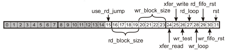
Control Register (CR)
The Control Register is used to control basic peripheral functions. All the bit flags are assembled here.
| Bits | Name | Description Reset | Value |
|---|---|---|---|
31 | rst | Peripheral soft reset (not self resettable)
| 0 |
| 30 | wr_fifo_rst
| Write FIFO reset (not self resettable) | 0 |
| 29 | rd_fifo_rst | Read FIFO reset (not self resettable) | 0 |
| 28 | wr_loop | Write loop – continuous transfer | 0 |
| 27 | rd_loop | Read loop – continuous transfer | 0 |
26 | wr_test
| Write test – writes 32bit counter to memory | 0 |
| 25 | xfer_write | Write data flag (starts/stops xfer) | 0 |
| 24 | xfer_read | Read data flag (starts/stops xfer) | 0 |
| 20-23 | wr_block_size | Write block size | 0x0 |
| 16-19 | rd_block_size | Read block size | 0x0 |
| 15 | use_rd_jump | Enables transpose | 0 |
Control Register bits
Write Start Address Register (WSA)
Here, the user inputs start address for writing transfer. It is an external memory address for the first byte to be written.
It should be aligned to Write block size boundary.

wr_start_addr
Write Bytes Register (WBR)
Here, the user inputs the number of bytes to written to memory. It is not necessary to align the number of bytes to block size, since the remaining bytes will be padded. If the user sets wr_loop to 1 then the WSA+WBR is the maximal address before the address counter jumps to WSA and starts counting again.
wr_xfer_bytes
Read Start Address Register (RSA)
Here, the user inputs start address for reading transfer. It is an external memory address for the first byte to be read.
It should be aligned to Read block size boundary.
rd_start_addr
Read Bytes Register (RBR)
Here, the user inputs the number of bytes to be read from the memory. It is not necessary to align the number of bytes to block size, since the remaining bytes will remain in the RdFIFO. If the user sets rd_loop to 1 then the when the byte counter reaches RBR values jumps to 0 (RSA address) and starts counting again.
rd_xfer_bytes
Read Jumps Register (RJR)
This register is used to input two16bit values to define the reading jumping startegy/algorithm. The read_jump is an address increment between two consecutive reads. If the user want linear read then this is a number of bytes per read block (4 or 8 for single beat xfer). When rotating (transposing) an image this should equal to number of bytes in a row. The parameter rows define how many reads should be done before returning to starting position+block size.
At linear transfer this register in NOT USED.
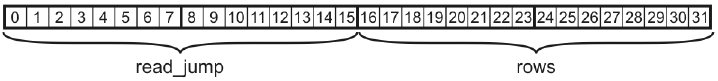
Read Jumps Register (RJR)
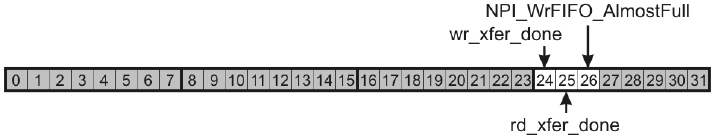
Status Register (SR)
In the status register the peripheral reports of the current status.
| Bits | Name | Description | Reset Value |
|---|---|---|---|
| 31 | wr_xfer_done | Write xfer done flag (always 0 if wr_loop = '1') | 1 |
| 30 | rd_xfer_done | Read xfer done flag (always 0 if wr_loop = 1) | 1 |
| 24-27 | xfer_status | Write xfer status (bit 27 = wr_fifo_full) | 0 |
Status Register (SR)
Write Address Counter Register (WCR)
Reading this register returns current WRITE address counter value. It can be used to monitor write transfer progress.
wr_xfer_counter
Read Address Counter Register (RCR)
Reading this register returns current READ address counter value. It can be used to monitor read transfer progress.
rd_xfer_counter
Interrupt registers
With INTR_IPIER register the user can enable/disable peripheral interrupt sources. With INTR_IPISR the user can identify interrupt source. Writing a value to INTR_IPISR also clears interrupt.
"Ghost" interrupts
The user must make sure that triggered interrupts will be cleared in a consinstent way (single owner); the user (host computer's software) must only clear triggered interrupts. Otherwise the user will trigger "ghost" interrupts which were not triggered by peripheral, but the interrupt controller itself.
Writing 0x7 to INTR_DIER will enable IP interrupt sources and writing 0x80000000 to INTR_DGIER will enable global interrupt.
The image below presents a conection of user logic interrupt to INTR_IPIER and INTR_IPISR.
Conection of user logic interrupt to INTR_IPIER and INTR_IPISR.
Programmin model
In the instruction sequence it is only important that xfer_write or xfer_read are written at the end as they start the transmission.
| Write block size | wr_block_size | C_NPI_DATA_WIDTH | type of transfer | Implemented |
|---|---|---|---|---|
| 4 bytes | X”0” | 32 | 1 word xfer | |
| 8 bytes | X”0” | 64 | 2 words xfer | |
| 16 bytes | X”1” | 32-64 | 4-word cache-line burst | |
| 32 bytes | X”2” | 32-64 | 8-word cache-line burst | |
| 64 bytes | X”3” | 32-64 | 16-word burst | |
| 128 bytes | X”4” | 32-64 | 32-word burst | |
| 256 bytes | X”5” | 64 | 64-word burst |
Write block size available
| Read block size | rd_block_size | C_NPI_DATA_WIDTH | type of transfer | Implemented |
|---|---|---|---|---|
| 4 bytes | X”0” | 32 | 1 word xfer | |
| 8 bytes | X”0” | 64 | 2 words xfer | |
| 16 bytes | X”1” | 32-64 | 4-word cache-line burst | |
| 32 bytes | X”2” | 32-64 | 8-word cache-line burst | |
| 64 bytes | X”3” | 32-64 | 16-word burst | |
| 128 bytes | X”4” | 32-64 | 32-word burst | |
| 256 bytes | X”5” | 64 | 64-word burst |
Read block size available
Example 1
Example of single write transfer from address 0x1C000000 to 0x1C00FFFF using 32-word burst
1. Write 0x1C000000 to WSA
2. Write 0x00010000 to WBR
3. Write 0x00000440 to CR
4. Poll SR until write_xfer_done = 1
Example 2
Example of single linear read transfer from address 0x1C000000 to 0x1C00FFFF using 32-word burst transaction
1. Write 0x1C000000 to RSA
2. Write 0x00010000 to RBR
3. Write 0x00004080 to CR
4. Poll SR until read_xfer_done = 1
Example 3
Example of single transpose read transfer from address 0x1C000000 at image size 750 bytes/row x 480 rows.
1. Write 0x1C000000 to RSA
2. Write 0x00057E40 to RBR
3. Write 0x02EE01DF to RJR (Note 1DF=rows-1)
4. Write 0x00010080 to CR
5. Poll SR until read_xfer_done = 1
In this case the user gets on output port 4 (at C_NPI_DATA_WIDTH = 32) or 8 (at C_NPI_DATA_WIDTH = 64) bytes per every data valid. Further demultiplexing (downto single pixel size if needed) can be done using a FIFO array (for example OUTPUT_DMA_FIFOS).
For using the software driver read function comments in:
#projec t#(or IP repository)\drivers\xps_npi_dma_v1_00_a\src\xps_npi_dma.c
Example 4 (if Reference Design is used): test XPS_NPI_DMA and XPS_FX2 using MB Commands
XPS_NPI_DMA and XPS_FX2 custom IP blocks are both necessary to connect (throgh USB connection) host computer's software and TE USB FX2 module's DRAM.
, , are used for data throughput and integrity test.
MB Commands require the XPS_I2C_SLAVE custom IP block and a proper FX2 interrupt handler (i2c_slave_int_handler() function in interrupt.c running on MicroBlaze); the FX2 interrupt handler is called to handle the signal interrupt xps_i2c_slave_0_IP2INTC_Irpt. The i2c_slave_int_handler() function actually execute the I2C delivered MB Command.
Write test should be executed before read test; otherwise the read test will fail.
Overview
Content Tools