| Page properties |
|---|
|
Template Revision 2.1 Design Name always "TE Series Name" + optional CPLD Name + "CPLD" - Change List 2.0 to 2.1
- Fix problem with pdf export and side scroll bar
- Change List 1.9.1 to 2.0
- add fix table of content
- add table size as macro
- removed page initial creator
|
Overview
Firmware for PCB CPLD with designator U26 : LCMX02-256HC
Feature Summary
- Power Management
- Reset
- CPLD JTAG
- Boot Mode
- PUDC
- ETH
- LED
- I2C
Firmware Revision and supported PCB Revision
See Document Change History
Product Specification
Port Description
| Name / opt. VHD Name | Direction | Pin | Pullup/Down | Bank Power | Description |
|---|
| LED / LED | out | 25 | NONE | 3.3VIN | Red LED D3 |
| CONFIG | out | 4 | NONE | 1.8V | ETH config pin |
| EN1 / EN1 | in | 32 | UP | 3.3VIN | B2B Power Enable - Old name from PCB REV04 and earlier : EN1 / EN_SC3 |
| JTAGEN / --- | in | 26 | --- | 3.3VIN | JTAG enable for CPLD Firmware update |
| MODE /MODE | in | 30 | UP | 3.3VIN | B2B Boot Mode Pin- Old name from PCB REV04 and earlier : MODE /MODE_SC1 |
| MODE0_R / MODE0_R | out | 12 | NONE | 3.3V | Zynq Boot Mode Pin- Old name from PCB REV04 and earlier : MODE0_R / BOOT_R0 |
| MODE2_R / MODE2_R | out | 17 | NONE | 3.3V | Zynq Boot Mode Pin- Old name from PCB REV04 and earlier : MODE2_R / BOOT_R2 |
| MODE3_R / MODE3_R | out | 13 | NONE | 3.3V | Zynq Boot Mode Pin- Old name from PCB REV04 and earlier : MODE3_R / BOOT_R3 |
| MR / MR | out | 10 | UP | 3.3V | Zynq Reset - Old name from PCB REV04 and earlier : MR / POR_B |
| SPI_SCK_FB/VCFG1 | out | 8 | NONE | 3.3V | Only for PCB REV05 and later. This pin is connected to MIO8 to change Bank 1 voltage for some applications like boundary scan to test MIOs. |
| RST / --- | --- | 9 | --- | 3.3V | / currently_not_used |
| NOSEQ / NOSEQ | inout | 29 | UP | 3.3VIN | NOSEQ pin- Old name from PCB REV04 and earlier : NOSEQ / NOSEQ_SC4 |
| PG_3V3 / PG_3V3 | in | 28 | UP | 3.3VIN | Power Good- Old name from PCB REV04 and earlier : PG_3V3 / PG_1V5 |
| PG_ALL / PG_ALL | in | 27 | UP | 3.3VIN | Power Good - Old name from PCB REV04 and earlier: PG_DDR_PWR / PG_1V8 |
| PG_MGT / PG_MGT | in | 11 | NONE | 3.3V | / currently_not_used |
| PGOOD / PGOOD | inout | 1 | UP | 3.3VIN | B2B Power Good- Old name from PCB REV04 and earlier : PGOOD / STAT_SC2 |
| PHY_LED1 | in | 5 | UP | 1.8V | PHY LED Pin |
| RESIN / RESIN | in | 23 | UP | 3.3VIN | B2B Reset - Old name from PCB REV04 and earlier : RESIN / nRST_SC0 |
| SCL33 / SCL33 | in | 14 | UP | 3.3V | I2C clock pin- Old name from PCB REV04 and earlier : SCL33 / SCL |
| SDA33 / SDA33 | inout | 16 | UP | 3.3V | I2C data pin- Old name from PCB REV04 and earlier : SDA33 / SDA |
| X0 / X0 | out | 21 | NONE | VCCIO34 | FPGA Pin K8 - Old name from PCB REV04 and earlier : X0 / XA_SC |
| X1 / X1 | out | 20 | NONE | VCCIO34 | PUDC FPGA Pin K7- Old name from PCB REV04 and earlier : X1 / XB_SC |
Functional Description
JTAG
JTAG signals routed directly through the CPLD to FPGA. Access between CPLD and FPGA can be multiplexed via JTAGENB JTAGEN pin of CPLD (pin 26) (logical one for CPLD, logical zero for FPGA). This pin is connected to B2B (JM1-pin 89) directly. On the carrier board can be this pin enabled or disabled with a dip switch.
| CPLD JTAGEN (B2B JM1-89) | Description |
|---|
| 0 | FPGA access |
| 1 | CPLD access |
Power
PGOOD is PG_3V3 and PG_ALL and EN1. There is no additional power control.
Reset
POR_B is RESIN and PG_3V3 and PG_ALL and EN1 with some delay.
PUDC
X1 can be changed by changing PUDC generic parameter in firmware source code. In released zip folder can be found all jed file according to PUDC state options.
Boot Mode
Boot mode can be set either by hardware (dip-switch) on the carrier board or by Linux console. Even after booting you can change the boot mode. After changing the boot mode FPGA is restarted automatically by CPLD. To change boot mode a state machine continuously monitors the corresponding register that can be change via I2C interface between CPLD and FPGA. After changing this register according to desired boot mode , CPLD will reset FPGA.
| Change Method | Boot Mode | CPLD PGOOD Pin (B2B Pin JM1-30) | CPLD MODE Pin (B2B Pin JM1-32) | Description |
|---|
| Hardware | JTAG | 0 | 0 |
|
| Hardware | --- | 0 | 1 |
|
| Hardware | SD Card | 1 | 0 |
|
| Hardware | QSPI | 1 | 1 |
|
| Change Method | Boot Mode | Command in Linux console | Command in FSBL | Description |
|---|
| Software | JTAG | i2cset -y 0 0x20 0x1 0x91 | iic_write8(0x20,0x1,0x91) | 0x20 is device address. 0x1 is register address. |
| Software | SD Card | i2cset -y 0 0x20 0x1 0x93 | iic_write8(0x20,0x1,0x93) 0x20 is device address. 0x1 is register address. |
|
| Software | QSPI | i2cset -y 0 0x20 0x1 0x92 | iic_write8(0x20,0x1,0x92) | 0x20 is device address. 0x1 is register address. |
|
ETH
CONFIG is constant zero. PHY_LED1 is connected to X0.
LED
| LED state | Description |
|---|
ON | Boot mode is changed by software either in linux console or by
FSBL code
.OFFBoot mode is selected only by hardware. ( Dip switch on carrier board) | FSBL code
CPLD revision,Boot mode and other features of the board will be shown by FSBL code while booting.The format of these information are shown in the following:
| CPLD Revision | Software adjusted boot mode | Existed boot modes in the programmed jed File | PUDC Mode | Current boot mode | Description |
|---|
cpld revision |
| Deactive (0) | 0 (QSPI/SD) | Pull |
down 1| 0) | JTAG (0) |
|
| Active (1) | 1 (QSPI/JTAG) | Pull-up deactivated ( |
0| 1) | QSPI (2) |
|
| ---- | 2 (JTAG/SD) | ---- | SD Card (3) |
|
| ---- | 3 (default QSPI/JTAG/SD) | ---- | ---- |
|
| Scroll Title |
|---|
| anchor | All information while booting |
|---|
| 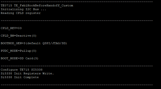 Image Removed
 |
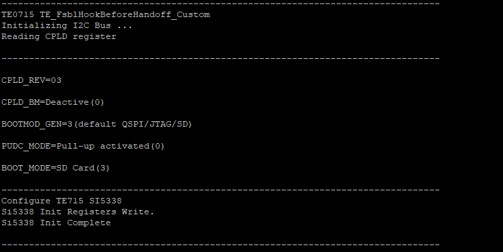 Image Added Image Added
|
MIO Bank Voltage
To implement boundary scanning (especially after the production of the board is necessary to test all MIOs), MIO Bank Voltage must be set to a certain value. From PCB revision 05 and later can be changed MIO bank voltage. According the following table the MIO bank voltage can be changed:
| Bank Voltage | Bank 1 (related pin MIO8) | Bank 0 (related pin MIO7) | Description |
|---|
| 2.5V / 3.3 V | 0 | 0 | MIO8 is pulled up in module hardware.
MIO7 is pulled down in module hardware. |
| 1.8 V | 1 | 1 |
|
For more information refer to the following site :https://support.xilinx.com/s/article/57930?language=en_US
It can be changed only state of MIO8 by firmware either in linux console or in FSBL code:
| Bank 1 Voltage | Command in linux console | Command in FSBL code | Description |
|---|
| 2.5 V / 3.3 V | i2cset -y 0 0x20 0x1 0x65 | iic_write8(0x20,0x1,0x65) | Bank 0 voltage is set in hardware in 2.5V / 3.3 V by connecting MIO7 to GND. |
| 1.8 V | i2cset -y 0 0x20 0x1 0x69 | iic_write8(0x20,0x1,0x69) |
|
After changing the MIO bank voltage FPGA will be reset and set in JTAG boot mode automatically.
To set MIO8 in floating state ( high impedance) can be executed the following commands:
| Command in linux console | Command in FSBL code |
|---|
i2cset -y 0 0x20 0x1 0x61 | iic_write8(0x20,0x1,0x61) |
LED
| LED state | Description |
|---|
| OFF | Both boot mode and MIO bank voltage in linux console or in FSBL code are not changed. |
| Slow blinking | Boot mode is changed by software either in linux console or by FSBL code. |
| Fast blinking | MIO bank 1 voltage in linux console or in FSBL code is changed. |
| ON | Both boot mode and MIO bank voltage in linux console or in FSBL code is changed. |
Appx. A: Change History and Legal Notices
Revision Changes
- Changes REV02 to REV03
- Boot mode configuration via hardware (dip switch) and firmware added (Boot mode configuration via linux console)
- Pullup or pulldown states of PORT pins was checked.
- Adding i2c to gpio ip (i2c_slave.vhd)
- Changing oscillator frequency from 12.09 MHZ to 24.18MHZ
- PORT signals according to the schematic are renamed.
- JTAG time constraint correction.
- PGOOD pin is used as boot mode selector pin.
- VCFG (MIO8) pin can be changed by i2cset command. This pin must be grounded by boundary scanning. Refer to the following site :https://support.xilinx.com/s/article/57930?language=en_US
Document Change History
To get content of older revision got to "Change History" of this page and select older document revision number.
| Page properties |
|---|
|
- Note this list must be only updated, if the document is online on public doc!
- It's semi automatically, so do following
Add new row below first Copy "Page Information Macro(date)" Macro-Preview, Metadata Version number, Author Name and description to the empty row. Important Revision number must be the same as the Wiki document revision number Update Metadata = "Page Information Macro (current-version)" Preview+1 and add Author and change description. --> this point is will be deleted on newer pdf export template - Metadata is only used of compatibility of older exports
|
| Date | Document Revision | CPLD Firmware Revision | Supported PCB Revision | Authors | Description |
|---|
| Page info |
|---|
| infoType | Modified date |
|---|
| dateFormat | yyyy-MM-dd |
|---|
| type | Flat |
|---|
|
| | Page info |
|---|
| infoType | Current version |
|---|
| prefix | v. |
|---|
| type | Flat |
|---|
|
| REV03 | REV05,REV04,REV03 | | Page info |
|---|
| infoType | Modified by |
|---|
| type | Flat |
|---|
|
| |
| v.6 | REV02 | REV04,REV03 | John Hartfiel | - REV02 , Firmware released 2015-08-18
|
| 2018-07-16 | |
|
| | Initial release |
| All |
|
| | Page info |
|---|
| modified-users |
|---|
| modified-users |
|---|
|
|
|
Legal Notices
| Include Page |
|---|
| IN:Legal Notices |
|---|
| IN:Legal Notices |
|---|
|