Page History
...
Overview
| Scroll Only (inline) |
|---|
OnlineRefer to https://shop.trenz-electronic.de/en/Download/?path=Trenz_Electronic/carrier_boards/TE0701 for downloadable version of this manual and otheradditional relatedtechnical documentsdocumentation canof be found at https://wiki.trenz-electronic.de/display/PD/TE0701 the product. |
The Trenz Electronic TE0701 Carrier Board is a base-board for 4x5 4 x 5 SoMs, which exposes the MIO- and the PS/PL-pins of the SoM module's B2B-connector-pins to accessible connectors and provides a whole range of on-board components to test and evaluate Trenz Electronic 4x5 TE 4 x 5 SoMs.
See page "4 x 5 cm carriers" to get information about the SoMs supported by the TE0701 Carrier Board.
Main Components
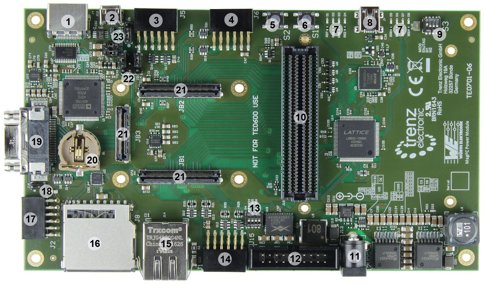
Figure 1: 4x5 4 x 5 SoM carrier board TE0701-06
...
- HDMI Connector (1.4 HEAC Support)
- Micro USB Connector (Device, Host or OTG Modes)
Pmod Connector for access to access Zynq-module's PL IO-bank pins (4 LVDS-pairs, max. VCCIO-voltage: VIOTA)
- Pmod Connector Connector for access to access for Zynq-module's PL IO-bank pins (4 LVDS-pairs, max. VCCIO-voltage: FMC_VADJ)
- User Push Button S2 ("RESTART" button by default)
- User Push Button S1 ("RESET" button by default)
- User LEDs (function mapping depends on firmware of System-Controller-CPLD)
- Mini USB Connector (USB JTAG and UART Interface)
- User 4-bit DIP Switch
- VITA 57.1 compliant FMC LPC Connector with digitally programmable FMC VADJ Power Supply
- Barrel jack for 12V Power Supply
- ARM JTAG Connector (DS-5 D-Stream) - PJTAG to EMIO multiplexing needed
- User 4-bit DIP Switch (provides the functionality to set voltage FMC_VADJ)
- Pmod Connector (J1, max. VCCIO-voltage: 3.3V): mapped to 8 Zynq PS MIO0-bank-pins (MIO0, MIO9 to MIO15), 6 pins (MIO10 to MIO15) are additionally connected to TE0701 System-Controller-CPLD
- RJ45 GbE Connector
- SD Card Connector - Zynq SDIO0 Bootable SD port
- Pmod Connector (J2, max. VCCIO-voltage: 3.3V): 6 pins (PX0 to PX5) can be multiplexed by Texas Instruments TXS02612RTWR SDIO Port Expander to MIO-pins of Zynq-module, 2 pins are connected to TE0701 System-Controller-CPLD (PX6 and PX7)
- Jumper J18
- Mini CameraLink Connector
- Battery holder for CR1220 (RTC backup voltage)
- Trenz 4x5 4 x 5 module Socket (3x Samtec LSHM Series Connectors)
- Jumper J16, J17, J21
- Jumper J9, J19, J20
...
- Overvoltage-, undervoltage- and reversed- supply-voltage-protection
- Barrel jack for 12V power supply
- Carrier Board System-Controller-CPLD Lattice MachXO2 1200HC, programable by Mini-USB JTAG-Interface J7
- Zynq-module programable by ARM-JTAG-Interface-Connector (J15) or by System-Controller-CPLD via Mini-USB JTAG-Interface J7 or JTAG-Interface on FMC-Connector J10
- Mini CameraLink
- RJ45 Gigabit Ethernet MagJack with 2 integrated LEDs.
- FPGA Mezzanine Card (FMC) Connector J10 for acces to Zynq-Module's LVDS-pairs, operable with adjustable IO-voltage FMC_VADJ
- USB JTAG- and UART-Interface (FTDI FT2232HQ) with Mini-USB-Connector J7
- ADV7511 HDMI Transmitter with HDMI-Connector J4
- 8 x user LEDs routed to System-Controller-CPLD, 8 x red
- 2 x user-push button routed to System-Controller-CPLD; by default configured as system "RESET" and "RESTART" button (depends on CPLD-Firmware)
- 2 x 4-bit DIP-Switch for base-board-configuration (3 switches routed to System-Controller-CPLD, 3 switches to set voltage FMC_VADJ, 1 switch routed to Zynq-module (MIO0), 1 switch enables Mini-USB JTAG-Interface J7)
- PMOD-Connectors to access Zynq-Module's LVDS-pairs and MIO-Pins
- Micro SD card socket, can be used to boot system
- Micro-USB-Interface (J12) connected to Zynq-module (Device, Host or OTG modes)
- Trenz 4x5 4 x 5 module Socket (3 x Samtec LSHM series connectors)
...
The TE0701 Carrier Board has on-board USB 2.0 High Speed to UART/FIFO IC FT2232HQ from FTDI. Channel A can be used as JTAG-Interface (MPSSE) to program the System-Controller-CPLD, Channel B can be used as UART-Interface routed to CPLD. There are also 4 6 additionally bus-lanes available for user-specific use. The FT2232HQ-Chip can also be used as FIFO in FT245 asynchronous mode.
There is also a standard 256 Byte EEPROM connected to the FT2232HQ-chip available to store custom configuration settings. EEPROM settings can be changed using FTDI provided tools that can be downloaded from FTDI website. See FTDI website for more informationsetting.
| Note |
|---|
Warning: By using FTDI software tools, the 256 Byte user EEPROM may be deleted without confirmation. As a consequence, the Digilent license stored in that EEPROM will also be deleted. |
USB Interface
The TE0701 Carrier Board has two physical USB-connectors:
...
| Switch | Functionality |
|---|---|
| S3-1 | CM1: Mode pin 1 (routed to Carrier Controller) |
| S3-2 | CM0: Mode pin 0 (routed to Carrier Controller) |
| S3-3 | JTAGEN: Set to ON for normal JTAG operation. Must be moved to OFF position for TE0701 System-Controller-CPLD update only |
| S3-4 | MIO0: Readable signal by System-Controller-CPLD and mounted TE07xx Module |
Table 1: Configuration of DIP-switch S3
User
...
Push-Buttons
On the TE0701 Carrier Board there are two push buttons (S1 and S2) and are routed to the System-Controller-CPLD and available to the user. The default mapping of the push buttons is as follows:
| Name | Default Mapping: | ||
|---|---|---|---|
| S1 | If S1 is pushed, the active-low RESet IN (RESIN) signal will be asserted. Note: This reset can also be forced by the FTDI USB-to-JTAG interface. | ||
| S2 | If S2 is pushed, the active-high Power ON (PON) signal (that is internally pulled-up) will be deasserted, which can be considered as a "RESTART" button to switch off (push button) and on (release button) all on-module power supplies (except 3.3VIN). Note: The capability the switch to be enabled the first time will become active shortly after Power on Reset (POR).
|
Table 2: Description of the standard functionalitys of user push-buttons S1 and S2
The functionality of the push buttons depends on the CPLD-firmware. For detailed information of the function of the push buttons, please refer to the documentation of the TE0701 System-Controller-CPLD.
...
PHY LEDs are not connected directly to the module's B2B connectors as the 4x5 4 x 5 module have no dedicated PHY LED pins assigned. PHY LED's are connected to the TE0701 System-Controller-CPLD, that can route those LED's to some module's I/O Pins. In that case the CPLD has to map the PHY LEDs to corresponding pins.
...
The on-board voltages 3.3V and 5.0V of the carrier board will be powered-up simultaneously after one single power-supply with a nominal voltage of 12V is plugged on connected to the barrel jack J10.
The on-board voltages 1.8V and 2.5V will be powered up after the module's 3.3V voltage-level has reached stable state and 3.3VOUT is available on the B2B-connector JB2, pins 9 and 11.
...
The purpose of the jumpers and the DIP-switch S4 of the Carrier Board will be explained in the following sections.
Configuring VCCIO
...
The Zynq-module's power supply is fixed to 5.0V!
...
-voltage for PL IO-bank of mounted 4 x 5 SoM
The base-board supply-voltages for the PL IO-banks of the SoM are selectable by the jumpers J16, J17 and J21. The DIP-switch S4 sets the adjustable base-board supply-voltage FMC_VADJ.
| Info |
|---|
The supply-voltage FMC_VADJ is user programmable via I2C. The setting of the adjustable voltage FMC_VADJ is done by the dedicated I2C-Bus with the lines "HDMI_SCL" and "HDMI_SDA". Therefore, a control-byte has to be send to the 8-bit control register of the I2C-to-GPIO-module of the System-Controller-CPLD. This module has the I2C-Address 0x22. To enable FMC_VADJ on TE0701, bit 7 of the control-register should be set. Note that the I2C-Bus is shared with the I2C-Interface of the HDMI-Controller. For detailed information how to set the voltage FMC_VADJ via I2C, please refer to the documentation of the TE0701 Sytem-Controller-CPLD. |
| Note |
|---|
There is also the possibility to select fixed FMC_VADJ voltages by the DIP-switch S4. Therefore, there is no need to configure any bits on |
Furthermore, the VCCIO13 supply voltage (bank 13) can be selected to be either identical to bank 33/34 (J21: 1-2, 3; jumper J16 removed) or to be FMC_VADJ (J21: 1, 2-3). Again, the latter is the default setting (i.e., VCCIO13=FMC_VADJ).
Note: The LVDS-pairs FMC_LA17 to FMC_LA33 (also PB0 to PB3 as well as Y0 to Y5) are routed to bank 13 of the Zynq-module, hence, the VCCIO13 supply voltage is chosen correspondingly by default!
...
The FMC power supply on the TE0701 Carrier Board (i.e., FMC_VADJ) is user programmable via I2C.
...
the 8-bit control register of |
...
the I2C-to-GPIO-module of the System-Controller-CPLD. |
...
To enable FMC_VADJ on TE0701, bit 7 of the control-register should be set. Note that the I2C-Bus is shared with the I2C-Interface of the HDMI-Controller.
For detailed information how to set the voltage FMC_VADJ via I2C, please refer to the documentation of the TE0701 Sytem-Controller-CPLD.
| Note |
|---|
There is also the possibility to select fixed FMC_VADJ voltages by the DIP-switch S4. Therefore, there is no need to configure any bits on the 8-bit control register of the I2C-to-GPIO-module of the System-Controller-CPLD. Note: Switch S4-4 is routed to the System-Controller-CPLD, the functionality depends on the CPLD-firmware. |
Table 3 shows the switch-configuration of the DIP-switch S4 to set the voltage FMC_VADJ.
Note: The configuration of FMC_VADJ depends on the used firmware of the System-Controller-CPLD. For detailed information, refer to the documentation of the TE0701 Sytem-Controller-CPLD.
...
S4-1
...
FMC_VADJ Value
...
Table 3: Switch S4 positions for fixed values of the FMC_VADJ voltage
Configuring 12V Power Supply Pin on the CameraLink Connector
Finally, a 12V power supply can be connected to pin 26 of the CameraLink by closing J18. However, this option is disabled by default (J18: OPEN).
Configuring Power Supply of the Micro USB Connector (Device, Host or OTG Modes)
The TE0701 carrier board can be configured as a USB host. Hence, it must provide from 5.25V to 4.75V to the board side of the downstream connection (micro USB port on J12; 13). To provide sufficient power, a TPS2051 power distribution switch is located on the carrier board in between the 5V power supply and the Vbus signal of the USB downstream port interface. If the output load exceeds the current-limit threshold, the TPS2051 limits the output current and pulls the overcurrent logic output (OC_n) low, which is routed to the on-board CPLD. The TPS2051 is put into operation by setting J19 CLOSED. J20 provides an extra 100µF decoupling capacitor (in addition to 10µF) to further stabilize the output signal. Moreover, a series terminating resistor of either 1K (J9: 1-2, 3) or 10K (J9: 1, 2-3) is selectable on the "USB-VBUS" signal. Both signals, USB-VBUS and VBUS_V_EN (that enables the TPS2051 on "high") are routed (as well as the corresponding D+/- data lines) via the on-board connector directly to the USB 2.0 high-speed transceiver PHY on the mounted SoM, which is, in turn, connected to the Zynq FPGA. In summary, the default jumper settings are the following: J9: 1-2, 3 (1K series terminating resistor); J19: CLOSED (TPS2051 in operation); J20: CLOSED (100 µF added).
Additionally, the TE0701 carrier board is equipped with a second mini USB port (J7; see (8) in Figure 1) that is connected to a "USB to multi-purpose UART/FIFO IC" from FTDI (FT2232HQ) and provides a USB-to-JTAG interface between a host PC and the TE0701 carrier board and the Zynq-module, respectively. Because it acts as a USB function device, no power switch is required (and only a ESD protection must be provided) in this case.
Summary of VCCIO-configuration via jumpers
There are two base board supply-voltages VIOTA and VIOTB connected to the 4x5 SoM's PL IO-banks. The supply-voltages have following pin assignments on B2B-connectors:
...
base-board
supply-voltages
...
base-board voltages and signals connected with
...
Table 4: base-board supply-voltages VIOTA and VIOTB
| Note |
|---|
Note: The corresponding PL IO-voltage supply voltages of the 4x5 SoM to the selectable base-board voltages VIOTA and VIOTB are depending on the mounted 4x5 SoM and varying in order of the used model. Refer to SoM's schematic to get information about the specific pin assignment on module's B2B-connectors regarding PL IO-bank supply voltages and to the 4x5 Module integration Guide for VCCIO voltage options. |
...
supported 4x5 SoMs vs
base-board VCCIO
...
B33 (VCCIOC)
B34 (VCCIOB)
...
B15 (VCCIOC)
B16 (VCCIOB)
...
B66 (HP bank, VCCIOB)
B68 (HP bank, VCCIOC)
...
B15 (VCCIOA)
B34 (VCCIOD)
...
B15 (VCCIOA)
B35 (VCCIOD)
...
B16 (VCCIOA)
B15 (VCCIOD)
...
B16 (VCCIOA)
B15 (VCCIOD)
...
B13 (VCCIOA)
B35 (VCCIOD)
...
B13 (VCCIOA)
B35 (HP bank, VCCIOD)
...
B35 (VCCIOA)
B13 (VCCIOD)
...
B13 (VCCIOA)
B12 (VCCIOD)
...
B64 (VCCIOA)
B67 (HP bank, VCCIOD)
Table 5: base-board supply-voltages VIOTA and VIOTB in conjunction with PL IO-bank voltages
...
base-board supply-voltages vs
voltage-levels
...
(J20: 1-2: additional decoupling-capacitor 100 µF)
...
Table 6: Configuration of base-board supply-voltages via jumpers. Jumper-Notification: 'Jx: 1-2, 3' means pins 1 and 2 are connected, 3 is open. 'Jx: 1, 2-3' means pins 2 and 3 are connected, 1 is open
| Note |
|---|
| It is recommended to set and measure the PL IO-bank supply-voltages before mounting of TE 4x5 module to avoid failures and damages to the functionality of the mounted SoM. |
Power On Reset (POR)
On the TE0701 the 5.0V and 3.3V power supply rails are generated by high performance DC-DC-converters from the external 12V supply. While the 3.3V plane supplies several on-board components (e.g., Lattice CPLD and FTDI Dual USB UART/FIFO IC), the 5V plane is mainly provided to power supply of the module to be carried (e.g., TE0720 Zynq SoC module). For the latter, however, special considerations must be taken (see TE0720 Power Supply). Therefore, the on-module system controller (SC) must be provided with information about the power-on-reset (POR) process, namely, the following control signals EN1, RESIN, and NOSEQ. And the SC provides, in turn, the status signal PGOOD down to the on-board System-Controller-CPLD.
...
This signal is controlled by the user push button S1 on the TE0701 and is forwarded directly to the SC, where it is latched together with the EN1 signal as well as the “all power rails OK” signal (1.0V and 1.8V for core; 1.5V and VTT for RAM, and 3.3V).
| Info |
|---|
The 3.3V power supply rail can be switched on (EN_3V3=’1’) or off (EN_3V3=’0’) by a load switch (TPS27082L) and is continuously checked by a voltage detector (TPS3805H33). Note: The 3.3VIN power supply (from which the 3.3V power plane is sourced) is supplied by the TE0701 Carrier Board and is kept always on! |
When RESIN (alias user push button S1) is not pushed and simultaneously the EN1 signal is asserted (EN='1') and all power rails are ok, the active-high Zynq power-on-reset signal PS_POR_B is asserted.
...
Note: Switch S4 is also routed to the System-Controller-CPLD, hence the VCCIO-configuration can be registered by the CPLD. Switch S4-4 is not dedicated for FMC_VADJ setting, the functionality of this switch depends on the SC-CPLD-firmware. |
Table 3 shows the switch-configuration of the DIP-switch S4 to set the voltage FMC_VADJ:
| S4-1 | S4-2 | S4-3 | FMC_VADJ Value |
|---|---|---|---|
| ON | ON | ON | 3.3V |
| OFF | ON | ON | 2.5V |
| ON | OFF | ON | 1.8V |
| OFF | OFF | ON | 1.5V |
| ON | ON | OFF | 1.25V |
Table 3: Switch S4 positions for fixed values of the FMC_VADJ voltage
Configuring 12V Power Supply Pin on the CameraLink Connector
Finally, a 12V power supply can be connected to pin 26 of the CameraLink by closing J18. However, this option is disabled by default (J18: OPEN).
Configuring Power Supply of the Micro USB Connector (Device, Host or OTG Modes)
The TE0701 carrier board can be configured as a USB host. Hence, it must provide from 5.25V to 4.75V to the board side of the downstream connection (micro USB port on J12; 13). To provide sufficient power, a TPS2051 power distribution switch is located on the carrier board in between the 5V power supply and the Vbus signal of the USB downstream port interface. If the output load exceeds the current-limit threshold, the TPS2051 limits the output current and pulls the overcurrent logic output (OC_n) low, which is routed to the on-board CPLD. The TPS2051 is put into operation by setting J19 CLOSED. J20 provides an extra 100µF decoupling capacitor (in addition to 10µF) to further stabilize the output signal. Moreover, a series terminating resistor of either 1K (J9: 1-2, 3) or 10K (J9: 1, 2-3) is selectable on the "USB-VBUS" signal. Both signals, USB-VBUS and VBUS_V_EN (that enables the TPS2051 on "high") are routed (as well as the corresponding D+/- data lines) via the on-board connector directly to the USB 2.0 high-speed transceiver PHY on the mounted SoM, which is, in turn, connected to the Zynq FPGA. In summary, the default jumper settings are the following: J9: 1-2, 3 (1K series terminating resistor); J19: CLOSED (TPS2051 in operation); J20: CLOSED (100 µF added).
Additionally, the TE0701 carrier board is equipped with a second mini USB port (J7; see (8) in Figure 1) that is connected to a "USB to multi-purpose UART/FIFO IC" from FTDI (FT2232HQ) and provides a USB-to-JTAG interface between a host PC and the TE0701 carrier board and the Zynq-module, respectively. Because it acts as a USB function device, no power switch is required (and only a ESD protection must be provided) in this case.
Summary of VCCIO-configuration via jumpers
There are two base board supply-voltages VIOTA and VIOTB connected to the 4 x 5 SoM's PL IO-banks. The supply-voltages have following pin assignments on B2B-connectors:
base-board supply-voltages | base-board B2B connector-pins | standard assignment of PL IO-bank supply-voltages on TE 4 x 5 module's B2B connectors | base-board voltages and signals connected with |
|---|---|---|---|
| VIOTA | JB2-2, JB2-4, JB2-6 | VCCIOB (JM2-1, JM2-3) / VCCIOC (JM2-5) | HDMI_SCL, HDMI_SDA, HDMI_INT, J5 VCCIO |
| VIOTB | JB1-10, JB1-12, JB2-8, JB2-10 | VCCIOA (JM1-9, JM1-11) / VCCIOD (JM2-7, JM2-9) | VCCIO1 (System-Controller-CPLD pin 55, 73) |
Table 4: base-board supply-voltages VIOTA and VIOTB
| Note |
|---|
Note: The corresponding PL IO-voltage supply voltages of the 4 x 5 SoM to the selectable base-board voltages VIOTA and VIOTB are depending on the mounted 4 x 5 SoM and varying in order of the used model. Refer to SoM's schematic to get information about the specific pin assignment on module's B2B-connectors regarding PL IO-bank supply voltages and to the 4 x 5 Module integration Guide for VCCIO voltage options. |
Following table describes how to configure the base-board supply-voltages by jumpers:
base-board supply voltages vs voltage-levels | VIOTA | VIOTB | USB-VBUS | 12V0_CL |
|---|---|---|---|---|
| 3V3 | J17:1-2, 3 & J16: open | J17: 1-2, 3 & J16: open & J21:1-2, 3 | - | - |
| 2V5 | J17:1, 2-3 & J16: open | J17:1, 2-3 & J16: open & J21: 1-2, 3 | - | - |
| FMC_VADJ | J17: open & J16: 1-2 | J21:1, 2-3 | - | - |
| 5V0 intern | - | - | J9:1-2, 3 & J19: 1-2 (J20: 1-2: additional decoupling-capacitor 100 µF) | - |
| Vbus extern | - | - | J9: 1, 2-3 & J19: open | - |
| 12V_LC | - | - | - | J18: 1-2 |
Table 5: Configuration of base-board supply-voltages via jumpers. Jumper-Notification: 'Jx: 1-2, 3' means pins 1 and 2 are connected, 3 is open. 'Jx: 1, 2-3' means pins 2 and 3 are connected, 1 is open
| Note |
|---|
| It is recommended to set and measure the PL IO-bank supply-voltages before mounting of TE 4 x 5 module to avoid failures and damages to the functionality of the mounted SoM |
Table 7: Generation of PGOOD-Signal
...
| . |
Technical Specifications
Absolute Maximum Ratings
...
| date | revision | authors | description |
|---|---|---|---|
| 2017-02-15 | Ali Naseri | added warning concerning the use of FTDI-tools | |
| 2017-0102-2515 | V40 | Ali Naseri | added power-on sequence diagram |
| 2017-01-19 | V35 | Ali Naseri | correction of table 3 (switch-positions to adjust FMC_VADJ) inserted hint to set and measure the PL IO-bank supply-voltages
|
| 2017-01-13 | V20 | Ali Naseri | added section for base-board supply- voltage configuration |
| 2016-11-29 | V10
| Ali Naseri | TRM update due to new revision 06 of the carrier board. |
| 2016-11-28 | V4 | Ali Naseri | TRM adjustment to the newest revision (05) of TE0701 Carrier Board. |
| 2014-02-18 | 0.2
| Sven-Ole Voigt | TE0701-03 (REV3) updated |
| 2014-01-05 | 0.1 | Sven-Ole Voigt | Initial release |
All |
...
Overview
Content Tools