Page History
...
| Storage Device Name | Content | Notes |
|---|---|---|
SPI Flash OTP Area | Empty, not programmed | Except serial number programmed by flash vendor. |
SPI Flash Quad Enable bit | Programmed | - |
SPI Flash main array | Demo design | - |
eFUSE USER | Not programmed | - |
eFUSE Security | Not programmed | - |
| Si5338 OTP NVM | Default settings pre-programmed | OTP not re-programmable after delivery from factory |
Signals, Interfaces and Pins
Board to Board (B2B) I/Os
Zynq MPSoC's I/O banks signals connected to the B2B connectors:
Boot Process
Trenz Electronic provides currently 2 Firmware variants, one for SD and one for QSPI usage. At the moment JTAG Mode is needed to write QSPI Flash with Xilinx Tools.
| Mode | QSPI-Variant | SD-Variant |
|---|---|---|
| Zero | JTAG | Boot from SD |
| One | Boot from Flash | JTAG |
For more information read also TE0820 CPLD - BootMode section.
Signals, Interfaces and Pins
Board to Board (B2B) I/Os
Zynq MPSoC's I/O banks signals connected to the B2B connectors:
| Bank | Type | B2B Connector | I/O | Bank | Type | B2B Connector | I/O Signal Count | Voltage | Notes |
|---|---|---|---|---|---|---|---|---|---|
64 | HP | JM2 | 48 | User | Max voltage 1.8V. | ||||
64 | HP | JM2 | 2 | User | Max voltage 1.8V. | ||||
| 65 | HP | JM2 | 18 | User | Max voltage 1.8V. | ||||
65 | HP | JM3 | 16 | User | Max voltage 1.8V. | ||||
66 | HP | JM1 | 48 | User | Max voltage 1.8V. | ||||
501 | MIO | JM1 | 6 | 1.8V | - | ||||
505 | GTR | JM3 | 4 lanes | N/A | - | ||||
505 | GTR CLK | JM3 | 1 differential input | N/A | - |
...
| Pin Name | Mode | Function | Default Configuration |
|---|---|---|---|
| EN1 | Input | Power Enable | No hard wired function on PCB, when forced low pulls POR_B low toemulate power on resetPGOOD goes low without effect on Power management. |
| PGOOD | Output | Power Good | Active high when all on-module power supplies are working properly and no PS Error occurs. |
| NOSEQ | - | - | No function. |
| RESIN | Input | Reset | Active low reset, gated to POR_B. |
| JTAGEN | Input | JTAG Select | Low for normal operation, high for CPLD JTAG access. |
Check also TE0820 CPLD.
Default PS MIO Mapping
| PS MIO | Function | B2B Pin | Connected to | PS MIO | Function | B2B Pin | Connected to | |
|---|---|---|---|---|---|---|---|---|
| 0 | SPI0 | - | U7-B2, CLK | 40..45 | - | - | Not connected | |
| 1 | SPI0 | - | U7-D2, DO/IO1 | 46 | SD | JM1-17 | B2B, SD_DAT0DAT3 | |
| 2 | SPI0 | - | U7-C4, WP/IO2 | 47 | SD | JM1-19 | B2B, SD_DAT1DAT2 | |
| 3 | SPI0 | - | U7-D4, HOLD/IO3 | 48 | SD | JM1-21 | B2B, SD_DAT2DAT1 | |
| 4 | SPI0 | - | U7-D3, DI/IO0 | 49 | SD | JM1-23 | B2B, SD_DAT3DAT0 | |
| 5 | SPI0 | - | U7-C2, CS | 50 | SD | JM1-25 | B2B, SD_CMD | |
| 6 | N/A | - | Not connected | 51 | SD | JM1-27 | B2B, SD_CLK | |
| 7 | SPI1 | - | U17-C2, CS | 52 | USB_PHY | - | U18-31, OTG-DIR | |
| 8 | SPI1 | - | U17-D3, DI/IO0 | 53 | USB_PHY | - | U18-31, OTG-DIR | |
| 9 | SPI1 | - | U17-D2, DO/IO1 | 54 | USB_PHY | - | U18-5, OTG-DATA2 | |
| 10 | SPI1 | - | U17-C4, WP/IO2 | 55 | USB_PHY | - | U18-2, OTG-NXT | |
| 11 | SPI1 | - | U17-D4, HOLD/IO3 | 56 | USB_PHY | - | U18-3, OTG-DATA0 | |
| 12 | SPI1 | - | U17-B2, CLK | 57 | USB_PHY | - | U18-4, OTG-DATA1 | |
| 13..20 | eMMC | - | U6, MMC-D0..D7 | 58 | USB_PHY | - | U18-29, OTG-STP | |
| 21 | eMMC | - | U6, MMC-CMD | 59 | USB_PHY | - | U18-6, OTG-DATA3 | |
| 22 | eMMC | - | U6, MMC-CLKR | 60 | USB_PHY | - | U18-7, OTG-DATA4 | |
| 23 | eMMC | - | U6, MMC-RST | 61 | USB_PHY | - | U18-9, OTG-DATA5 | |
| 24 | ETH | - | U8, ETH-RST | 62 | USB_PHY | - | U18-10, OTG-DATA6 | |
| 25 | USB_PHY | - | U18, OTG-RST | 63 | USB_PHY | - | U18-13, OTG-DATA7 | |
| 26 | MIO | JM1-95 | B2B | 64 | ETH | - | U8-53, ETH-TXCK | |
| 27 | MIO | JM1-93 | B2B | 65..66 | ETH | - | U8-50..51, ETH-TXD0..1 | |
| 28 | MIO | JM1-99 | B2B | 67..68 | ETH | - | U8-54..55, ETH-TXD2..3 | |
| 29 | MIO | JM1-99 | B2B | 69 | ETH | - | U8-56, ETH-TXCTL | |
| 30 | MIO | JM1-92 | B2B | 70 | ETH | - | U8-46, ETH-RXCK | |
| 31 | MIO | JM1-85 | B2B (UART RX) | 71..72 | ETH | - | U8-44..45, ETH-RXD0..1 | |
| 32 | MIO | JM1-91 | B2B (UART TX) | 73..74 | ETH | - | U8-47..48, ETH-RXD2..3 | |
| 33 | MIO | JM1-87 | B2B | 75 | ETH | - | U8-43, ETH-RXCTL | |
| 34..37 | N/A | - | Not connected | 76 | ETH | - | U8-7, ETH-MDC | |
| 38 | I2C | - | U10-12, SCL | 77 | ETH | - | U8-8, ETH-MDIO | |
| 39 | I2C | - | U10-19, SDA |
...
| PHY Pin | ZYNQ PS | ZYNQ PL | Notes |
|---|---|---|---|
| MDC/MDIO | MIO76, MIO77 | - | - |
| LED0 | - | K8 | Can be routed via PL to any free PL I/O pin in B2B connector. |
| LED1 | - | K8 | CPLD pin 17. ??? |
| LED2 | - | - | Not connected. |
| CONFIG | - | - | 1.8V |
| RESETn | MIO24 | - | - |
| RGMII | MIO64..MIO75 | - | - |
| SGMII | - | - | on B2B JM3. |
| MDI | - | - | on B2B JM3. |
...
| I2C Device | I2C Address | Notes |
|---|---|---|
Si5338A PLL | 0x70 | - |
| EEPROM | 0x53 | - |
On-board Peripherals
System Controller CPLD
Section currently not complete.
DDR4 Memory
Section currently not complete.
2 x 32 MByte Quad SPI Flash Memory
...
| Signal | Frequency | Notes |
|---|---|---|
| IN1/IN2 | - | Not used (external clock signal supply). |
IN3 | 25.000000 MHz | Fixed input clock signal from reference clock generator SiT8008BI-73-18S-25.000000E (U11). |
| IN4 | - | LSB of the default I2C address, wired to ground mean address is 0x70. |
IN5 | - | Not connected. |
IN6 | - | Wired to ground. |
| CLK0 A/B | - | Bank 65 clock input, pins K9 and J9. |
CLK1 A/B | - | MGT reference clock 3 to FPGA Bank 505 MGT. |
CLK2 A/B | - | MGT reference clock 1 to FPGA Bank 505 MGT. |
| CLK3 A/B | - | Not connected. |
Clocking
Oscillators
The module has following reference clock signals provided by on-board oscillators and external source from carrier board:
| Clock Source | Schematic Name | Frequency | Clock Destination |
|---|---|---|---|
| SiTime SiT8008BI oscillator, U21 |
| PS_CLK | 33.333333 MHz |
| ZynqMP U1,pin R16 |
CLK0_N
U10, IN3, pin 3
U8, XTAL_IN, pin 34
ETH_CLK
GTR Transceivers
The Xilinx Zynq UltraScale+ device used on the TE0820 module has 4 GTR transceivers. All 4 are wired directly to B2B connector JM3. There are also 3 clock sources for the transceivers. B505_CLK0 is connected directly to B2B connector JM3, so the clock can be provided by the carrier board. Other two clocks B505_CLK1 and B505_CLK3 are provided by the on-board clock generator (U10). As there are no capacitive coupling of the data and clock lines that are connected to the connectors, these may be required on the user’s PCB depending on the application.
On-board LEDs
There is one on-board red LED D1 wired to the PS DONE signal.
Power and Power-on Sequence
Power Supply
Power supply with minimum current capability of 3A for system startup is recommended.
Power Consumption
...
*TBD - To be determined.
Power-on Sequence
For highest efficiency of on-board DC-DC regulators, it is recommended to use same 3.3V power source for both VIN and 3.3VIN power rails. Although VIN and 3.3VIN can be powered up in any order, it is recommended to power them up simultaneously.
It is important that all carrier board I/Os are 3-stated at power-on until System Controller CPLD sets PGOOD signal high (B2B connector JM1, pin 30), or 3.3V is present on B2B connector JM2 pins 10 and 12, meaning that all on-module voltages have become stable and module is properly powered up.
See Xilinx datasheet DS925 for additional information. User should also check related carrier board documentation when choosing carrier board design for TE0715 module.
Power Rails
...
1, 3, 5
...
| SiTime SiT8008BI oscillator, U21 | - | 25.000000 MHz | Quad PLL clock generator U10, pin 3.and ETH Phy U8, pin 34 |
Table : Reference clock signals.
Gigabit Ethernet PHY
On-board Gigabit Ethernet PHY (U8) is provided with Marvell Alaska 88E1512 IC (U8). The Ethernet PHY RGMII interface is connected to the ZynqMP Ethernet3 PS GEM3. I/O voltage is fixed at 1.8V for HSTL signaling. The reference clock input of the PHY is supplied from an on-board 25.000000 MHz oscillator (U21).
High-speed USB ULPI PHY
Hi-speed USB ULPI PHY (U32) is provided with USB3320 from Microchip. The ULPI interface is connected to the Zynq PS USB0 via MIO28..39, bank 501 (see also section). The I/O voltage is fixed at 1.8V and PHY reference clock input is supplied from the on-board 52.000000 MHz oscillator (U33).
MAC Address EEPROM
A Microchip 24AA025E48 serial EEPROM (U25) contains a globally unique 48-bit node address, which is compatible with EUI-48(TM) specification. The device is organized as two blocks of 128 x 8-bit memory. One of the blocks stores the 48-bit node address and is write protected, the other block is available for application use. It is accessible over I2C bus with slave device address 0x53.
GTR Transceivers
The Xilinx Zynq UltraScale+ device used on the TE0820 module has 4 GTR transceivers. All 4 are wired directly to B2B connector JM3. There are also 3 clock sources for the transceivers. B505_CLK0 is connected directly to B2B connector JM3, so the clock can be provided by the carrier board. Other two clocks B505_CLK1 and B505_CLK3 are provided by the on-board clock generator (U10). As there are no capacitive coupling of the data and clock lines that are connected to the connectors, these may be required on the user’s PCB depending on the application.
On-board LEDs
There is one on-board red LED D1 wired to the PS DONE signal.
Power and Power-on Sequence
Power Supply
Power supply with minimum current capability of 3A for system startup is recommended.
Power Consumption
| Power Input | Typical Current |
|---|---|
| VIN | TBD* |
| 3.3VIN | TBD* |
*TBD - To be determined.
Power Distribution Dependencies
Section currently not complete.
Power-On Sequence Diagram
For highest efficiency of on-board DC-DC regulators, it is recommended to use same 3.3V power source for both VIN and 3.3VIN power rails. Although VIN and 3.3VIN can be powered up in any order, it is recommended to power them up simultaneously.
It is important that all carrier board I/Os are 3-stated at power-on until System Controller CPLD sets PGOOD signal high (B2B connector JM1, pin 30), or 3.3V is present on B2B connector JM2 pins 10 and 12, meaning that all on-module voltages have become stable and module is properly powered up.
See Xilinx datasheet DS925 for additional information. User should also check related carrier board documentation when choosing carrier board design for TE0715 module.
Section currently not complete.
Power Rails
| Power Rail Name on B2B Connector | JM1 Pins | JM2 Pins | Direction | Notes |
|---|---|---|---|---|
| VIN | 1, 3, 5 | 2, 4, 6, 8 | Input | Supply voltage from the carrier board. |
| 3.3V | - | 10, 12 | Output | Internal 3.3V voltage level. |
| 3.3VIN | 13, 15, 91 | - | Input | Supply voltage from the carrier board. |
| VCCO_64 | - | 7, 9 | Input | High performance I/O bank voltage. |
| VCCO_65 | - | 5 | Input | High performance I/O bank voltage. |
| VCCO_66 | 9, 11 | - | Input | High performance I/O bank voltage. |
Bank Voltages
| Bank | Name on Schematic | Voltage | Range |
|---|---|---|---|
| 64 HP | VCCO_64 | User | HP: 1.0V to 1.8V |
| 65 HP | VCCO_65 | User | HP: 1.0V to 1.8V |
| 66 HP | VCCO_66 | User | HP: 1.0V to 1.8V |
| 500 PSMIO | VCCO_PSIO0_500 | 1.8V | - |
| 501 PSMIO | VCCO_PSIO1_501 | 3.3V | - |
| 502 PSMIO | VCCO_PSIO2_502 | 1.8V | - |
| 503 PSCONFIG | VCCO_PSIO3_503 | 1.8V | - |
| 504 PSDDR | VCCO_PSDDR_504 | 1.2V | - |
See Xilinx Zynq UltraScale+ datasheet DS925 for the voltage ranges allowed.
Board to Board Connectors
| Include Page | ||||
|---|---|---|---|---|
|
Variants Currently In Production
Module Variant | SoC | RAM | SPI Flash | Temperature Range |
|---|---|---|---|---|
| TE0820-01-02CG-1E | XCZU2CG-1SFVC784E | 1 GByte DDR4 | 64 MByte | Extended |
| TE0820-01-03CG-1E | XCZU3CG-1SFVC784E | 1 GByte DDR4 | 64 MByte | Extended |
| TE0820-01-02EG-1E | XCZU2EG-1SFVC784E | 1 GByte DDR4 | 64 MByte | Extended |
| TE0820-01-03EG-1E | XCZU3EG-1SFVC784E | 1 GByte DDR4 | 64 MByte | Extended |
| TE0820-01-04EV-1E | XCZU4EV-1SFVC784E | 1 GByte DDR4 | 64 MByte | Extended |
| HTML |
|---|
<!--
currently not in production, but for later usage:
TE0820-01-04CG-1E XCZU4CG-1SFVC784E 1 GByte DDR4 64 MByte Extended
TE0820-01-04EV-1E XCZU4EV-1SFVC784E 1 GByte DDR4 64 MByte Extended
--> |
Technical Specifications
Absolute Maximum Ratings
Parameter | Min | Max | Units | Notes |
|---|---|---|---|---|
VIN supply voltage | -0.3 | 7.0 | V | See EN6347QI and TPS82085SIL datasheets. |
| 3.3VIN supply voltage | -0.1 | 3.75 | V | See LCMXO2-256HC and TPS27082L datasheet. |
| PS I/O supply voltage, VCCO_PSIO | -0.5 | 3.630 | V | Xilinx document DS925 |
| PS I/O input voltage | -0.5 | VCCO_PSIO + 0.55 | V | Xilinx document DS925 |
| HP I/O bank supply voltage, VCCO | -0.5 | 2.0 | V | Xilinx document DS925 |
| HP I/O bank input voltage | -0.55 | VCCO + 0.55 | V | Xilinx document DS925 |
Voltage on module JTAG pins | -0.4 | VCCO_0 + 0.55 | V | VCCO_0 is 1.8V or 3.3V nominal. Xilinx document DS925 |
Storage temperature | -40 | +85 | °C | See eMMC datasheet. |
Recommended Operating Conditions
Bank Voltages
...
See Xilinx Zynq UltraScale+ datasheet DS925 for the voltage ranges allowed.
Board to Board Connectors
...
Variants Currently In Production
...
Module Variant
...
SoC
...
Technical Specifications
...
| Parameter | Min | Max | Units | Notes |
|---|---|---|---|---|
| VIN supply voltage |
| 2. |
| 5 |
| 6. |
| 6 | V | See |
| TPS82085S datasheet |
| 3.3VIN supply voltage |
| 2. |
| 375 | 3. |
| 6 | V | See LCMXO2-256HC |
| datasheet |
| PS I/O supply voltage, VCCO_PSIO |
| 1. |
| 710 | 3. |
| 465 | V | Xilinx document DS925 |
| PS I/O input voltage |
| –0. |
| 20 | VCCO_PSIO + 0. |
| 20 | V | Xilinx document DS925 |
| HP I/O |
| banks supply voltage, VCCO |
| 1. |
| 14 |
| 3. |
| 465 | V | Xilinx document DS925 |
| HP I/O |
| banks input voltage | -0. |
| 20 | VCCO + 0. |
| 20 | V | Xilinx document DS925 |
| Voltage on module JTAG pins |
| 3. |
V
Storage temperature
-40
+85
°C
Recommended Operating Conditions
...
| 135 | 3.465 | V | For a module variant with 3.3V CONFIG bank option |
| Note |
|---|
| See Xilinx datasheet DS925 for more information about absolute maximum and recommended operating ratings for the Zynq UltraScale+ chips. |
Operating Temperature Ranges
Extended grade: 0°C to +85°C.
Module operating temperature range depends also on customer design and cooling solution. Please contact us for options.
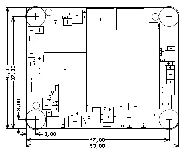
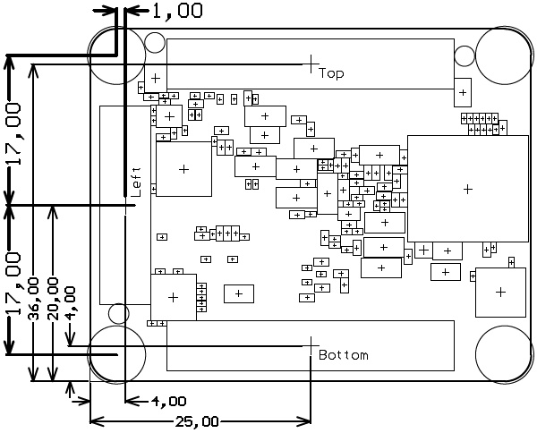
Physical Dimensions
Module size: 50 mm × 40 mm. Please download the assembly diagram for exact numbers.
Mating height with standard connectors: 8 mm
PCB thickness: 1.6 mm
Highest part on PCB: approximately 5 mm. Please download the step model for exact numbers.
All dimensions are shown in millimeters. Additional sketches, drawings and schematics can be found here.
Weight
| Variant | Weight in g | Note |
|---|---|---|
| - | - | Plain Module |
Revision History
Hardware Revision History
| Date | Revision | Notes | PCN Link | Documentation Link |
|---|---|---|---|---|
| 2017-08-17 | 02 | -- | TE0820-02 | |
| 2016-12-23 | 01 | Prototyp only | TE0820-01 |
Hardware revision number is written on the PCB board next to the module model number separated by the dash.
Document Change History
| HTML |
|---|
<!--
Generate new entry:
1.add new row below first
2.Copy "Page Information Macro(date)" Macro-Preview, Metadata Version number, Author Name and description to the empty row. Important Revision number must be the same as the Wiki document revision number
3.Update Metadata = "Page Information Macro (current-version)" Preview+1 and add Author and change description.
--> |
Date | Revision | Contributors | Description | ||||||||
|---|---|---|---|---|---|---|---|---|---|---|---|
| John Hartfiel |
| |||||||||
2017-08-07 | v.5 | Jan Kumann | Initial version. | ||||||||
all | Jan Kumann, John Hartfiel |
Table : Document change history
| Note |
|---|
| See Xilinx datasheet DS925 for more information about absolute maximum and recommended operating ratings for the Zynq UltraScale+ chips. |
Operating Temperature Ranges
Extended grade: 0°C to +85°C.
Module operating temperature range depends also on customer design and cooling solution. Please contact us for options.
Physical Dimensions
Module size: 50 mm × 40 mm. Please download the assembly diagram for exact numbers.
Mating height with standard connectors: 8 mm
PCB thickness: 1.6 mm
Highest part on PCB: approximately 5 mm. Please download the step model for exact numbers.
All dimensions are shown in millimeters. Additional sketches, drawings and schematics can be found here.
Weight
...
Boot Process
By default the TE-0820 supports SPI and SD Card boot modes which is controlled by MODE input signal from the B2B JM1 connector pin 32.
...
MODE Signal State
...
High or open
...
SPI Flash
...
Low or ground
...
SD Card
Revision History
Hardware Revision History
...
Notes
...
Hardware revision number is written on the PCB board next to the module model number separated by the dash.
Document Change History
...
Date
...
Revision
...
Authors
...
Description
...
.
Disclaimer
| Include Page | ||||
|---|---|---|---|---|
|
Overview
Content Tools