Page History
...
- Xilinx Zynq UltraScale+ MPSoC 784-pin package (ZU3EG, option for ZU5EV)
- Dual Cortex-A53 64-bit ARM v8 application processing unit (APU)
- Dual Cortex-R5 32-bit ARM v7 real-time processing unit (RPU)
Four high-speed serial I/O (HSSIO) interfaces supporting following protocols:
- PCI Express® interface version 2.1 compliant
- SATA 3.1 specification compliant interface
DisplayPort source-only interface with video resolution up to 4k x 2k
- USB 3.0 specification compliant interface implementing a 5 Gbit/s line rate
- 1 GB/s serial GMII interface
- 132 x HP PL I/Os (3 banks)
- 14 x PS MIOs (6 of the MIOs intended for SD card interface in default configuration)
- 4 x serial PS GTR transceivers
- 32-Bit DDR4, 4 GByte maximum
- Dual parallel SPI boot Flash, 512 MByte maximum
- 4 GByte eMMC (up to 64 GByte)
- GT reference clock input
- PLL for GT clocks (optional external reference)
- Gigabit Ethernet transceiver PHY (Marvell Alaska 88E1512)
- Hi-speed USB 2.0 ULPI transceiver with full OTG support (Microchip USB3320C)
- Programmable quad clock generator
- Plug-on module with 2 x 100-pin and 1 x 60-pin high-speed hermaphroditic strips
- All power supplies on board
- Size: 50 x 40 mm
Block Diagram
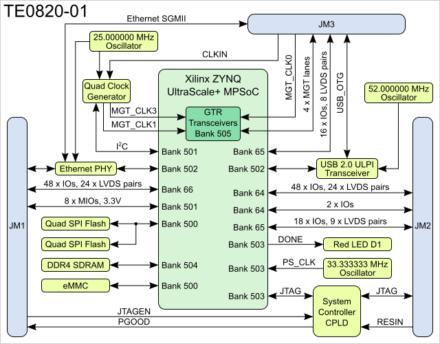
Figure 1: TE020-02 block diagram.
| Page break |
|---|
Main Components
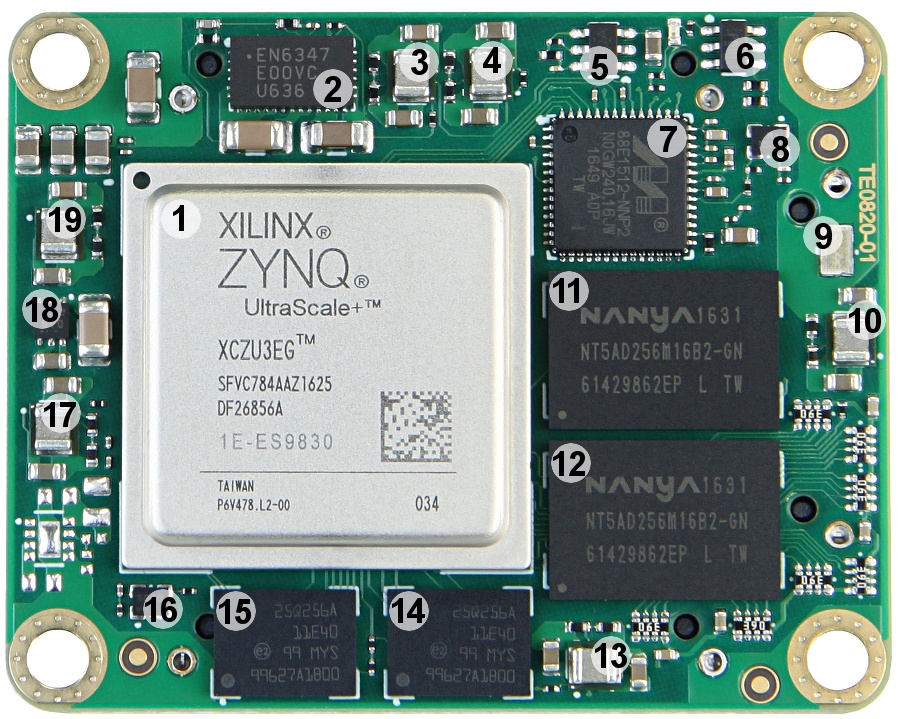
Figure 2: TE0820-02 main components.
- Xilinx Zynq UltraScale+ ZU3EG MPSoC, U1
- 4A PowerSoC DC-DC converter (PL_VCCINT, 0.85V), U5
- 3A high-efficiency step-down converter MicroSiP™ with integrated inductor (PS_AVCC, 0.9V), U9
- 3A high-efficiency step-down converter MicroSiP™ with integrated inductor (PS_AVTT, 1.8V), U13
3A PFET load switch with configurable slew rate, fast transient isolation and hysteresis control (3.3V), Q1
- Ultra-low supply-current voltage monitor with optional watchdog, U19
- Marvell Alaska 88E1512 integrated 10/100/1000 Mbps energy efficient ethernet transceiver, U8
- Low-power programmable oscillator @ 12.000000 MHz, U11
- Miniature traceability S/N pad for low-cost, unique product identification
- 3A high-efficiency step-down converter MicroSiP™ with integrated inductor (DDR_2V5, 2.5V), U4
- 4 Gbit (256 x 16) DDR4 SDRAM, U3
- 4 Gbit (256 x 16) DDR4 SDRAM, U2
- 3A high-efficiency step-down converter MicroSiP™ with integrated inductor (DDR_1V2, 1.2V), U15
- 1.8V, 256 Mbit multiple I/O serial flash memory, U17
- 1.8V, 256 Mbit multiple I/O serial flash memory, U7
- Low-power programmable oscillator @ 33.333333 MHz, U32
- 3A high-efficiency step-down converter MicroSiP™ with integrated inductor (PS_VCCINT, 0.85V), U12
- 350 mA, ultra-low VIN, RF low-dropout linear regulator with bias pin (PS_PLL, 1.2V), U23
- 3A high-efficiency step-down converter MicroSiP™ with integrated inductor (1.8V), U20
- B2B connector Samtec Razor Beam™ LSHM-150, JM2
- DDR termination regulator with VTTREF buffered reference, U16
- Low-power programmable oscillator @ 52.000000 MHz, U14
- Highly integrated full featured hi-speed USB 2.0 ULPI transceiver, U18
- B2B connector Samtec Razor Beam™ LSHM-130, JM3
- I2C programmable, any frequency , any output quad clock generator, U10
- B2B connector Samtec Razor Beam™ LSHM-150, JM1
- Lattice Semiconductor MachXO2 System Controller CPLD, U21
- 4 GByte eMMC memory, U6
...
| Storage Device Name | Content | Notes |
|---|---|---|
SPI Flash OTP Area | Empty, not programmed | Except serial number programmed by flash vendor. |
SPI Flash Quad Enable bit | Programmed | - |
SPI Flash main array | Demo design | - |
eFUSE USER | Not programmed | - |
eFUSE Security | Not programmed | - |
| Si5338 OTP NVM | Default settings pre-programmed | OTP not re-programmable after delivery from factory |
Table 1: Initial delivery state of programmable devices on the module.
Boot Process
Two different firmware versions are available, one with the QSPI boot option and other with the SD Card boot option.
| B2B JM1 MODE Pin | QSPI Firmware Version | SD Card Firmware Version |
|---|---|---|
| Low | JTAG | Boot from SD Card |
| High | Boot from Flash | JTAG |
Table 2: Boot mode pin description.
For more information refer to the TE0820 CPLD - BootMode section.
...
| Bank | Type | B2B Connector | I/O Signal Count | Voltage | Notes |
|---|---|---|---|---|---|
64 | HP | JM2 | 48 | User | Max voltage 1.8V. |
64 | HP | JM2 | 2 | User | Max voltage 1.8V. |
| 65 | HP | JM2 | 18 | User | Max voltage 1.8V. |
65 | HP | JM3 | 16 | User | Max voltage 1.8V. |
66 | HP | JM1 | 48 | User | Max voltage 1.8V. |
501 | MIO | JM1 | 6 | 1.8V | - |
505 | GTR | JM3 | 4 lanes | N/A | - |
505 | GTR CLK | JM3 | 1 differential input | N/A | - |
Table 3: General overview of board to board I/O signals.
For detailed information about the pin-out, please refer to the Pin-out table.
...
JTAG Signal | B2B Connector Pin |
|---|---|
| TMS | JM2-93 |
| TDI | JM2-95 |
| TDO | JM2-97 |
| TCK | JM2-99 |
Table 4: JTAG interface signals.
Pin 89 JTAGEN of B2B connector JM1 is used to control which device is accessible via JTAG. If set to low or grounded, JTAG interface will be routed to the Xilinx Zynq MPSoC. If pulled high, JTAG interface will be routed to the System Controller CPLD.
...
| Pin Name | Mode | Function | Default Configuration |
|---|---|---|---|
| EN1 | Input | Power Enable | No hard wired function on PCB, when . When forced low, pulls up PGOOD, goes low without effect on Power power management. |
| PGOOD | Output | Power Good | Active high when all on-module power supplies are working properly and no PS Error occurs.. |
| NOSEQ | - | - | No function. |
| RESIN | Input | Reset | Active low reset, gated to POR_B. |
| JTAGEN | Input | JTAG Select | Low for normal operation, high for CPLD JTAG access. |
Table 5: System Controller CPLD special purpose pins.
Check also TE0820 CPLD.
Default PS MIO Mapping
| PS MIO | Function | B2B Pin | Connected to | PS MIO | Function | B2B Pin | Connected to | |
|---|---|---|---|---|---|---|---|---|
| 0 | SPI0 | - | U7-B2, CLK | 40..45 | - | - | Not connected | |
| 1 | SPI0 | - | U7-D2, DO/IO1 | 46 | SD | JM1-17 | B2B, SD_DAT3 | |
| 2 | SPI0 | - | U7-C4, WP/IO2 | 47 | SD | JM1-19 | B2B, SD_DAT2 | |
| 3 | SPI0 | - | U7-D4, HOLD/IO3 | 48 | SD | JM1-21 | B2B, SD_DAT1 | |
| 4 | SPI0 | - | U7-D3, DI/IO0 | 49 | SD | JM1-23 | B2B, SD_DAT0 | |
| 5 | SPI0 | - | U7-C2, CS | 50 | SD | JM1-25 | B2B, SD_CMD | |
| 6 | N/A | - | Not connected | 51 | SD | JM1-27 | B2B, SD_CLK | |
| 7 | SPI1 | - | U17-C2, CS | 52 | USB_PHY | - | U18-31, OTG-DIR | |
| 8 | SPI1 | - | U17-D3, DI/IO0 | 53 | USB_PHY | - | U18-31, OTG-DIR | |
| 9 | SPI1 | - | U17-D2, DO/IO1 | 54 | USB_PHY | - | U18-5, OTG-DATA2 | |
| 10 | SPI1 | - | U17-C4, WP/IO2 | 55 | USB_PHY | - | U18-2, OTG-NXT | |
| 11 | SPI1 | - | U17-D4, HOLD/IO3 | 56 | USB_PHY | - | U18-3, OTG-DATA0 | |
| 12 | SPI1 | - | U17-B2, CLK | 57 | USB_PHY | - | U18-4, OTG-DATA1 | |
| 13..20 | eMMC | - | U6, MMC-D0..D7 | 58 | USB_PHY | - | U18-29, OTG-STP | |
| 21 | eMMC | - | U6, MMC-CMD | 59 | USB_PHY | - | U18-6, OTG-DATA3 | |
| 22 | eMMC | - | U6, MMC-CLKR | 60 | USB_PHY | - | U18-7, OTG-DATA4 | |
| 23 | eMMC | - | U6, MMC-RST | 61 | USB_PHY | - | U18-9, OTG-DATA5 | |
| 24 | ETH | - | U8, ETH-RST | 62 | USB_PHY | - | U18-10, OTG-DATA6 | |
| 25 | USB_PHY | - | U18, OTG-RST | 63 | USB_PHY | - | U18-13, OTG-DATA7 | |
| 26 | MIO | JM1-95 | B2B | 64 | ETH | - | U8-53, ETH-TXCK | |
| 27 | MIO | JM1-93 | B2B | 65..66 | ETH | - | U8-50..51, ETH-TXD0..1 | |
| 28 | MIO | JM1-99 | B2B | 67..68 | ETH | - | U8-54..55, ETH-TXD2..3 | |
| 29 | MIO | JM1-99 | B2B | 69 | ETH | - | U8-56, ETH-TXCTL | |
| 30 | MIO | JM1-92 | B2B | 70 | ETH | - | U8-46, ETH-RXCK | |
| 31 | MIO | JM1-85 | B2B (UART RX) | 71..72 | ETH | - | U8-44..45, ETH-RXD0..1 | |
| 32 | MIO | JM1-91 | B2B (UART TX) | 73..74 | ETH | - | U8-47..48, ETH-RXD2..3 | |
| 33 | MIO | JM1-87 | B2B | 75 | ETH | - | U8-43, ETH-RXCTL | |
| 34..37 | N/A | - | Not connected | 76 | ETH | - | U8-7, ETH-MDC | |
| 38 | I2C | - | U10-12, SCL | 77 | ETH | - | U8-8, ETH-MDIO | |
| 39 | I2C | - | U10-19, SDA |
Table 6: TE0820-02 PS MIO mapping.
Gigabit Ethernet
On-board Gigabit Ethernet PHY is provided with Marvell Alaska 88E1512 chip. The Ethernet PHY RGMII interface is connected to the Zynq Ethernet0 PS GEM0. I/O voltage is fixed at 1.8V for HSTL signaling. SGMII (SFP copper or fiber) can be used directly with the Ethernet PHY, as the SGMII pins are available on the B2B connector JM3. The reference clock input of the PHY is supplied from an on-board 25MHz oscillator (U11), the 125MHz output clock is left unconnected.
...
| PHY Pin | ZYNQ PS | ZYNQ PL | Notes | |||
|---|---|---|---|---|---|---|
| MDC/MDIO | MIO76, MIO77 | - | - | |||
| LED0 | - | K8 | Can be routed via PL to any free PL I/O pin in B2B connector. | |||
| LED1 | - | K8- | CPLD pin 17. | |||
| LED2 | - | - | Not connected. | |||
| CONFIG | - | - | Wired to the 1.8V. | |||
| RESETn | MIO24 | - | - | |||
| RGMII | MIO64..MIO75 | - | - | |||
| SGMII | - | - | on Routed to the B2B connector JM3. | MDI | - | - | on B2B JM3
Table 7: General overview of the Gigabit Ethernet PHY signals.
| Page break |
|---|
USB Interface
USB PHY is provided by Microchip USB3320. The ULPI interface is connected to the Zynq PS USB0. I/O voltage is fixed at 1.8V. Reference clock input for the USB PHY is supplied by the on-board 25.000000 MHz oscillator (U15).
...
| PHY Pin | ZYNQ Pin | B2B Name | Notes |
|---|---|---|---|
| ULPI | MIO52..63 | - | Zynq USB0 MIO pins are connected to the USB PHY. |
| REFCLK | - | - | 52.000000 MHz from on-board oscillator (U14). |
| REFSEL[0..2] | - | - | Reference clock frequency select, all set to GND selects 52.000000 MHz. |
| RESETB | MIO25 | - | Active low reset. |
| CLKOUT | MIO52 | - | Connected to 1.8V, selects reference clock operation mode. |
| DP, DM | - | OTG_D_P, OTG_D_N | USB data lines routed to B2B connector JM3 pins 47 and 49. |
| CPEN | - | VBUS_V_EN | External USB power switch active high enable signal, routed to JM3 pin 17. |
| VBUS | - | USB_VBUS | Connect to USB VBUS via a series of resistors, see reference schematics, routed to JM3 pin 55. |
| ID | - | OTG_ID | For an A-device connect to ground, for a B-device left floating. routed from JM3 pin 23. |
Table 8: General overview of the USB PHY signals.
I2C Interface
On-board I2C devices are connected to MIO38 (SCL) and MIO39 (SDA) which are configured as I2C1 by default. I2C addresses for on-board devices are listed in the table below:
| I2C Device | I2C Address | Notes |
|---|---|---|
Si5338A PLL | 0x70 | - |
| EEPROM | 0x53 | - |
Table 9: Address table of the I2C bus slave devices.
On-On-board Peripherals
System Controller CPLD
...
| Signal | Frequency | Notes |
|---|---|---|
| IN1/IN2 | - | Not used (external clock signal supply). |
IN3 | 25.000000 MHz | Fixed input clock signal from reference clock generator SiT8008BI-73-18S-25.000000E (U11). |
| IN4 | - | LSB of the default I2C address, wired to ground mean address is 0x70. |
IN5 | - | Not connected. |
IN6 | - | Wired to ground. |
| CLK0 A/B | - | Bank 65 clock input, pins K9 and J9. |
CLK1 A/B | - | MGT reference clock 3 to FPGA Bank 505 MGT. |
CLK2 A/B | - | MGT reference clock 1 to FPGA Bank 505 MGT. |
| CLK3 A/B | - | Not connected. |
Table 10: General overview of the on-board quad clock generator I/O signals.
Oscillators
The module has following reference clock signals provided by on-board oscillators and external source from carrier board:
| Clock Source | Schematic Name | Frequency | Clock Destination |
|---|---|---|---|
| SiTime SiT8008BI oscillator, U21 | PS_CLK | 33.333333 MHz | ZynqMP Zynq MPSoC U1,pin R16 |
| SiTime SiT8008BI oscillator, U21 | - | 25.000000 MHz | Quad PLL clock generator U10, pin 3., and ETH Phy Ethernet PHY U8, pin 34 |
Table 11: Reference clock signals.
...
| Power Input | Typical Current |
|---|---|
| VIN | TBD* |
| 3.3VIN | TBD* |
Table 12: Power consumption.
*TBD - To be determined.
Power Distribution Dependencies
Section currently not complete.
Power-On Sequence Diagram
Module has two power input rails which can be connected to the single power source.
Figure 3: TE0820-02 power distribution diagram.
Power-On Sequence Diagram
For highest efficiency of on-board DC-DC regulators, it is recommended to use same 3.3V power source for both VIN and 3.3VIN power rails. Although VIN and 3.3VIN can be powered up in any order, it is recommended to power them up simultaneously.
...
| Power Rail Name on B2B Connector | JM1 Pins | JM2 Pins | Direction | Notes |
|---|---|---|---|---|
| VIN | 1, 3, 5 | 2, 4, 6, 8 | Input | Supply voltage from the carrier board. |
| 3.3V | - | 10, 12 | Output | Internal 3.3V voltage level. |
| 3.3VIN | 13, 15, 91 | - | Input | Supply voltage from the carrier board. |
| VCCO_64 | - | 7, 9 | Input | High performance I/O bank voltage. |
| VCCO_65 | - | 5 | Input | High performance I/O bank voltage. |
| VCCO_66 | 9, 11 | - | Input | High performance I/O bank voltage. |
Table 13: Te0820-02 power rails.
Bank Voltages
| Bank | Name on Schematic | Voltage | Range |
|---|---|---|---|
| 64 HP | VCCO_64 | User | HP: 1.0V to 1.8V |
| 65 HP | VCCO_65 | User | HP: 1.0V to 1.8V |
| 66 HP | VCCO_66 | User | HP: 1.0V to 1.8V |
| 500 PSMIO | VCCO_PSIO0_500 | 1.8V | - |
| 501 PSMIO | VCCO_PSIO1_501 | 3.3V | - |
| 502 PSMIO | VCCO_PSIO2_502 | 1.8V | - |
| 503 PSCONFIG | VCCO_PSIO3_503 | 1.8V | - |
| 504 PSDDR | VCCO_PSDDR_504 | 1.2V | - |
Table 14: TE0820-02 I/O bank voltages.
See Xilinx Zynq UltraScale+ datasheet DS925 for the voltage ranges allowed.
...
Module Variant | SoC | RAM | SPI Flash | Temperature Range |
|---|---|---|---|---|
| TE0820-02-02CG-1E | XCZU2CG-1SFVC784E | 1 GByte DDR4 | 64 MByte | Extended |
| TE0820-02-03CG-1E | XCZU3CG-1SFVC784E | 1 GByte DDR4 | 64 MByte | Extended |
| TE0820-02-02EG-1E | XCZU2EG-1SFVC784E | 1 GByte DDR4 | 64 MByte | Extended |
| TE0820-02-03EG-1E | XCZU3EG-1SFVC784E | 1 GByte DDR4 | 64 MByte | Extended |
Table 15: TE0820-02 variants.
| HTML |
|---|
<!-- currently not in production, but for later usage: TE0820-02-04CG-1E XCZU4CG-1SFVC784E 1 GByte DDR4 64 MByte Extended TE0820-02-04EV-1E XCZU4EV-1SFVC784E 1 GByte DDR4 64 MByte Extended --> |
...
Parameter | Min | Max | Units | Notes |
|---|---|---|---|---|
VIN supply voltage | -0.3 | 7.0 | V | See EN6347QI and TPS82085SIL datasheets. |
| 3.3VIN supply voltage | -0.1 | 3.75 | V | See LCMXO2-256HC and TPS27082L datasheet. |
| PS I/O supply voltage, VCCO_PSIO | -0.5 | 3.630 | V | Xilinx document DS925 |
| PS I/O input voltage | -0.5 | VCCO_PSIO + 0.55 | V | Xilinx document DS925 |
| HP I/O bank supply voltage, VCCO | -0.5 | 2.0 | V | Xilinx document DS925 |
| HP I/O bank input voltage | -0.55 | VCCO + 0.55 | V | Xilinx document DS925 |
Voltage on module JTAG pins | -0.4 | VCCO_0 + 0.55 | V | VCCO_0 is 1.8V or 3.3V nominal. Xilinx document DS925 |
Storage temperature | -40 | +85 | °C | See eMMC datasheet. |
Table 16: Module absolute maximum ratings.
Recommended Operating Conditions
| Parameter | Min | Max | Units | Notes |
|---|---|---|---|---|
| VIN supply voltage | 2.5 | 6.6 | V | See TPS82085S datasheet |
| 3.3VIN supply voltage | 2.375 | 3.6 | V | See LCMXO2-256HC datasheet |
| PS I/O supply voltage, VCCO_PSIO | 1.710 | 3.465 | V | Xilinx document DS925 |
| PS I/O input voltage | –0.20 | VCCO_PSIO + 0.20 | V | Xilinx document DS925 |
| HP I/O banks supply voltage, VCCO | 1.14 | 3.465 | V | Xilinx document DS925 |
| HP I/O banks input voltage | -0.20 | VCCO + 0.20 | V | Xilinx document DS925 |
| Voltage on module JTAG pins | 3.135 | 3.465 | V | For a module variant with 3.3V CONFIG bank option |
Table 17: Recommended operating conditions.
| Note |
|---|
| See Xilinx datasheet DS925 for more information about absolute maximum and recommended operating ratings for the Zynq UltraScale+ chips. |
...
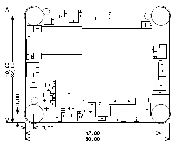
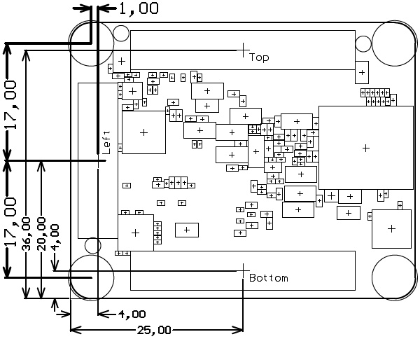
All dimensions are shown in millimeters. Additional sketches, drawings and schematics can be found here.
Weight
...
Figure 4: TE0820 module physical dimensions.
Revision History
Hardware Revision History
| Date | Revision | Notes | PCN Link | Documentation Link |
|---|---|---|---|---|
| 2017-08-17 | 02 | -- | TE0820-02 | |
| 2016-12-23 | 01 | Prototype only | TE0820-01 |
Table 18: Hardware revision history table.
Hardware revision number is written on the PCB board next to the module model number separated by the dash.
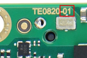
Figure 5: TE0820 module hardware revision.
Document Change History
...
Date | Revision | Contributors | Description | ||||||||
|---|---|---|---|---|---|---|---|---|---|---|---|
| Jan Kumann | Power distribution diagram added. TRM update to the template revision 1.6 Weight section removed. Few minor corrections. | |||||||||
2017-08-18 | V.7 | John Hartfiel |
| ||||||||
2017-08-07 | vV.5 | Jan Kumann | Initial version. | ||||||||
allAll | Jan Kumann, John Hartfiel |
Table 19: Document change history.
...
Overview
Content Tools