Page History
...
Board to Board (B2B) I/Os
Overview of the I/O signals signal banks connected to the FPGAs I/O banks and B2B connectorB2B connectors:
| Bank | Type | B2B Connector | I/O Signal Count | Voltage | Notes |
|---|---|---|---|---|---|
0 | HR | - | - | 3.3V | Configuration bank. |
12 | HR | JM2 | 50 I/Os, 24 LVDS pairs | User |
Supported voltage level from 1.2V to 3.3V |
. NOTE: BANK 12 IS NOT AVAILABLE ON THE K70T DEVICE |
! | ||||
13 | HR | JM1 | 48 I/Os, 24 LVDS pairs | User |
| Supported voltage level from 1.2V to 3.3V |
| . | |||||
14 | HR | JM1 JM3 | 8 I/Os 4 I/Os, 2 LVDS pairs | 3.3V | IO pins at B2B connector JM1, support only 3.3V |
| . | ||||
15 | HR | JM2 | 18 I/Os, 9 LVDS pairs | User |
| Supported voltage level from 1.2V to 3.3V |
| . | ||||
16 | HR | JM3 | 16 I/Os, 8 LVDS pairs | User |
| Supported voltage level from 1.2V to 3.3V |
| . | |||||
32 | HP | NC | - | - | Bank not used. |
33 | HP | NC | - | - | Bank not used. |
| 34 | HP | NC | - | - | Bank not used. |
Table 2: Voltage ranges and pin-outs of available logic banks of the FPGAAvailable I/O signal banks connected to the B2B connectors.
Please use Master Pin-out Table table as primary reference for the pin mapping information.
...
Figure 5: System Controller CPLD block diagram.
Power and Power-On Sequence
...
For highest efficiency of on board DC/-DC regulators, it is recommended to use same 3.3V power source for both VIN and 3.3VIN power rails. Although VIN and 3.3VIN can be powered up in any order, it is recommended to power them up simultaneously.
It is important that all baseboard I/O's Os are 3-stated at power-on until System Controller sets PGOOD signal high (B2B connector JM1, pin 30), or 3.3V is present on B2B connector JM2 pins 10,12 or 91, meaning that all on-module voltages have become stable and module is properly powered up.
See Xilinx datasheet DS182 ( for Kintex7) for additional information. User should also check related baseboard documentation when choosing baseboard design for TE0741 module.
The FPGA 1.0V supply is derived from two regulators operating in a parallel allowing higher load currents. To start the power-on sequence, pin EN1 (JM1-28, enable 1.0V voltage regulators) is by default high. By driving EN1 pin low on base-board the power-on sequence will not start until the EN1 pin is released to high.
A 3.3V supply is also needed and must be supplied from the user's PCB. An output 3.3V supply is available on some of the board connector pins (see section 'Power Rails'). The input 3.3VIN will be switched to the internal 3.3V voltage level after the FPGA 1.0V supply is stable. Than this power supply will be available on the B2B connector pins.
The regulators can be powered from the 3.3V supply or a 5V supply if preferred. The options for powering the board are detailed below.
- Apply 5V to pins VIN and 3.3V to pins 3.3VIN on the board connector
- Apply 3.3V to pins VIN and 3.3VIN on the board connectors.
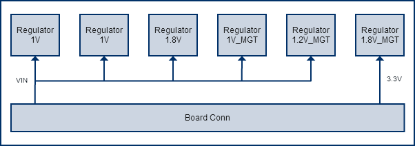
Figure 6: Connections between the on-board DC-DC and LDO regulators-28, enable 1.0V voltage regulators) is by default high. By driving EN1 pin low on base-board the power-on sequence will not start until the EN1 pin is released to high.
| Page break |
|---|
Power Rails
Voltages on B2B-Connectors | B2B JM1 Pin | B2B JM2 Pin | B2B Direction | Note |
|---|---|---|---|---|
| VIN | 1, 3, 5 | 2, 4, 6, 8 | Input | Supply voltage. |
| 3.3VIN | 13, 15 | - | Input | Supply voltage. |
| VCCIO12 | - | 7, 9 | Input | High range bank voltage. |
| VCCIO13 | 9, 11 | - | Input | High range bank voltage. |
| VCCIO15 | - | 5 | Input | High range bank voltage. |
| VCCIO16 | - | 1, 3 | Input | High range bank voltage. |
| 3.3V | - | 10, 12, 91 | Output | Internal 3.3V voltage level. |
...
- Module size: 50 mm × 40 mm
- Mating height with standard connectors: 8mm
- PCB thickness: 1.6mm
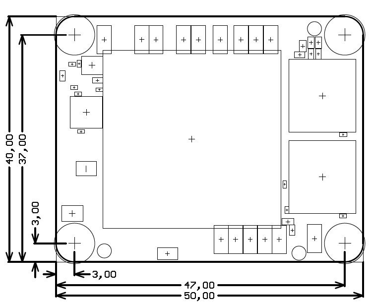
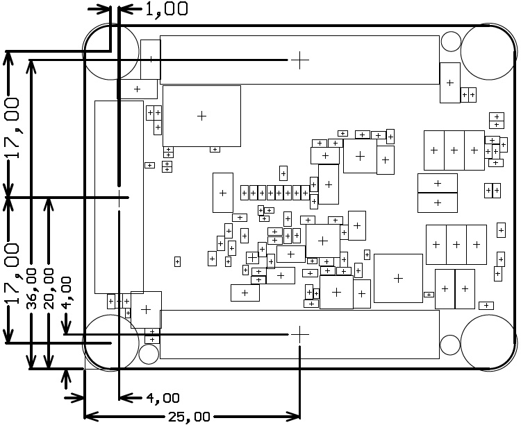
Figure 76: Physical dimensions of the TE0741 module. All dimensions are shown in millimeters.
...
Hardware revision number is written on the PCB board together with the module model number separated by the dash.


Figure 7: TE0741 PCB revision number.
Document Change History
| Date | Revision | Contributors | Description | ||||||||
|---|---|---|---|---|---|---|---|---|---|---|---|
| Jan Kumann | New power-on diagram. Few improvements. Template revision added. | |||||||||
| 2017-07-20 | v.57 | John Hartfiel | Correction: PLL default output CLKs. | ||||||||
| 2017-06-07 | v.55 | Jan Kumann | Minor formatting | ||||||||
| 2017-06-02 | v.50 | Jan Kumann | REV03 specific update. | ||||||||
| 2017-01-22 | v.42 | Jan Kumann | New block diagram added. | ||||||||
| 2017-01-13 | v.38 | Jan Kumann | New product images and physical dimension drawings. Formatting improvements and small corrections. | ||||||||
| 2017-01-12 | v.21 | John Hartfiel | Correction: B2B and FPGA bank location. | ||||||||
| 2016-12-14 | v.19 | Ali Naseri | TRM revision. | ||||||||
| 2013-12-02 | v.1 | Antti Lukats, Jon Bean | Initial version. |
...
Overview
Content Tools