Table of Contents
Overview
Trenz Electronic TE0741 is an industrial-grade FPGA module integrating a Xilinx Kintex-7 FPGA, 32 MByte SPI Flash memory for configuration and operation, and powerful switching-mode power supplies for all on-board voltages. A large number of configurable I/Os is provided via rugged high-speed stacking strips.
The TE0741 module is available in four different logic densities (70T, 160T, 325T and 410T). The 70T and 160T devices can be programmed with the free Xilinx Vivado WebPACK software. Further information about the Kintex-7 FPGA can be found in the Xilinx document 7 Series FPGA's Overview (DS180).
Key Features
- Industrial-grade Xilinx Kintex-7 FPGA module (70T*, 160T*, 325T, 410T)
* Devices supported by the free Xilinx Vivado WebPACK software. - 256-Mbit (32-MByte) Quad SPI Flash memory (for configuration and operation) accessible through:
- FPGA
- JTAG port (SPI indirect (Bus width x4))
- 8 GTX transceivers
- FPGA configuration through:
- JTAG (B2B connector)
- SPI Flash memory
- 25 MHz low jitter oscillator with shutdown control
- Programmable quad PLL clock generator
- On-board high-efficiency DC-DC converters
- GTX voltage regulators with control enable
- Core voltage regulator: 20A (2 x Enpirion DC-DC regulators with load-sharing)
- Supply voltages: either 3.3V or 3.3V and 5V
- Plug-on module with two 100-pin and one 60-pin high-speed hermaphroditic stacking strips
- Up to 144 (94 for 70T) FPGA I/O pins are available on B2B strips (up to 65 LVDS pairs possible)
- 2 user LED's, 1x DONE FPGA pin LED, 1 System Controller status LED
- System management and power sequencing
- AES bit-stream encryption
- eFUSE bit-stream encryption
- Evenly spread supply pins for good signal integrity
Additional assembly options are available for cost or performance optimization upon request.
Block Diagram
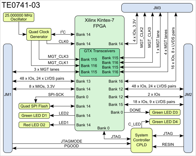
Figure 1: TE0741 block diagram.
Main Components
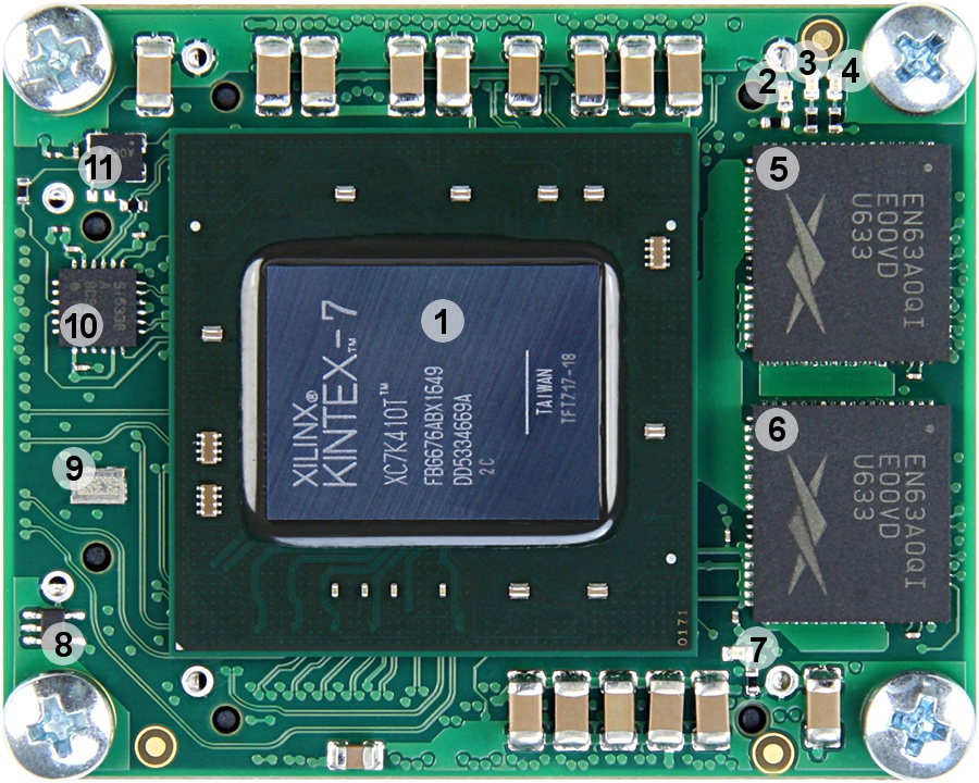
Figure 2.1: TE0741--03-410-2CF module.

Figure 2.2: TE0741-03-160-2C1 module.
- Xilinx Kintex-7 FPGA, U1
- Green LED (DONE), D3
- Red LED (LED1), D2
- Green LED (LED2), D1
- EN63A0QI Voltage Regulator 1.0V (Master), U14
- EN63A0QI Voltage Regulator 1.0V (Slave), U15
- Green LED (C_LED), D4
Voltage detector, U11
- Serial number (traceability) pad
- I2C-programmable any-frequency, any-output quad clock generator, U2
- Low-power programmable oscillator @ 25.000000 MHz, U3
- Samtec Razor Beam™ LSHM-150 B2B connector, JM2
- 32 MByte quad SPI Flash memory, U4
- Samtec Razor Beam™ LSHM-130 B2B connector, JM3
- 3A PFET load switch with configurable slew rate (3.3V), Q1
- Samtec Razor Beam™ LSHM-150 B2B connector, JM1
- System Controller CPLD, U7
- EP53F8QI Voltage Regulator (1.2V_MGT), U6
- EP53F8QI Voltage Regulator (1.8V), U8
- EP53F8QI Voltage Regulator (1V_MGT), U16
Initial Delivery State
| Storage device name | Content | Notes |
|---|---|---|
SPI Flash OTP Area | Empty, not programmed | Except serial number programmed by flash vendor. |
SPI Flash Quad Enable bit | Programmed | - |
SPI Flash main array | Demo design | - |
eFUSE USER | Not programmed | - |
eFUSE Security | Not programmed | - |
Table 1: Initial delivery state.
Signals, Interfaces and Pins
Board to Board (B2B) I/Os
Overview of the I/O signal banks connected to the B2B connectors:
| Bank | Type | B2B Connector | I/O Signal Count | Voltage | Notes |
|---|---|---|---|---|---|
0 | HR | - | - | 3.3V | Configuration bank. |
12 | HR | JM2 | 50 I/Os, 24 LVDS pairs | User | Supported voltage level from 1.2V to 3.3V. NOTE: BANK 12 IS NOT AVAILABLE ON THE K70T DEVICE! |
13 | HR | JM1 | 48 I/Os, 24 LVDS pairs | User | Supported voltage level from 1.2V to 3.3V. |
14 | HR | JM1 JM3 | 8 I/Os 4 I/Os, 2 LVDS pairs | 3.3V | IO pins at B2B connector JM1, support only 3.3V. |
15 | HR | JM2 | 18 I/Os, 9 LVDS pairs | User | Supported voltage level from 1.2V to 3.3V. |
16 | HR | JM3 | 16 I/Os, 8 LVDS pairs | User | Supported voltage level from 1.2V to 3.3V. |
32 | HP | NC | - | - | Bank not used. |
33 | HP | NC | - | - | Bank not used. |
| 34 | HP | NC | - | - | Bank not used. |
Table 2: Available I/O signal banks connected to the B2B connectors.
Please use Master Pin-out Table table as primary reference for the pin mapping information.
JTAG Interface
JTAG access to the Xilinx Kintex-7 and to the System Controller CPLD is provided through B2B connector JM2.
| JTAG Signal | B2B Connector |
|---|---|
| TMS | JM2-93 |
| TDI | JM2-95 |
| TDO | JM2-97 |
| TCK | JM2-99 |
Table 3: Pin-mapping of JTAG Interface on B2B connector.
JTAGMODE pin 89 in B2B connector JM1 is used to select which device is accessible, low - Xilinx Kintex-7, high - System Controller CPLD.
System Controller I/O Pins
Special purpose pins are connected to smaller System Controller CPLD and have following default configuration:
| Pin Name | Mode | Function | Default Configuration | B2B Connector |
|---|---|---|---|---|
| PGOOD | Output | Power Good | Active high when all on-module power supplies are working properly. | JM1-30 |
| RESIN | Input | Reset | Active low reset signal, drive low to keep the system in reset (FPGA pin PROG_B will be driven by CPLD). | JM2-18 |
| JTAGMODE | Input | JTAG Select | Low for normal operation, high (3.3V) to program the System Controller CPLD. | JM1-89 |
Table 4: Pin-description of System Controller CPLD.
On-board LEDs
There are four LED's available on TE0741 SoM. Two status LED's (D3 and D4) and two user configurable LED's (D1 and D2).
| LED | Color | Connected to | Description and Notes |
|---|---|---|---|
| D1 | Green | LED2 | User configurable LED. |
| D2 | Red | LED1 | User configurable LED. |
| D3 | Green | DONE | Reflects inverted DONE signal, ON when FPGA is not configured, OFF as soon as PL is configured. This LED will not operate if the the 3.3V power rail is not available. After FPGA configuration the user can use USRACCESSE2 to control Done LED. |
| D4 | Green | C_LED | Connected to the system controller indicating status of the module: Steadily lit: RESIN pin is kept low. Blinking fast (0.1s on/off): Power sequencing fault (PG_ALL = 0). Blinking at medium speed (0.5s on/off): Power sequencing has completed but the FPGA is not configured (PG_ALL = 1, DONE = 0). Blinking slow (1s on/off): FPGA is configured and board is ready (PG_ALL = 1, DONE = 1). It is also possible to program the System Controller CPLD to connect this LED to FPGA pin named XIO. |
Table 5: Description of the on board LED's.
Note: if FPGA logic toggles DONE pin (to control D3) then D4 will toggle at random, as changing value on DONE will change the blink frequency of D4.
DONE LED will be ON as long as FPGA is NOT configured and will be OFF when FPGA is configured successfully. If user STARTUPE2 primitive is used in user design then DONE LED is controlled by the user design and can be on/off/blink or have any other functionality defined by the user.
Clocking
To enable the PLL (phase-locked loop) clock generator Si5338A (U2), CLK_EN-signal (bank 14, pin C26) must be set to high, to activate the 25 MHz reference clock SiT8208AI (U3). The GTX reference clocks 0 and 2 have to be provided by the user on B2B connector JM3.
| Clock | Frequency | IC | FPGA | Notes |
|---|---|---|---|---|
PLL reference | 25 MHz | U3 SiT8208AI | - | Activated by CLK_EN pin of FPGA. |
GTX REFCLK0 | - | B2B | D5/D6 | B2B connector pins: MGT_CLK_0_N: JM3-31 MGT_CLK_0_P: JM3-33 Needs decoupling and differential terminator on base board. |
| GTX REFCLK1 | 125 MHz | U2 Si5338 | F5/F6 | PLL clock 1, default frequency is 125 MHz. |
| GTX REFCLK2 | - | B2B | H5/H6 | B2B connector pins: MGT_CLK_2_N: JM3-32 MGT_CLK_2_P: JM3-34 Needs decoupling and differential terminator on base board. |
| GTX REFCLK3 | 125 MHz | U2 Si5338 | K5/K6 | PLL clock 2, default not configured |
| Bank 14 input clock | 100 MHz | U2 Si5338 | F22/E23 | PLL clock 0, default frequency is 100 MHz. |
Table 6: Clocks overview.
On-board Peripherals
Programmable PLL Clock (Phase-Locked Loop)
There is a Silicon Labs I2C programmable clock generator Si5338A (U2) chip on the module. It's output frequencies can be programmed using the I2C bus address 0x70 or 0x71 (PLL_IN4 (LSB of I2C-Address) must be set for address 0x71).
A 25 MHz oscillator is connected to pin IN3 and is used to generate the output clocks. The oscillator has its enable pin connected to an FPGA pin (CLK_EN). Driving the FPGA pin low will disable the oscillator output, setting it high will enable it. Three of the Si5338 clock outputs are connected to the FPGA. One is connected to a logic bank and the other two are connected to the GTX banks. It is possible to use the clocks connected to the GTX bank in the user's logic design. This is achieved by instantiating a IBUFDSGTE buffer in the design.
The default frequency of each clock at start up is detailed in the table 7.
Once running, the frequency and other parameters can be changed by programming the device using the I2C bus connected between the FPGA (master) and clock generator (slave). Logic needs to be generated inside the FPGA to utilize I2C bus correctly.
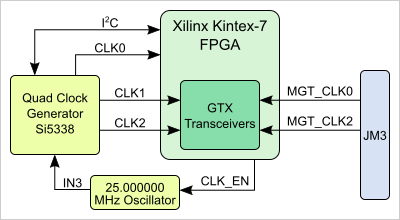
Figure 3: Clocking block diagram.
| I/O Si5338A (U2) | Default Frequency | Notes |
|---|---|---|
IN1/IN2 | - | Not used (external clock signal supply). |
IN3 | 25MHz | Fixed input clock signal from. reference clock generator SiT8208AI (U3). |
IN4 | - | LSB of the default I2C-Adress 0x70. |
IN5/IN6 | - | Not used (external clock signal supply). |
CLK0 A/B | 100 MHz | Bank 14 clock input, Pins: B14_L12_P, B14_L12_N |
CLK1 A/B | 125MHz | MGT reference clock 1 to FPGA Bank 116 MGT |
CLK2 A/B | - | MGT reference clock 3 to FPGA Bank 115 MGT |
| CLK3 | - | not used |
Table 7: Pin description of Si5338A PLL clock generator.
32 MByte Quad SPI Flash Memory
An SPI flash memory S25FL256SAGBHI20 (U4) is provided for FPGA configuration file storage. After configuration completes the remaining free memory can be used for application data storage. All four SPI data lines are connected to the FPGA allowing x1, x2 or x4 data bus widths to be used. The maximum data transfer rate depends on the bus width and clock frequency.
SPI Flash QE (Quad Enable) bit must be set, or the FPGA would not configure itself from Flash. This bit is always set at the manufacturing.
GTX Transceivers
The Kintex-7 device that is used on the TE0741 board has 8 GTX transceivers. All 8 are wired directly to connectors JM1 and JM3. There are also 4 clocks that are associated with the transceivers. Two of the clocks are connected directly to JM3, whilst the other two are derived from the clock generator. As there is no capacitive coupling of the data and clock lines that are connected to the connectors, these may be required on the user’s PCB depending on the application.
To enable the voltage supply for the GTX transceivers, namely the Enpirion EP53F8QI voltage regulators U6 and U16, which serve the voltages MGTAVCC (1.0 V) and MGTAVTT (1.2 V), the signal EN_MGT (bank 14, pin H22) have to be set high. The voltage regulators will indicate "Power OK" with signals PG_MGT_1V and PG_MGT_1V2, when reaching stable state.
![]()
Figure 4: GTX transceiver block diagram.
System Controller CPLD
The System Controller CPLD is used to coordinate the configuration of the FPGA. The FPGA is held in reset (by driving the PROG_B signal) until the power supplies have sequenced. Setting input signal RESIN low will also reset the FPGA. This signal can be driven from the user’s PCB via the board connector.
User can create its own System Controller CPLD design using the Lattice Diamond software and program it into the device using the JTAG interface. The JTAGMODE signal should be set to 3.3V to enable programming mode, for normal module operation it should be set to 0V.
Green LED D4 (C_LED) connected to the System Controller CPLD is to indicate the status of the module.
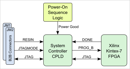
Figure 5: System Controller CPLD block diagram.
Power and Power-On Sequence
Power Supply
Power supply with minimum current capability of 3A for system startup is recommended.
Power Consumption
| Power Input Pin | Typical Current |
|---|---|
| VIN | TBD* |
| 3.3VIN | TBD* |
Table 8: Maximum current of power supplies.
* TBD - To Be Determined.
Lowest power consumption is achieved when powering the module from single 3.3V supply. When using split 3.3V/5V power supplies, the power consumption (and heat dissipation) will rise, this is due to the DC-DC converter efficiency (it decreases when VIN/VOUT ratio rises).
Power-On Sequence
For highest efficiency of on board DC-DC regulators, it is recommended to use same 3.3V power source for both VIN and 3.3VIN power rails. Although VIN and 3.3VIN can be powered up in any order, it is recommended to power them up simultaneously.
It is important that all baseboard I/Os are 3-stated at power-on until System Controller sets PGOOD signal high (B2B connector JM1, pin 30), or 3.3V is present on B2B connector JM2 pins 10,12 or 91, meaning that all on-module voltages have become stable and module is properly powered up.
See Xilinx datasheet DS182 for additional information. User should also check related baseboard documentation when choosing baseboard design for TE0741 module.
The FPGA 1.0V supply is derived from two regulators operating in a parallel allowing higher load currents. To start the power-on sequence, pin EN1 (JM1-28, enable 1.0V voltage regulators) is by default high. By driving EN1 pin low on base-board the power-on sequence will not start until the EN1 pin is released to high.
Power Rails
Voltages on B2B-Connectors | B2B JM1 Pin | B2B JM2 Pin | B2B Direction | Note |
|---|---|---|---|---|
| VIN | 1, 3, 5 | 2, 4, 6, 8 | Input | Supply voltage. |
| 3.3VIN | 13, 15 | - | Input | Supply voltage. |
| VCCIO12 | - | 7, 9 | Input | High range bank voltage. |
| VCCIO13 | 9, 11 | - | Input | High range bank voltage. |
| VCCIO15 | - | 5 | Input | High range bank voltage. |
| VCCIO16 | - | 1, 3 | Input | High range bank voltage. |
| 3.3V | - | 10, 12, 91 | Output | Internal 3.3V voltage level. |
Table 9: Power rails of SoM on B2B connectors.
Bank Voltages
| Bank | Schematic Name | Voltage | Range |
|---|---|---|---|
| 0 Config | 3.3V | 3.3V | - |
| 12 | VCCIO12 | user | HR: 1.2V to 3.3V |
| 13 | VCCIO13 | user | HR: 1.2V to 3.3V |
| 14 | 3.3V | 3.3V | - |
| 15 | VCCIO15 | user | HR: 1.2V to 3.3V |
| 16 | VCCIO16 | user | HR: 1.2V to 3.3V |
Table 10: Range of FPGAs bank voltages.
See Xilinx Kintex-7 datasheet DS182 for the voltage ranges allowed.
Board to Board Connectors
Unable to render {include} The included page could not be found.
Variants Currently In Production
Module Variant | FPGA | U15 | FPGA Junction Temperature | Temperature Grade |
|---|---|---|---|---|
| TE0741-03-070-2CF | XC7K70T-2FBG676C | - | 0°C to 85°C | Commercial grade |
| TE0741-03-070-2IF | XC7K70T-2FBG676I | - | -40°C to 100°C | Industrial grade |
| TE0741-03-160-2CF | XC7K160T-2FBG676C | - | 0°C to 85°C | Commercial grade |
| TE0741-03-160-2C1 | XC7K160T-2FFG676C | - | 0°C to 85°C | Commercial grade |
| TE0741-03-160-2IF | XC7K160T-2FBG676I | - | -40°C to 100°C | Industrial grade |
| TE0741-03-325-2CF | XC7K325T-2FBG676C | EN63A0QI | 0°C to 85°C | Commercial grade |
| TE0741-03-325-2IF | XC7K325T-2FBG676I | EN63A0QI | -40°C to 100°C | Industrial grade |
| TE0741-03-410-2CF | XC7K325T-2FBG676C | EN63A0QI | 0°C to 85°C | Commercial grade |
Table 11: Module TE0741-03 variants.
Technical Specifications
Absolute Maximum Ratings
| Parameter | Min | Max | Units | Notes |
|---|---|---|---|---|
VIN supply voltage | -0.3 | 6.5 | V | - |
| 3.3VIN supply voltage | -0.1 | 3.6 | V | - |
| PL IO bank supply voltage for HR I/O banks (VCCO) | -0.5 | 3.6 | V | - |
| I/O input voltage for HR I/O banks | -0.4 | VCCO_X+0.55 | V | - |
| GT receiver (RXP/RXN) and transmitter (TXP/TXN) | -0.5 | 1.26 | V | Xilinx datasheet DS182 |
| Voltage on module JTAG pins | -0.5 | VCCO_0+0.45 | V | VCCO_0 is 3.3V nominal. |
| Storage temperature | -55 | +125 | °C | - |
Table 12: Absolute maximum ratings.
Recommended Operating Conditions
| Parameter | Min | Max | Units | Notes | Reference Document |
|---|---|---|---|---|---|
| VIN supply voltage | 2.4 | 5.5 | V | - | EP53F8QI data sheet |
| 3.3VIN supply voltage | 3.135 | 3.465 | V | 3,3V ± 5% | - |
| PL I/O bank supply voltage for HR I/O banks (VCCO) | 1.14 | 3.465 | V | - | Xilinx datasheet DS182 |
| I/O input voltage for HR I/O banks | -0.20 | VCCO+0.2 | V | - | Xilinx datasheet DS182 |
| GT receiver (RXP/RXN) and transmitter (TXP/TXN) | (*) | (*) | - | - | * See datasheet DS182 |
| Voltage on module JTAG pins | 3.135 | 3.465 | V | - | - |
Table 13: Recommended operation conditions.
Operating Temperature Ranges
Commercial grade: 0°C to +70°C.
Industrial grade: -40°C to +85°C.
The module operating temperature range depends also on customer design and cooling solution. Please contact us for options.
Check Xilinx datasheet DS182 for complete list of absolute maximum and recommended operating ratings.
Physical Dimensions
- Module size: 50 mm × 40 mm
- Mating height with standard connectors: 8mm
- PCB thickness: 1.6mm
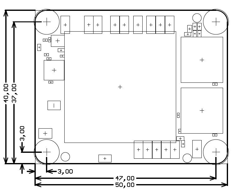
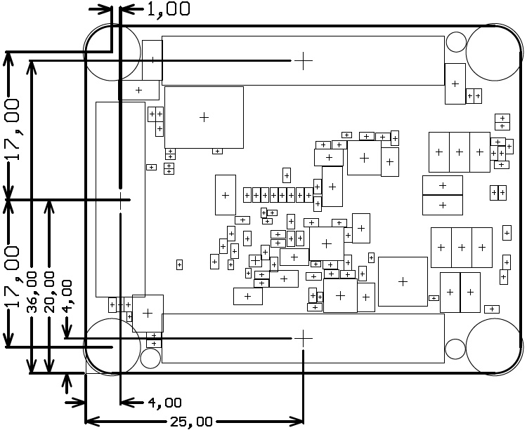
Figure 6: Physical dimensions of the TE0741 module. All dimensions are shown in millimeters.
Weight
19 g - Plain module.
8.8 g - Set of nuts and bolts.
Revision History
Hardware Revision History
| Date | Revision | Notes | PCN | Documentation |
|---|---|---|---|---|
| 2016-10-25 | 03 | 1) Fixed DC-DC connection for parallel operation 2) Samtec Razor Beam connectors updated 3) Serial number (traceability) pad added 4) Changed ferrite beads L1..L4 size 0402 to BKP0603HS121-T 5) Thermal vias added to mounting holes | PCN-20170106 | TE0741-03 |
| 2013-11-06 | 02 |
| TE0741-02 | |
| 01 | First production release |
Hardware revision number is written on the PCB board together with the module model number separated by the dash.


Figure 7: TE0741 PCB revision number.
Document Change History
| Date | Revision | Contributors | Description |
|---|---|---|---|
| Jan Kumann | New power-on diagram. Few improvements. Template revision added. | ||
| 2017-07-20 | v.57 | John Hartfiel | Correction: PLL default output CLKs. |
| 2017-06-07 | v.55 | Jan Kumann | Minor formatting |
| 2017-06-02 | v.50 | Jan Kumann | REV03 specific update. |
| 2017-01-22 | v.42 | Jan Kumann | New block diagram added. |
| 2017-01-13 | v.38 | Jan Kumann | New product images and physical dimension drawings. Formatting improvements and small corrections. |
| 2017-01-12 | v.21 | John Hartfiel | Correction: B2B and FPGA bank location. |
| 2016-12-14 | v.19 | Ali Naseri | TRM revision. |
| 2013-12-02 | v.1 | Antti Lukats, Jon Bean | Initial version. |
Disclaimer
Data Privacy
Please also note our data protection declaration at https://www.trenz-electronic.de/en/Data-protection-Privacy
Document Warranty
The material contained in this document is provided “as is” and is subject to being changed at any time without notice. Trenz Electronic does not warrant the accuracy and completeness of the materials in this document. Further, to the maximum extent permitted by applicable law, Trenz Electronic disclaims all warranties, either express or implied, with regard to this document and any information contained herein, including but not limited to the implied warranties of merchantability, fitness for a particular purpose or non infringement of intellectual property. Trenz Electronic shall not be liable for errors or for incidental or consequential damages in connection with the furnishing, use, or performance of this document or of any information contained herein.
Limitation of Liability
In no event will Trenz Electronic, its suppliers, or other third parties mentioned in this document be liable for any damages whatsoever (including, without limitation, those resulting from lost profits, lost data or business interruption) arising out of the use, inability to use, or the results of use of this document, any documents linked to this document, or the materials or information contained at any or all such documents. If your use of the materials or information from this document results in the need for servicing, repair or correction of equipment or data, you assume all costs thereof.
Copyright Notice
No part of this manual may be reproduced in any form or by any means (including electronic storage and retrieval or translation into a foreign language) without prior agreement and written consent from Trenz Electronic.
Technology Licenses
The hardware / firmware / software described in this document are furnished under a license and may be used /modified / copied only in accordance with the terms of such license.
Environmental Protection
To confront directly with the responsibility toward the environment, the global community and eventually also oneself. Such a resolution should be integral part not only of everybody's life. Also enterprises shall be conscious of their social responsibility and contribute to the preservation of our common living space. That is why Trenz Electronic invests in the protection of our Environment.
REACH, RoHS and WEEE
REACH
Trenz Electronic is a manufacturer and a distributor of electronic products. It is therefore a so called downstream user in the sense of REACH. The products we supply to you are solely non-chemical products (goods). Moreover and under normal and reasonably foreseeable circumstances of application, the goods supplied to you shall not release any substance. For that, Trenz Electronic is obliged to neither register nor to provide safety data sheet. According to present knowledge and to best of our knowledge, no SVHC (Substances of Very High Concern) on the Candidate List are contained in our products. Furthermore, we will immediately and unsolicited inform our customers in compliance with REACH - Article 33 if any substance present in our goods (above a concentration of 0,1 % weight by weight) will be classified as SVHC by the European Chemicals Agency (ECHA).
RoHS
Trenz Electronic GmbH herewith declares that all its products are developed, manufactured and distributed RoHS compliant.
WEEE
Information for users within the European Union in accordance with Directive 2002/96/EC of the European Parliament and of the Council of 27 January 2003 on waste electrical and electronic equipment (WEEE).
Users of electrical and electronic equipment in private households are required not to dispose of waste electrical and electronic equipment as unsorted municipal waste and to collect such waste electrical and electronic equipment separately. By the 13 August 2005, Member States shall have ensured that systems are set up allowing final holders and distributors to return waste electrical and electronic equipment at least free of charge. Member States shall ensure the availability and accessibility of the necessary collection facilities. Separate collection is the precondition to ensure specific treatment and recycling of waste electrical and electronic equipment and is necessary to achieve the chosen level of protection of human health and the environment in the European Union. Consumers have to actively contribute to the success of such collection and the return of waste electrical and electronic equipment. Presence of hazardous substances in electrical and electronic equipment results in potential effects on the environment and human health. The symbol consisting of the crossed-out wheeled bin indicates separate collection for waste electrical and electronic equipment.
Trenz Electronic is registered under WEEE-Reg.-Nr. DE97922676.
Overview
Content Tools