Page History
...
- Xilinx Zynq UltraScale+ MPSoC (XCZU2CG / XCZU2EG, XCZU3CG / XCZU3EG or XCZU4CG / XCZU4EV)
- Quad-core or dual-core Cortex-A53 64-bit ARM v8 application processing unit (APU) (depends on assembly variant CG,EG,EV)
- Dual Cortex-R5 32-bit ARM v7 real-time processing unit (RPU)
Four high-speed serial I/O (HSSIO) interfaces supporting following protocols:
- PCI Express® interface version 2.1 compliant
- SATA 3.1 specification compliant interface
DisplayPort source-only interface with video resolution up to 4k x 2k
- USB 3.0 specification compliant interface implementing a 5 Gbit/s line rate
- 1 GB/s serial GMII interface
- 132 x HP PL I/Os (3 banks)
- 14 x PS MIOs (6 of the MIOs intended for SD card interface in default configuration)
- 4 x serial PS GTR transceivers
- 2 GByte DDR4 SDRAM, 32bit databus-width
- 128 MByte QSPI boot Flash in dual parallel mode
- 4 GByte eMMC
- Programmable quad PLL clock generator PLL for PS GTR clocks (optional external reference)
- Gigabit Ethernet transceiver PHY (Marvell Alaska 88E1512)
- MAC address serial EEPROM with EUI-48™ node identity (Microchip 24AA025E48)
- Hi-speed USB2 ULPI transceiver with full OTG support (Microchip USB3320C)
- Plug-on module with 2 x 100-pin and 1 x 60-pin high-speed hermaphroditic strips
- All power supplies on board
- Size: 50 x 40 mm
...
| Storage Device Name | Content | Notes |
|---|---|---|
SPI Flash OTP Area | Empty, not programmed | Except serial number programmed by flash vendor. |
SPI Flash Quad Enable bit | Programmed | - |
SPI Flash main array | Not programmed | - |
eFUSE USER | Not programmed | - |
eFUSE Security | Not programmed | - |
| Si5338 OTP NVM | Not programmed | - |
| CPLD (LCMXO2-256HC) | SC0820-02 QSPI Firmware | See Boot Process section. |
Table 1: Initial delivery state of programmable devices on the module
...
Zynq MPSoC's I/O banks signals connected to the B2B connectors:
| Bank | Type | B2B Connector | I/O Signal Count | Voltage | Notes |
|---|---|---|---|---|---|
64 | HP | JM2 | 48 | User | Max voltage 1.8V |
64 | HP | JM2 | 2 | User | Max voltage 1.8V |
| 65 | HP | JM2 | 18 | User | Max voltage 1.8V |
65 | HP | JM3 | 16 | User | Max voltage 1.8V |
66 | HP | JM1 | 48 | User | Max voltage 1.8V |
| 500 | MIO | JM1 | 8 | 1.8V | - |
501 | MIO | JM1 | 6 | 3.3V | - |
505 | GTR | JM3 | 4 lanes | - | - |
505 | GTR CLK | JM3 | 1 differential input | - | - |
Table 3: General overview of board to board I/O signals
For detailed information about the pin-out, please refer to the Pin-out table.
MGT Lanes
The Xilinx Zynq UltraScale+ device used on the TE0820 module has 4 GTR transceivers. All 4 are wired directly to B2B connector JM3. MGT (Multi Gigabit Transceiver) lane consists of one transmit and one receive (TX/RX) differential pairs, four signals total per one MGT lane. Following table lists lane number, FPGA bank number, transceiver type, signal schematic name, board-to-board pin connection and FPGA pins connection:
...
| Pin Name | Mode | Function | Default Configuration |
|---|---|---|---|
| EN1 | Input | Power Enable | No hard wired function on PCB. When forced low, pulls up PGOOD, goes low without effect on power management. |
| PGOOD | Output | Power Good | Active high when all on-module power supplies are working properly. |
| NOSEQ | - | - | No function. |
| RESIN | Input | Reset | Active low reset, gated to POR_B. |
| JTAGEN | Input | JTAG Select | Low for normal operation, high for CPLD JTAG access. |
Table 7: System Controller CPLD special purpose pins.
See also TE0820-REV01_REV02 CPLD
Default PS MIO Mapping
| PS MIO | Function | B2B Pin | Connected to | PS MIO | Function | B2B Pin | Connected to |
|---|---|---|---|---|---|---|---|
| 0 | SPI0 | - | U7-B2, CLK | 40..45 | - | - | Not connected |
| 1 | SPI0 | - | U7-D2, DO/IO1 | 46 | SD | JM1-17 | B2B, SD_DAT3 |
| 2 | SPI0 | - | U7-C4, WP/IO2 | 47 | SD | JM1-19 | B2B, SD_DAT2 |
| 3 | SPI0 | - | U7-D4, HOLD/IO3 | 48 | SD | JM1-21 | B2B, SD_DAT1 |
| 4 | SPI0 | - | U7-D3, DI/IO0 | 49 | SD | JM1-23 | B2B, SD_DAT0 |
| 5 | SPI0 | - | U7-C2, CS | 50 | SD | JM1-25 | B2B, SD_CMD |
| 6 | N/A | - | Not connected | 51 | SD | JM1-27 | B2B, SD_CLK |
| 7 | SPI1 | - | U17-C2, CS | 52 | USB_PHY | - | U18-31, OTG-DIR |
| 8 | SPI1 | - | U17-D3, DI/IO0 | 53 | USB_PHY | - | U18-31, OTG-DIR |
| 9 | SPI1 | - | U17-D2, DO/IO1 | 54 | USB_PHY | - | U18-5, OTG-DATA2 |
| 10 | SPI1 | - | U17-C4, WP/IO2 | 55 | USB_PHY | - | U18-2, OTG-NXT |
| 11 | SPI1 | - | U17-D4, HOLD/IO3 | 56 | USB_PHY | - | U18-3, OTG-DATA0 |
| 12 | SPI1 | - | U17-B2, CLK | 57 | USB_PHY | - | U18-4, OTG-DATA1 |
| 13..20 | eMMC | - | U6, MMC-D0..D7 | 58 | USB_PHY | - | U18-29, OTG-STP |
| 21 | eMMC | - | U6, MMC-CMD | 59 | USB_PHY | - | U18-6, OTG-DATA3 |
| 22 | eMMC | - | U6, MMC-CLKR | 60 | USB_PHY | - | U18-7, OTG-DATA4 |
| 23 | eMMC | - | U6, MMC-RST | 61 | USB_PHY | - | U18-9, OTG-DATA5 |
| 24 | ETH | - | U8, ETH-RST | 62 | USB_PHY | - | U18-10, OTG-DATA6 |
| 25 | USB_PHY | - | U18, OTG-RST | 63 | USB_PHY | - | U18-13, OTG-DATA7 |
| 26 | MIO | JM1-95 | B2B, as PJTAG MIO possible | 64 | ETH | - | U8-53, ETH-TXCK |
| 27 | MIO | JM1-93 | B2B, as PJTAG MIO possible | 65..66 | ETH | - | U8-50..51, ETH-TXD0..1 |
| 28 | MIO | JM1-99 | B2B, as PJTAG MIO possible | 67..68 | ETH | - | U8-54..55, ETH-TXD2..3 |
| 29 | MIO | JM1-99 | B2B, as PJTAG MIO possible | 69 | ETH | - | U8-56, ETH-TXCTL |
| 30 | MIO | JM1-92 | B2B (UART RX) | 70 | ETH | - | U8-46, ETH-RXCK |
| 31 | MIO | JM1-85 | B2B (UART TX) | 71..72 | ETH | - | U8-44..45, ETH-RXD0..1 |
| 32 | MIO | JM1-91 | B2B | 73..74 | ETH | - | U8-47..48, ETH-RXD2..3 |
| 33 | MIO | JM1-87 | B2B | 75 | ETH | - | U8-43, ETH-RXCTL |
| 34..37 | - | - | Not connected | 76 | ETH | - | U8-7, ETH-MDC |
| 38 | I2C | - | U10-12, SCL | 77 | ETH | - | U8-8, ETH-MDIO |
| 39 | I2C | - | U10-19, SDA | - | - | - | - |
Table 8: TE0820-02 PS MIO mapping
...
See also TE0820 System Controller CPLD page.
eMMC Flash Memory
eMMC Flash memory device(U6) is connected to the ZynqMP PS MIO bank 500 pins MIO13..MIO23. eMMC chips MTFC4GACAJCN-4M IT (FLASH - NAND Speicher-IC 32 Gb (4 G x 8) MMC ) is used.
...
| Signal | Frequency | Notes | |
|---|---|---|---|
| IN1/IN2 | - | user | External Not used (external clock signal supply ).from B2B connector JM3, pins JM3-32/JM3-34 |
IN3 | 25.000000 MHz | Fixed input clock signal from reference clock generator SiT8008BI-73-18S-25.000000E (U11). | |
| IN4 | - | LSB of the default I2C address, wired to ground mean address is 0x70. | |
IN5 | - | Not connected. | |
IN6 | - | Wired to ground. | |
| CLK0 A/B | - | Bank 65 clock input, pins K9 and J9. | |
CLK1 A/B | - | MGT reference clock 3 to FPGA Bank 505 MGT.PS GTR | |
CLK2 A/B | - | MGT reference clock 1 to FPGA Bank 505 MGT.PS GTR | |
| CLK3 A/B | - | Not connected. |
Table 12: General overview of the on-board quad clock generator I/O signals
...
| Scroll Title | ||||||||||||||||||||||||||||||||
|---|---|---|---|---|---|---|---|---|---|---|---|---|---|---|---|---|---|---|---|---|---|---|---|---|---|---|---|---|---|---|---|---|
| ||||||||||||||||||||||||||||||||
|
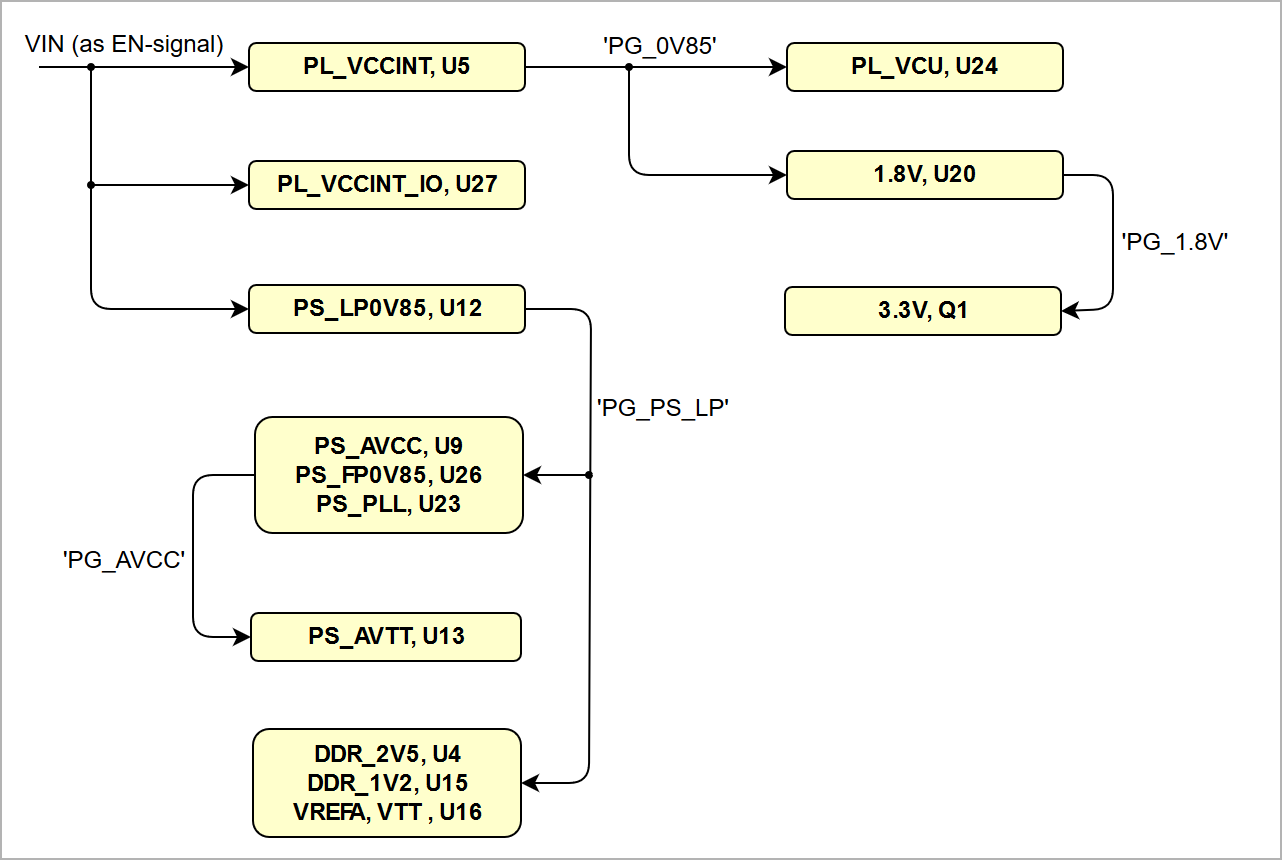
Figure 4: TE0820-03 power-on sequence diagram.
...
| Power Rail Name on B2B Connector | JM1 Pins | JM2 Pins | Direction | Notes |
|---|---|---|---|---|
| VIN | 1, 3, 5 | 2, 4, 6, 8 | Input | Supply voltage from the carrier board. |
| 3.3V | - | 10, 12 | Output | Internal 3.3V voltage level. |
| 3.3VIN | 13, 15 | - | Input | Supply voltage from the carrier board. |
| 1.8V | 39 | - | Output | Internal 1.8V voltage level. |
| JTAG VREF | - | 91 | Output | JTAG reference voltage. Attention: Net name on schematic is "3.3VIN" |
| VCCO_64 | - | 7, 9 | Input | High performance I/O bank voltage. |
| VCCO_65 | - | 5 | Input | High performance I/O bank voltage. |
| VCCO_66 | 9, 11 | - | Input | High performance I/O bank voltage. |
Table 16: TE0820-02 power rails
...
| Bank | Name on Schematic | Voltage | Range |
|---|---|---|---|
| 64 HP | VCCO_64 | User | HP: 1.0V to 1.8V |
| 65 HP | VCCO_65 | User | HP: 1.0V to 1.8V |
| 66 HP | VCCO_66 | User | HP: 1.0V to 1.8V |
| 500 PSMIO | VCCO_PSIO0_500 | 1.8V | - |
| 501 PSMIO | VCCO_PSIO1_501 | 3.3V | - |
| 502 PSMIO | VCCO_PSIO2_502 | 1.8V | - |
| 503 PSCONFIG | VCCO_PSIO3_503 | 1.8V | - |
| 504 PSDDR | VCCO_PSDDR_504 | 1.2V | - |
...
Technical Specifications
Absolute Maximum Ratings
Parameter | Min | Max | Units | Notes |
|---|---|---|---|---|
VIN supply voltage | -0.3 | 7 | V | See EN6347QI and TPS82085SIL datasheets |
| 3.3VIN supply voltage | -0.1 | 3.630 | V | Xilinx DS925 and TPS27082L datasheet |
| PS I/O supply voltage, VCCO_PSIO | -0.5 | 3.630 | V | Xilinx document DS925 |
| PS I/O input voltage | -0.5 | VCCO_PSIO + 0.55 | V | Xilinx document DS925 |
| HP I/O bank supply voltage, VCCO | -0.5 | 2.0 | V | Xilinx document DS925 |
| HP I/O bank input voltage | -0.55 | VCCO + 0.55 | V | Xilinx document DS925 |
| PS GTR reference clocks absolute input voltage | -0.5 |
| 1. |
| 1 | V |
| Xilinx document DS925 | ||||
| PS GTR absolute input voltage | -0.5 | 1.1 | V | Xilinx document DS925 |
Voltage on SC CPLD pins | -0.5 | 3.75 | V | Lattice Semiconductor MachXO2 datasheet |
Storage temperature | -40 | +85 | °C | See eMMC datasheet |
Table 18: Module absolute maximum ratings
Recommended Operating Conditions
| Parameter | Min | Max | Units | Notes |
|---|---|---|---|---|
| VIN supply voltage | 2.5 | 6 | V | See TPS82085S datasheet |
| 3.3VIN supply voltage | 2.375 | 3.465 | V | See LCMXO2-256HC, Xilinx DS925 datasheet |
| PS I/O supply voltage, VCCO_PSIO | 1.710 | 3.465 | V | Xilinx document DS925 |
| PS I/O input voltage | –0.20 | VCCO_PSIO + 0.20 | V | Xilinx document DS925 |
| HP I/O banks supply voltage, VCCO | 0.950 | 1.9 | V | Xilinx document DS925 |
| HP I/O banks input voltage | -0.20 | VCCO + 0.20 | V | Xilinx document DS925 |
| Voltage on SC CPLD pins | -0.3 | 3.6 | V | Lattice Semiconductor MachXO2 datasheet |
| Operating Temperature Range | 0 | 85 | °C | Xilinx document DS925, extended grade Zynq temperarure range |
Table 19: Recommended operating conditions
Module operating temperature range depends also on customer design and cooling solution. Please contact us for options.
| Note |
|---|
| See Xilinx datasheet DS925 for more information about absolute maximum and recommended operating ratings for the Zynq UltraScale+ chips. |
Operating Temperature Ranges
Extended grade: 0°C to +85°C.
Module operating temperature range depends also on customer design and cooling solution. Please contact us for options.
Physical Dimensions
Module size: 50 mm × 40 mm. Please download the assembly diagram for exact numbers.
Mating height with standard connectors: 8 mm
PCB thickness: 1.6 mm
Highest part on PCB: approximately 5 mm. Please download the step model for exact numbers.
...
Table 20: Hardware revision history table.
| Scroll Title | ||||
|---|---|---|---|---|
| ||||
|
...
Date | Revision | Contributors | Description | ||||||||||||||||||||||||
|---|---|---|---|---|---|---|---|---|---|---|---|---|---|---|---|---|---|---|---|---|---|---|---|---|---|---|---|
|
|
|
| ||||||||||||||||||||||||
| v.61 | John Hartfiel |
| |||||||||||||||||||||||||
| 2018-03-12 | v.54 |
| |||||||||||||||||||||||||
| 2017-11-20 | v.51 | John Hartfiel |
| ||||||||||||||||||||||||
| 2017-11-10 | v.50 | John Hartfiel |
| ||||||||||||||||||||||||
| 2017-10-18 | v.49 | John Hartfiel |
| ||||||||||||||||||||||||
| 2017-09-25 | v.48 | John Hartfiel |
| ||||||||||||||||||||||||
| 2017-09-18 | v.47 | John Hartfiel |
| ||||||||||||||||||||||||
| 2017-08-30 | v.46 | Jan Kumann |
| ||||||||||||||||||||||||
2017-08-24 | v.36 | John Hartfiel |
| ||||||||||||||||||||||||
| 2017-08-21 | v.34 | John Hartfiel |
| ||||||||||||||||||||||||
| 2017-08-21 | v.33 | Jan Kumann |
| ||||||||||||||||||||||||
| v.7 | John Hartfiel |
| ||||||||||||||||||||||||
2017-08-07 | v.5 | Jan Kumann | Initial version. |
Table 21: Document change history
...
Overview
Content Tools