Page History
...
The TEF1001 board offers two FAN connectors for cooling the FPGA device and on built-in FAN for the FMC modules.
| Connector | Schematic net names | Connected to | Notes |
|---|---|---|---|
| 4-Wire PWM FAN connector J4, 12V power supply | 'F1SENSE', pin 3 | SC CPLD U5, pin 99 | FPGA cooling FAN can be controlled via I²C interface from FPGA, see current SC CPLD firmware |
| 2-pin FAN connector J6, 5V power supply with TPS2051 Load Switch U25 | 'FAN_FMC_EN', U25 pin 4 | SC CPLD U5, pin 78 | FMC cooling FAN |
Table 9: FAN connectors
On-board Peripherals
...
| Si5338A Pin | Signal Name / Description | Connected to | Direction | Note |
|---|---|---|---|---|
IN1 | - | not connected | Input | not used |
| IN2 | - | GND | Input | not used |
IN3 | Reference input clock | U3, pin 3 | Input | 25.000000 MHz oscillator U14, Si8208AI |
IN4 | - | GND | Input | I2C slave device address LSB |
IN5 | - | not connected | Input | not used |
| IN6 | - | GND | Input | not used |
CLK0A | CLK0_P | U6, G24 | Output | -Clock to PL bank 14 |
| CLK0B | CLK0_N | U6, F24 | ||
| CLK1A | MGTCLK_5338_P | U6, G22H6 | Output | Clock to MGT bank 115, |
| CLK1B | MGTCLK_5338_N | U6, F23H5 | ||
| CLK2A | CLK1_P | U6, G22 | Output- | Clock to PL bank 14 |
| CLK2B | CLK1_N | U6, F23 | ||
| CLK3A | CLK2_P | U6, D23 | Output- | Clock to PL bank 14 |
| CLK3B | CLK2_N | U6, D24 |
Table 10: Programmable quad PLL clock generator inputs and outputs, *PCB REV01 is not programmed
Oscillators
The FPGA module has following reference clocking signals sources provided by external baseboard sources and on-board oscillators and FMC connector J2:
| Clock Source | Frequency | Signal Schematic Name | Clock Destination | Notes |
|---|---|---|---|---|
| U3U14, SiT8208AI | 25.000000 MHz | CLK | Si5338A PLL U2U13, pin 3 (IN3) | - |
| U11U1, DSC1123DL5 | 200.0000 MHz | CLK200MDDR3_CLK_P | FPGA bank 4533, pin R25AB11 | Enable by FPGA bank 65SC CPLD U5, pin AF2430 Signal: 'ENOSC200MHzCLK_EN' |
| CLK200MDDR3_CLK_N | FPGA bank 4533, pin R26 |
Table 11: Reference clock signals
On-board LEDs
...
Table 11: On-board LEDs
Power and Power-On Sequence
| HTML |
|---|
<!--
If power sequencing and distribution is not so much, you can join both sub sections together
--> |
Power Consumption
The maximum power consumption of a module mainly depends on the design running on the FPGA.
Xilinx provide a power estimator excel sheets to calculate power consumption. It's also possible to evaluate the power consumption of the developed design with Vivado. See also Trenz Electronic Wiki FAQ.
...
Table 12: Typical power consumption
* TBD - To Be Determined soon with reference design setup.
Single 3.3V power supply with minimum current capability of 4A for system startup is recommended.
For the lowest power consumption and highest efficiency of the on-board DC-DC regulators it is recommended to power the module from one single 3.3V supply. All input power supplies should have a nominal value of 3.3V. Although the input power supplies can be powered up in any order, it is recommended to power them up simultaneously.
| Warning |
|---|
| To avoid any damage to the module, check for stabilized on-board voltages should be carried out (i.e. power good and enable signals) before powering up any FPGA's I/O bank voltages VCCO_x. All I/Os should be tri-stated during power-on sequence. |
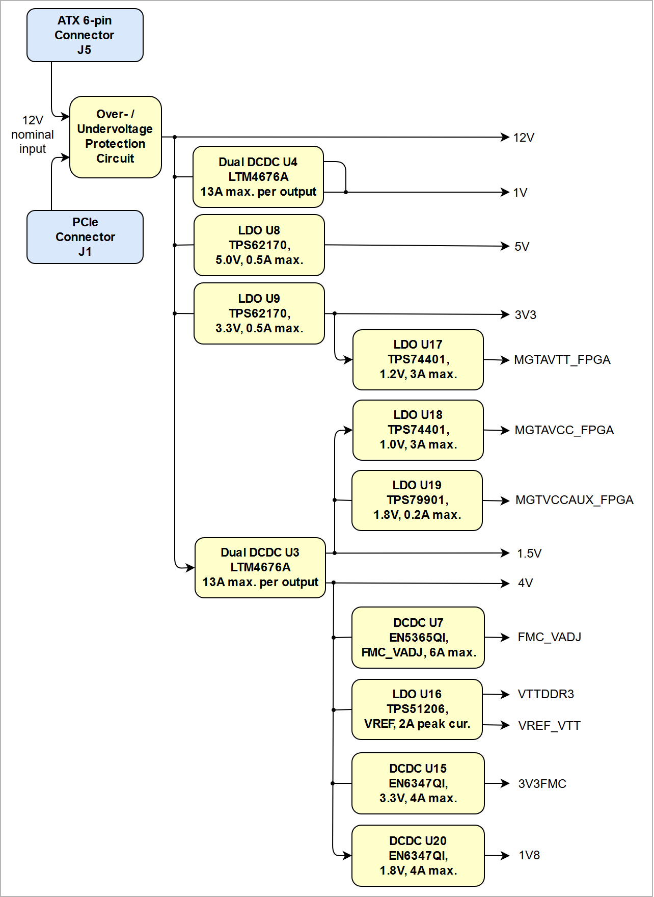
Power Distribution Dependencies
...
| anchor | Figure_3 |
|---|---|
| title | Figure 3: TEF1001-02 Power Distribution Diagram |
...
| Scroll Only |
|---|
|
Power-On Sequence
The TE0841 SoM meets the recommended criteria to power up the Xilinx FPGA properly by keeping a specific sequence of enabling the on-board DC-DC converters dedicated to the particular functional units of the FPGA chip and powering up the on-board voltages.
Following diagram clarifies the sequence of enabling the particular on-board voltages, which will power-up in descending order as listed in the blocks of the diagram:
...
| anchor | Figure_4 |
|---|---|
| title | Figure 4: TEF1001-02 Power-On Sequence Diagram |
...
| Scroll Only |
|---|
|
Power Rails
...
B2B JM1 Pins
...
B2B JM2 Pins
...
Input/Output
...
VBAT_IN
...
Table 13: Module power rails
Bank Voltages
...
Bank
...
Voltage
...
Voltage Range
...
PL_1.8V
...
1.8V
...
| AC11 | ||||
| FMC Connector J2 | - | GBTCLK0_M2C_P, Pin J2-D4 | FPGA bank 116, pin D6 | reference clock to MGT bank 116 |
| GBTCLK0_M2C_N, Pin J2-D5 | FPGA bank 116, pin D5 | |||
| - | GBTCLK1_M2C_P, Pin J2-B20 | FPGA bank 116, pin F6 | reference clock to MGT bank 116 | |
| GBTCLK1_M2C_N, Pin J2-B21 | FPGA bank 116, pin F5 | |||
| - | CLK0_M2C_P, Pin J2-H4 | FPGA bank 15, pin H17 | reference clock to PL bank 15 | |
| CLK0_M2C_N, Pin J2-H5 | FPGA bank 15, pin H18 | |||
| - | CLK1_M2C_P, Pin J2-G2 | FPGA bank 15, pin G17 | reference clock to PL bank 15 | |
| CLK1_M2C_N, Pin J2-G3 | FPGA bank 15, pin G18 | |||
| - | CLK2_BIDIR_P, Pin J2-K4 | FPGA bank 13, pin P23 | reference clock to PL bank 13 bidirectional clock line | |
| CLK2_BIDIR_N, Pin J2-K5 | FPGA bank 13, pin N23 | |||
| - | CLK3_BIDIR_P, Pin J2-J2 | FPGA bank 13, pin R22 | reference clock to PL bank 13 bidirectional clock line | |
| CLK3_BIDIR_N, Pin J2-J3 | FPGA bank 13, pin R23 |
Table 11: Reference clock signals
On-board LEDs
| LED | Color | Signal Schematic name | Connected to | Description and Notes |
|---|---|---|---|---|
| D1 | Green | FPGA_LED1_VT | FPGA bank 13, pin K25 | LEDs D1 to D10 are available to user. LED voltages are translated from bank voltage |
| D2 | Green | FPGA_LED2_VT | FPGA bank 13, pin K26 | |
| D3 | Green | FPGA_LED3_VT | FPGA bank 13, pin P26 | |
| D4 | Green | FPGA_LED4_VT | FPGA bank 13, pin R26 | |
| D5 | Green | FPGA_LED5_VT | FPGA bank 13, pin N16 | |
| D6 | Green | FPGA_LED6_VT | FPGA bank 14, pin J26 | |
| D7 | Green | FPGA_LED7_VT | FPGA bank 14, pin H26 | |
| D8 | Green | FPGA_LED8_VT | FPGA bank 14, pin E26 | |
| D9 | Green | FPGA_LED9_VT | FPGA bank 14, pin A24 | |
| D10 | Green | FPGA_LED10_VT | FPGA bank 15, pin F19 | |
| D11 | Green | LED1 | System Controller CPLD, bank 0, pin 76 | see current CPLD firmware for LED functionality |
Table 12: On-board LEDs
Configuration DIP-switch
There is one 4-bit DIP-witches S1 present on the TEB0911 board to configure options and set parameters. The following section describes the functionalities of the particular switches.
Table below describes the functionalities of the switches of DIP-switches S3 and S4 at their each positions:
| DIP-switch S3 | Signal Schematic Name | Connected to | Functionality | Notes |
|---|---|---|---|---|
| S1-1 | JTAG_EN | SC CPLD U5, bank 1, pin 82 | enables JTAG interface of SC CPLD U5 | SC CPLD programmable through JTAG connector, J8 |
| S1-2 | VID0_FMC_VADJ_CTRL | SC CPLD U5, bank 1, pin 71 | set 3-bit code to set FMC_VADJ voltage | The FMC_VADJ voltage is provided by DCDC U7 EN5365QI, the voltage can be set from 0.8V to 3.3V in 7 steps, see |
| S1-3 | VID1_FMC_VADJ_CTRL | SC CPLD U5, bank 1, pin 63 | ||
| S1-4 | VID2_FMC_VADJ_CTRL | SC CPLD U5, bank 1, pin 62 |
Table 13: DIP-switch S1 functionality description
Power and Power-On Sequence
| HTML |
|---|
<!--
If power sequencing and distribution is not so much, you can join both sub sections together
--> |
Power Consumption
The maximum power consumption of a module mainly depends on the design running on the FPGA.
Xilinx provide a power estimator excel sheets to calculate power consumption. It's also possible to evaluate the power consumption of the developed design with Vivado. See also Trenz Electronic Wiki FAQ.
| Power Input | Typical Current |
|---|---|
| 12V VIN | TBD* |
Table 14: Typical power consumption
* TBD - To Be Determined soon with reference design setup.
It is recommended to connect the ATX connector J5 to a 12V power supply source with minimum current capability of 6A to provide a sufficient power source to the board. Only one power source is needed at the same time, the system disconnects automatically PCIe power supply from PCIe edge connector J1 if the board is powered by the ATX connector J5.
| Warning |
|---|
| To avoid any damage to the module, check for stabilized on-board voltages should be carried out (i.e. power good and enable signals) before powering up any FPGA's I/O bank voltages VCCO_x. All I/Os should be tri-stated during power-on sequence. |
Power Distribution Dependencies
| Scroll Title | ||||||||||||||||||||||||||||||||
|---|---|---|---|---|---|---|---|---|---|---|---|---|---|---|---|---|---|---|---|---|---|---|---|---|---|---|---|---|---|---|---|---|
| ||||||||||||||||||||||||||||||||
|
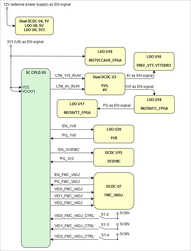
Power-On Sequence
The TEF1001 board meets the recommended criteria to power up the Xilinx FPGA properly by keeping a specific sequence of enabling the on-board DC-DC converters dedicated to the particular functional units of the FPGA chip and powering up the on-board voltages.
Some of the voltages are handled by the System Controller CPLD using "Power good"-signals from the voltage regulators:
Following diagram clarifies the sequence of enabling the particular on-board voltages, which will power-up in descending order as listed in the blocks of the diagram:
| Scroll Title | ||||||||||||||||||||||||||||||||
|---|---|---|---|---|---|---|---|---|---|---|---|---|---|---|---|---|---|---|---|---|---|---|---|---|---|---|---|---|---|---|---|---|
| ||||||||||||||||||||||||||||||||
|
Power Rails
| Bank | Schematic Name | Voltage | Range | Notes |
|---|---|---|---|---|
| 0 | 1V8 | 1.8V | HP: 1.2V to 1.8V | Config bank (fixed to 1.8V) / JTAG interface. |
| 14 | 1V8 | 1.8V | HP: 1.2V to 1.8V | QSPI flash memory interface. |
| 15 | 1V8 | 1.8V | HP: 1.2V to 1.8V | Reference clock input. |
| 16 | 1V8 | 1.8V | HP: 1.2V to 1.8V | I2C interface of FPGA. |
| 17 | 1V8 | 1.8V | HP: 1.2V to 1.8V | Reference clock input. |
| 18 | 1V8 | 1.8V | HP: 1.2V to 1.8V | Reference clock input / I/O's to CPLD. |
| 34 | VCC1V5 | 1.5V | HP: 1.2V to 1.8V | DDR3 memory interface. |
| 35 | VCC1V5 | 1.5V | HP: 1.2V to 1.8V | DDR3 memory interface. |
| 36 | VCC1V5 | 1.5V | HP: 1.2V to 1.8V | DDR3 memory interface. |
114 115 116 117 118 | MGTAVCC_FPGA MGTVCCAUX_FPGA MGTAVTT_FPGA | 1.0V 1.8V 1.2V | MGT bank supply voltage MGT bank auxiliary supply voltage MGT bank termination circuits voltage | MGT banks with Xilinx GTH transceiver units. |
| 19 | 1V8 | 1.8V | HP: 1.2V to 1.8V | I/Os routed to FMC, usable as LVDS pairs. |
| 37 | 1V8 | 1.8V | HP: 1.2V to 1.8V | I/Os routed to FMC, usable as LVDS pairs. |
| 38 | 1V8 | 1.8V | HP: 1.2V to 1.8V | I/Os routed to FMC, usable as LVDS pairs. |
| 39 | VIO_B_FMC | user | HP: 1.2V to 1.8V | I/Os routed to FMC, usable as LVDS pairs. |
Table 15: Module power rails
Bank Voltages
| Connector / Pin | Voltage | Direction | Notes |
|---|---|---|---|
| J4, pin 2 | 12V (filtered) | Output | 4-wire PWM fan connector supply voltage |
| J6, pin 2 | 5V (filtered) | Output | Cooling fan M1 supply voltage |
| J8, pin 6 | 3V3PCI | Output | VCCIO CPLD JTAG |
| J9, pin 2 | 1V8 | Output | VCCIO FPGA JTAG |
| J2, pin C35 / C37 | 12V | Output | VCCIO FMC |
| J2, pin D32 | 3V3PCI | Output | VCCIO FMC |
| J2, pin D36 / D38 / D39 / D40 | 3V3FMC | Output | VCCIO FMC |
| J2, pin H1 | VREF_A_M2C | Input | VREF voltage for bank 37 / 38 |
| J2, pin K1 | VREF_B_M2C | Input | VREF voltage for bank 39 |
| J2, pin J39 / J40 | VIO_B_FMC | Input | PL I/O voltage bank 39 (VCCO) |
| J2, pin H40 / G39 / F40 / E39 | FMC_VADJ | Output | VCCIO FMC (fixed to 1.8V) |
| J1, pin A10 / A11 / B8 | 3V3PCI | Input | PCIe interface supply voltage |
| J5, pin 1 / 2 / 3 | 12V | Input | Main power supply connector |
Table 16Table 14: Module PL I/O bank voltages
...
Parameter | Min | Max | Units | Reference Document |
|---|---|---|---|---|
VIN supply voltage | -0.3 | 20 | V | TPS6217 datasheet Caution with FMC module plugged in and/or FPGA FAN connected: |
| Supply voltage for HR I/O banks (VCCO) | -0.500 | 3.600 | V | Xilinx datasheet DS182 |
Supply voltage for HP I/O banks (VCCO) | -0.500 | 2.000 | V | Xilinx datasheet DS182 |
| I/O input voltage for HR I/O banks | -0.500 | VCCO + 0.500 | V | Xilinx datasheet DS182 |
I/O input voltage for HP I/O banks | -0.500 | VCCO + 0.500 | V | Xilinx datasheet DS182 |
| Reference Voltage pin (VREF) | -0.500 | 2 | V | Xilinx datasheet DS182 |
| Differential input voltage | -0.5 | 2.625 | V | Xilinx datasheet DS182 |
| I/O input voltage for SC CPLD U5 | -0.5 | 3.75 | V | Lattice MachXO2 Family datasheet |
| GTH and GTY transceiver reference clocks absolute input voltage (MGT_CLK0, MGT_CLK2) | -0.500 | 1.320 | V | Xilinx datasheet DS182 |
GTH and GTY transceiver receiver (RXP/RXN) and transmitter (TXP/TXN) absolute input voltage | -0.500 | 1.260 | V | Xilinx datasheet DS182 |
| Voltages on LTM4676 I²C pins (LTM_SCL, LTM_SDA), header J10 | -0.3 | 5.5 | V | LTM4676A datasheet |
Storage temperature | -40 | +100 | °C | SML-P11 LED datasheet |
Table 1617: Module absolute maximum ratings
...
| Parameter | Min | Max | Units | Reference Document |
|---|---|---|---|---|
| VIN supply voltage | 11.4 | 12.6 | V | 12V nominal, ANSI/VITA 57.1 power specification for FMC connector |
| Supply voltage for HR I/O banks (VCCO) | 1.140 | 3.465 | V | Xilinx datasheet DS182 |
Supply voltage for HP I/O banks (VCCO) | 1.140 | 1.890 | V | Xilinx datasheet DS182 |
I/O input voltage for HR I/O banks | –0.500 | VCCO + 0.20 | V | Xilinx datasheet DS182 |
| I/O input voltage for HP I/O banks | –0.500 | VCCO + 0.20 | V | Xilinx datasheet DS182 |
| Differential input voltage | -0.2 | 2.625 | V | Xilinx datasheet DS182 |
| I/O input voltage for SC CPLD U5 | -0.3 | 3.6 | V | Lattice MachXO2 Family datasheet |
| Voltages on LTM4676 I²C pins (LTM_SCL, LTM_SDA), header J10 | 0 | 3.3V | V | LTM4676A datasheet |
Industrial Module Operating Temperature Range | -40 | 85 | °C | Xilinx datasheet DS182 |
| Commercial Module Operating Temperature Range | 0 | 85 | °C | Xilinx DS182, Silicon Labs Si5338 datasheets |
Table 1718: Module recommended operating conditions
...
Board size: 50 mm × 40 mm. Please download the assembly diagram for exact numbers.
PCB thickness: ca. 1.55 mm.
The board meets the PCIe standard specifications for the dimensions of a PCIe card
All dimensions are given in millimeters.
...
| Date | Revision | Notes | PCN | Documentation Link |
|---|---|---|---|---|
| - | 02 | current available board revision | - | - |
| - | 01 | First production release | PCN-20180524 TEF1001-01 | TEF1001-01 |
Table 1819: Module hardware revision history
...
Date | Revision | Contributors | Description | ||||||||||||||||||||||||||
|---|---|---|---|---|---|---|---|---|---|---|---|---|---|---|---|---|---|---|---|---|---|---|---|---|---|---|---|---|---|
|
|
|
|
Table 1820: Document change history
Disclaimer
...
Overview
Content Tools